JP2004264332A - Multiple image forming position shift detecting device, image density detecting device, and multiple image forming device - Google Patents
Multiple image forming position shift detecting device, image density detecting device, and multiple image forming device Download PDFInfo
- Publication number
- JP2004264332A JP2004264332A JP2003016559A JP2003016559A JP2004264332A JP 2004264332 A JP2004264332 A JP 2004264332A JP 2003016559 A JP2003016559 A JP 2003016559A JP 2003016559 A JP2003016559 A JP 2003016559A JP 2004264332 A JP2004264332 A JP 2004264332A
- Authority
- JP
- Japan
- Prior art keywords
- light
- image
- image forming
- output
- photosensitive
- Prior art date
- Legal status (The legal status is an assumption and is not a legal conclusion. Google has not performed a legal analysis and makes no representation as to the accuracy of the status listed.)
- Pending
Links
Images






Classifications
-
- G—PHYSICS
- G03—PHOTOGRAPHY; CINEMATOGRAPHY; ANALOGOUS TECHNIQUES USING WAVES OTHER THAN OPTICAL WAVES; ELECTROGRAPHY; HOLOGRAPHY
- G03G—ELECTROGRAPHY; ELECTROPHOTOGRAPHY; MAGNETOGRAPHY
- G03G15/00—Apparatus for electrographic processes using a charge pattern
-
- H—ELECTRICITY
- H04—ELECTRIC COMMUNICATION TECHNIQUE
- H04N—PICTORIAL COMMUNICATION, e.g. TELEVISION
- H04N1/00—Scanning, transmission or reproduction of documents or the like, e.g. facsimile transmission; Details thereof
- H04N1/46—Colour picture communication systems
- H04N1/50—Picture reproducers
- H04N1/506—Reproducing the colour component signals picture-sequentially, e.g. with reproducing heads spaced apart from one another in the subscanning direction
-
- G—PHYSICS
- G03—PHOTOGRAPHY; CINEMATOGRAPHY; ANALOGOUS TECHNIQUES USING WAVES OTHER THAN OPTICAL WAVES; ELECTROGRAPHY; HOLOGRAPHY
- G03G—ELECTROGRAPHY; ELECTROPHOTOGRAPHY; MAGNETOGRAPHY
- G03G15/00—Apparatus for electrographic processes using a charge pattern
- G03G15/01—Apparatus for electrographic processes using a charge pattern for producing multicoloured copies
-
- G—PHYSICS
- G03—PHOTOGRAPHY; CINEMATOGRAPHY; ANALOGOUS TECHNIQUES USING WAVES OTHER THAN OPTICAL WAVES; ELECTROGRAPHY; HOLOGRAPHY
- G03G—ELECTROGRAPHY; ELECTROPHOTOGRAPHY; MAGNETOGRAPHY
- G03G15/00—Apparatus for electrographic processes using a charge pattern
- G03G15/01—Apparatus for electrographic processes using a charge pattern for producing multicoloured copies
- G03G15/0142—Structure of complete machines
- G03G15/0178—Structure of complete machines using more than one reusable electrographic recording member, e.g. one for every monocolour image
- G03G15/0194—Structure of complete machines using more than one reusable electrographic recording member, e.g. one for every monocolour image primary transfer to the final recording medium
-
- H—ELECTRICITY
- H10—SEMICONDUCTOR DEVICES; ELECTRIC SOLID-STATE DEVICES NOT OTHERWISE PROVIDED FOR
- H10F—INORGANIC SEMICONDUCTOR DEVICES SENSITIVE TO INFRARED RADIATION, LIGHT, ELECTROMAGNETIC RADIATION OF SHORTER WAVELENGTH OR CORPUSCULAR RADIATION
- H10F39/00—Integrated devices, or assemblies of multiple devices, comprising at least one element covered by group H10F30/00, e.g. radiation detectors comprising photodiode arrays
- H10F39/10—Integrated devices
- H10F39/12—Image sensors
-
- H—ELECTRICITY
- H10—SEMICONDUCTOR DEVICES; ELECTRIC SOLID-STATE DEVICES NOT OTHERWISE PROVIDED FOR
- H10F—INORGANIC SEMICONDUCTOR DEVICES SENSITIVE TO INFRARED RADIATION, LIGHT, ELECTROMAGNETIC RADIATION OF SHORTER WAVELENGTH OR CORPUSCULAR RADIATION
- H10F39/00—Integrated devices, or assemblies of multiple devices, comprising at least one element covered by group H10F30/00, e.g. radiation detectors comprising photodiode arrays
- H10F39/80—Constructional details of image sensors
- H10F39/802—Geometry or disposition of elements in pixels, e.g. address-lines or gate electrodes
-
- G—PHYSICS
- G03—PHOTOGRAPHY; CINEMATOGRAPHY; ANALOGOUS TECHNIQUES USING WAVES OTHER THAN OPTICAL WAVES; ELECTROGRAPHY; HOLOGRAPHY
- G03G—ELECTROGRAPHY; ELECTROPHOTOGRAPHY; MAGNETOGRAPHY
- G03G2215/00—Apparatus for electrophotographic processes
- G03G2215/01—Apparatus for electrophotographic processes for producing multicoloured copies
- G03G2215/0103—Plural electrographic recording members
- G03G2215/0119—Linear arrangement adjacent plural transfer points
-
- G—PHYSICS
- G03—PHOTOGRAPHY; CINEMATOGRAPHY; ANALOGOUS TECHNIQUES USING WAVES OTHER THAN OPTICAL WAVES; ELECTROGRAPHY; HOLOGRAPHY
- G03G—ELECTROGRAPHY; ELECTROPHOTOGRAPHY; MAGNETOGRAPHY
- G03G2215/00—Apparatus for electrophotographic processes
- G03G2215/01—Apparatus for electrophotographic processes for producing multicoloured copies
- G03G2215/0151—Apparatus for electrophotographic processes for producing multicoloured copies characterised by the technical problem
- G03G2215/0158—Colour registration
- G03G2215/0161—Generation of registration marks
Landscapes
- Physics & Mathematics (AREA)
- General Physics & Mathematics (AREA)
- Engineering & Computer Science (AREA)
- Multimedia (AREA)
- Signal Processing (AREA)
- Color Electrophotography (AREA)
- Control Or Security For Electrophotography (AREA)
- Image Processing (AREA)
- Length Measuring Devices By Optical Means (AREA)
- Facsimile Heads (AREA)
- Solid State Image Pick-Up Elements (AREA)
Abstract
【課題】多重画像形成位置ずれ検出用パターン検出処理の高速化および構成の簡素化を図ることができる多重画像形成位置ずれ検出装置を提供すること。
【解決手段】光検出部5は、光感応領域10と、第1信号処理回路20と、第2信号処理回路30とを有する。光感応領域10は、画素11mnがM行N列に2次元配列されている。1画素は、各々に入射した光の強度に応じた電流を出力する光感応部分12mn及び光感応部分13mnを同一面内にて隣接して配設することで構成される。2次元配列における第1の方向に配列された複数の画素1111〜111N,・・・,11M1〜11MNにわたって、一方の光感応部分12mn同士が互いに電気的に接続されている。また、2次元配列における第2の方向に配列された複数の画素1111〜11M1,・・・,111N〜11MNにわたって、他方の光感応部分13mn同士が互いに電気的に接続されている。
【選択図】 図5A multiplex image forming position shift detecting device capable of speeding up a multiplex image forming position shift detecting pattern detection process and simplifying the configuration.
A light detection unit includes a light sensitive area, a first signal processing circuit, and a second signal processing circuit. In the photosensitive region 10, pixels 11 mn are two-dimensionally arranged in M rows and N columns. One pixel is configured by arranging a light-sensitive portion 12 mn and a light-sensitive portion 13 mn that output a current corresponding to the intensity of light incident on each pixel adjacently in the same plane. One of the light-sensitive portions 12 mn is electrically connected to each other over the plurality of pixels 11 11 to 11 1N ,..., 11 M1 to 11 MN arranged in the first direction in the two-dimensional array. Further, a plurality of pixels 11 11 to 11 M1 arranged in the second direction in the two-dimensional array, ..., 11 over 1N to 11 MN, and the other photosensitive portions 13 mn each other are electrically connected to each other I have.
[Selection diagram] FIG.
Description
【0001】
【発明の属する技術分野】
本発明は、多重画像形成位置ずれ検出装置、画像濃度検出装置及び多重画像形成装置に関する。
【0002】
【従来の技術】
この種の多重画像形成装置として、多重画像を形成するために複数個の画像形成部が配置され、各画像形成部にてそれぞれ色の異なった各画像を形成し、転写材に転写され重ねられる該各画像の転写位置のずれを補正するための多重画像形成位置ずれ検出用パターン(位置決めパターン)をCCDイメージセンサにて読み取るものが知られている(例えば、特許文献1参照。)。また、特許文献1においては、転写材上に転写される画像の濃度を制御するための濃度検出用パターンもCCDイメージセンサにて読み取っている。
【0003】
【特許文献1】
特開平1−167769号公報
【0004】
【発明が解決しようとする課題】
しかしながら、多重画像形成位置ずれ検出用パターンあるいは濃度検出用パターンの読み取りにCCDイメージセンサを用いていたのでは、以下のような問題点を有することとなる。CCDイメージセンサにおいては、1フレーム内の光強度分布を得るには、全ての画素についてデータ処理(例えば、m×n画素を有する場合、m×n回のデータ処理)が必要となり、データ処理の時間が長くなってしまう。また、データ処理を行う信号処理回路として、高性能化、高速化のものが要求されてしまう。
【0005】
本発明は上述の点に鑑みてなされたもので、多重画像形成位置ずれ検出用パターンの検出処理の高速化および構成の簡素化を図ることができる多重画像形成位置ずれ検出装置、同じく濃度検出用パターンの検出処理の高速化および構成の簡素化を図ることができる画像濃度検出装置、同じく多重画像形成位置ずれ検出用パターンあるいは濃度検出用パターンの検出処理の高速化および構成の簡素化を図ることができる多重画像形成装置を提供することを課題とする。
【0006】
【課題を解決するための手段】
本発明に係る多重画像形成位置ずれ検出装置は、多重画像を形成する際に各画像の転写位置のずれを検出するために、被検出対象の表面に形成された多重画像形成位置ずれ検出用パターンを、画素が2次元配列された光感応領域を有する光検出手段によって検出する多重画像形成位置ずれ検出装置であって、光検出手段は、各々入射した光の強度に応じた電流を出力する複数の光感応部分を同一面内にて隣接して配設することで1画素が構成されており、2次元配列における第1の方向に配列された複数の画素にわたって、当該各画素を構成する複数の光感応部分のうち一方の光感応部分同士が電気的に接続され、2次元配列における第2の方向に配列された複数の画素にわたって、当該各画素を構成する複数の光感応部分のうち他方の光感応部分同士が電気的に接続されていることを特徴としている。
【0007】
本発明に係る多重画像形成位置ずれ検出装置では、光検出手段において、1つの画素に入射した光は当該画素を構成する複数の光感応部分それぞれにおいて検出されて、光強度に応じた電流が光感応部分毎に出力される。そして、一方の光感応部分同士が2次元配列における第1の方向に配列された複数の画素にわたって電気的に接続されているので、一方の光感応部分からの電流出力は第1の方向に送られる。また、他方の光感応部分同士が2次元配列における第2の方向に配列された複数の画素にわたって電気的に接続されているので、他方の光感応部分からの電流出力は第2の方向に送られる。このように、一方の光感応部分からの電流出力は第1の方向に送られるとともに、他方の光感応部分からの電流出力は第2の方向に送られることから、第1の方向での輝度プロファイルと第2の方向での輝度プロファイルとをそれぞれ独立して得ることが可能となる。この結果、1画素に複数の光感応部分を配設するという極めて簡素な構成にて、多重画像形成位置ずれ検出用パターンの第1の方向での輝度プロファイル及び第2の方向での輝度プロファイルを高速に検出することができる。
【0008】
本発明に係る画像濃度検出装置は、画像の濃度を検出するために、被検出対象の表面に形成された濃度検出用パターンを、画素が2次元配列された光感応領域を有する光検出手段によって検出する画像濃度検出装置であって、光検出手段は、各々入射した光の強度に応じた電流を出力する複数の光感応部分を同一面内にて隣接して配設することで1画素が構成されており、2次元配列における第1の方向に配列された複数の画素にわたって、当該各画素を構成する複数の光感応部分のうち一方の光感応部分同士が電気的に接続され、2次元配列における第2の方向に配列された複数の画素にわたって、当該各画素を構成する複数の光感応部分のうち他方の光感応部分同士が電気的に接続されていることを特徴としている。
【0009】
本発明に係る画像濃度検出装置では、光検出手段において、1つの画素に入射した光は当該画素を構成する複数の光感応部分それぞれにおいて検出されて、光強度に応じた電流が光感応部分毎に出力される。そして、一方の光感応部分同士が2次元配列における第1の方向に配列された複数の画素にわたって電気的に接続されているので、一方の光感応部分からの電流出力は第1の方向に送られる。また、他方の光感応部分同士が2次元配列における第2の方向に配列された複数の画素にわたって電気的に接続されているので、他方の光感応部分からの電流出力は第2の方向に送られる。このように、一方の光感応部分からの電流出力は第1の方向に送られるとともに、他方の光感応部分からの電流出力は第2の方向に送られることから、第1の方向での輝度プロファイルと第2の方向での輝度プロファイルとをそれぞれ独立して得ることが可能となる。この結果、1画素に複数の光感応部分を配設するという極めて簡素な構成にて、濃度検出用パターンの第1の方向での輝度プロファイル及び第2の方向での輝度プロファイルを高速に検出することができる。
【0010】
また、上記光検出手段は、第1の方向に配列された複数の画素間において電気的に接続された一方の光感応部分群からの出力を読み出して当該出力に基づいて2次元配列における第2の方向での輝度プロファイルを検出する第1信号処理回路と、第2の方向に配列された複数の画素間において電気的に接続された他方の光感応部分群からの出力を読み出して当該出力に基づいて2次元配列における第1の方向での輝度プロファイルを検出する第2信号処理回路と、を有することが好ましい。
【0011】
本発明に係る多重画像形成装置は、多重画像を形成するために、それぞれ異なった各画像を形成する複数個の画像形成部と、上記多重画像形成位置ずれ検出装置と、を備え、画像形成部によりそれぞれ形成された各画像の転写位置のずれを多重画像形成位置ずれ検出装置により検出することを特徴としている。
【0012】
本発明に係る多重画像形成装置では、上記多重画像形成位置ずれ検出装置を備えているので、1画素に複数の光感応部分を配設するという極めて簡素な構成にて、多重画像形成位置ずれ検出用パターンの第1の方向での輝度プロファイル及び第2の方向での輝度プロファイルを高速に検出することができる。
【0013】
本発明に係る多重画像形成装置は、多重画像を形成するために、それぞれ異なった各画像を形成する複数個の画像形成部と、上記画像濃度検出装置と、を備え、画像形成部によりそれぞれ形成された各画像の濃度を画像濃度検出装置により検出することを特徴としている。
【0014】
本発明に係る多重画像形成装置では、上記画像濃度検出装置を備えているので、1画素に複数の光感応部分を配設するという極めて簡素な構成にて、濃度検出用パターンの第1の方向での輝度プロファイル及び第2の方向での輝度プロファイルを高速に検出することができる。
【0015】
【発明の実施の形態】
本発明に係る実施形態について図面を参照して説明する。なお、説明において、同一要素又は同一機能を有する要素には、同一符号を用いることとし、重複する説明は省略する。以下では、パラメータMおよびNそれぞれを2以上の整数とする。また、特に明示しない限りは、パラメータmを1以上M以下の任意の整数とし、パラメータnを1以上N以下の任意の整数とする。
【0016】
図1は、本実施形態に係る多重画像形成装置を示す概略構成図であり、たとえば、4ドラム方式のカラーレーザビームプリンタの場合に対応する。なお、本実施形態に係る多重画像形成装置は、本発明の実施形態に係る多重画像形成位置ずれ検出装置及び画像濃度検出装置を含んでいる。
【0017】
カラーレーザビームプリンタ101(多重画像形成装置)は、イエロー用画像形成ステーション102Y、マゼンタ用画像形成ステーション102M、シアン用画像形成ステーション102C及びブラック用画像形成ステーション102Kを備えている。
【0018】
イエロー用画像形成ステーション102Yは、クリーナ103Y、帯電器104Y、現像ユニット105Y及び像担持体としての感光ドラム106Yが設けられている。感光ドラム106Yに対しては、潜像を形成するためのイエロー用露光ユニット107Yが設けられている。イエロー用露光ユニット107Yは、レーザ走査手段108Yを有し、画像信号に基づいてパルス幅変調された走査ビーム109Yを感光ドラム106Yに対して発射する。転写ベルト110は、ドライブモータ(図示せず)により回転駆動される駆動ローラ112と従動ローラ113とに掛け渡されており、駆動ローラ112が回転することにより移動する。転写ベルト110を挟んで感光ドラム106Yと対向する位置に、イエロー用転写ユニット114Yが設けられている。イエロー用転写ユニット114Yは、転写ベルト110表面上に、イエロー用画像形成ステーション102Yの感光ドラム106Y上に現像されたイエロー色画像記録材による画像を転写する。ここで、イエロー用画像形成ステーション102Y、イエロー用露光ユニット107Y及びイエロー用転写ユニット114Yが、イエロー用画像形成部を構成している。
【0019】
マゼンタ用画像形成ステーション102Mは、クリーナ103M、帯電器104M、現像ユニット105M及び像担持体としての感光ドラム106Mが設けられている。感光ドラム106Mに対しては、潜像を形成するためのマゼンタ用露光ユニット107Mが設けられている。マゼンタ用露光ユニット107Mは、レーザ走査手段108Mを有し、画像信号に基づいてパルス幅変調された走査ビーム109Mを感光ドラム106Mに対して発射する。転写ベルト110を挟んで感光ドラム106Mと対向する位置に、マゼンタ用転写ユニット114Mが設けられている。マゼンタ用転写ユニット114Mは、転写ベルト110表面上に、マゼンタ用画像形成ステーション102Mの感光ドラム106M上に現像されたマゼンタ色画像記録材による画像を転写する。ここで、マゼンタ用画像形成ステーション102M、マゼンタ用露光ユニット107M及びマゼンダ用転写ユニット114Mが、マゼンタ用画像形成部を構成している。
【0020】
シアン用画像形成ステーション102Cは、クリーナ103C、帯電器104C、現像ユニット105C及び像担持体としての感光ドラム106Cが設けられている。感光ドラム106Cに対しては、潜像を形成するためのシアン用露光ユニット107Cが設けられている。シアン用露光ユニット107Cは、レーザ走査手段108Cを有し、画像信号に基づいてパルス幅変調された走査ビーム109Cを感光ドラム106Cに対して発射する。転写ベルト110を挟んで感光ドラム106Cと対向する位置に、シアン用転写ユニット114Cが設けられている。シアン用転写ユニット114Cは、転写ベルト110表面上に、シアン用画像形成ステーション102Cの感光ドラム106C上に現像されたシアン色画像記録材による画像を転写する。ここで、シアン用画像形成ステーション102C、シアン用露光ユニット107C及びシアン用転写ユニット114Cが、シアン用画像形成部を構成している。
【0021】
ブラック用画像形成ステーション102Kは、クリーナ103K、帯電器104K、現像ユニット105K及び像担持体としての感光ドラム106Kが設けられている。感光ドラム106Kに対しては、潜像を形成するためのブラック用露光ユニット107Kが設けられている。ブラック用露光ユニット107Kは、レーザ走査手段108Kを有し、画像信号に基づいてパルス幅変調された走査ビーム109Kを感光ドラム106Kに対して発射する。転写ベルト110を挟んで感光ドラム106Kと対向する位置に、ブラック用転写ユニット114Kが設けられている。ブラック用転写ユニット114Kは、転写ベルト110表面上に、ブラック用画像形成ステーション102Kの感光ドラム106K上に現像されたブラック色画像記録材による画像を転写する。ここで、ブラック用画像形成ステーション102K、ブラック用露光ユニット107K及びブラック用転写ユニット114Kが、ブラック用画像形成部を構成している。
【0022】
各色画像形成ステーション102Y,102M,102C,102Kの下方に位置する転写ベルト110の搬送経路上には、転写紙用転写ユニット115が設けられている。転写紙用転写ユニット115は、転写ベルト110を挟んで一組の転写ローラ115a,115bを有しており、転写ベルト110表面上に転写された各色画像を転写紙に転写する。
【0023】
用紙としての転写紙Paは、複数のカセット116a,116b,116cに収納され、バネ(図示せず)により上面側の転写紙Paが各ピックアップローラ117a,117b,117cに当接するように底上げされている。各ピックアップローラ117a,117b,117cにより分離された転写紙Paは、搬送路118上を転写紙用転写ユニット115の配設方向に搬送される。搬送路118には、搬送ローラ118aが所定間隔を置いて設けられている。転写紙用転写ユニット115により各色画像が転写された転写紙Paは、搬送ベルト119により定着ユニット120に搬送される。定着ユニット120は、熱定着ローラ120aと加圧ローラ120bとを有しており、転写紙Paに転写された各色画像(トナー像)を熱溶融定着させる。
【0024】
定着ユニット120により各色画像が定着された転写紙Paは、排出搬送路121を通ってカラーレーザビームプリンタ101外部に排出される。排出搬送路121の途中部分からは、裏面プリントのために転写紙を反転する転写紙反転搬送路122が分岐して設けられている。転写紙反転搬送路122からは、搬送路123が分岐しており、搬送路123は搬送路118の途中部分に接続されるよう構成されている。搬送路123には、搬送ローラ123aが所定間隔を置いて設けられている。
【0025】
このように各色画像形成ステーション102Y,102M,102C,102Kを有するカラーレーザビームプリンタ101において、画像を形成する際には、イエロー(Y)、マゼンタ(M)、シアン(C)、ブラック(K)の各色に対応する各色画像形成部分の両端部に、多重画像形成位置ずれ検出用パターンとしての位置決めマーク像7を、カールソンプロセス等の所定のプロセスを介し、それぞれ、イエロー、マゼンタ、シアン、ブラックの各色に対して形成し(図3に示されているように、各色に対し形成された位置決めマーク像をそれぞれ7Y,7M,7C,7Kとする)、順次転写ベルト110上に転写する。
【0026】
転写ベルト110上において、各色画像形成部分の両端部に形成されるこの位置決めマーク像7は、図3に示されているように、転写ベルト110の搬送方向と直交する方向、すなわち主走査方向の各画像形成部の右側端及び左側端に転写され、しかもその転写位置は、転写ベルト110の搬送方向、すなわち副走査方向(図中、矢印A方向)に対してイエロー、マゼンタ、シアン、ブラックの順にそれぞれが混色しないようにずらしてある。
【0027】
転写ベルト110上において各画像形成部分の右側端及び左側端に転写された位置決めマーク像7は、図2に示されるように、これを検出するように、それぞれに対応して配設された、多重画像形成位置ずれ検出装置1により検出される。この多重画像形成位置ずれ検出装置1は、発光素子を有する発光部3と、位置決めマーク像検出部としての光検出部(光検出手段)5とを含んでいる。
【0028】
位置決めマーク像7の検出は、位置決めマーク像7が、転写ベルト110と共に搬送され、図3に示されるように、光検出部5の位置決めマーク像検出領域5aに達すると、位置決めマーク像検出手段(図示せず)の作動により転写ベルト110のやや上方に配設された発光部3(発光素子)を作動させ、この発光部3(発光素子)からの光を、転写ベルト110上の位置決めマーク像7で反射させ、この反射光を光検出部5で検出することにより行なわれる。
【0029】
その際、位置決めマーク像7の検出は赤外域(750〜950nm)で行なわれることが望ましくその理由は、4色(イエロー、マゼンタ、シアン、ブラック)の各トナーで転写ベルト110上に書かれた各位置決めマーク像をできるだけ同感度で検出するためである。また、転写ベルト110は透明であるため、位置決めマーク像7以外からの光の入射は殆どない。
【0030】
このようにして、光検出部5で検出された反射光は、CPU(中央処理装置)に入力されて処理され、このCPU(中央処理装置)により位置決めマーク像7の位置が求められて、レジストレーションのずれ量が演算される。このとき、位置決めマーク像7の転写位置は、既知であり、CPU(中央処理装置)でレジストレーションが正確に合っていると判断された場合は、CPU(中央処理装置)の指示により、この既知の位置に転写される。逆に、CPU(中央処理装置)でレジストレーションが悪化していると判断された場合には、この既知の値と位置決めマーク像7が実際に転写された位置との誤差をCPU(中央処理装置)で演算することによりずれ量を求める。
【0031】
このずれ量に応じて、上記レーザ走査手段108Y,108M,108C,108Kレーザ光路中にある反射ミラーをステッピングモータ(図示せず)を用いて作動させ、倍率、副走査方向の傾き、平行移動等を調整することにより、レジストレーションを合わせる。なお、レジストレーションのずれ量を、上記した他に感光ドラムや転写ベルトの駆動を制御して補正することもできる。また、レジストレーションのずれ量を、上記した他に転写紙用転写ユニット115付近で転写ベルト110と転写紙用転写ユニット115との相対位置を主走査方向に移動することで補正することもできる。
【0032】
このレジストレーション補正は、上記各色画像形成ステーション102Y,102M,102C,102Kのうちの1つを基準の画像形成ステーションとし、その際、基準画像形成ステーションの補正は、いっさい行わず、他の3つの画像形成ステーションをこの基準画像形成ステーションに合わせるようにして行なわれる。
【0033】
ここで、位置決めマーク像7は、一度に2方向のずれを検出することができるものとされる。本実施形態において、位置決めマーク像7は、図3に示されるように、「+」形状(十字形状)を呈している。位置決めマーク像7は、これ以外に、「◎」形状、「T」形状、「◇」形状、「●」形状等であってもよい。そして所望の色の画像形成に必要とされ、読み取られた転写ベルト上の位置決めマーク像はベルト用クリーナブレード(図示せず)の作動により転写ベルト110上から除去され、次の画像形成が可能となる。
【0034】
次に、図4を参照して、転写ベルト110上に形成される濃度検出用パターンの読み取り(検出)について説明する。
【0035】
まず、この濃度検出用パターンの検出は、レジストレーション補正の際の位置決めマーク像の検出とは別に行なわれる。図4に示すように、濃度検出用パターン9のプリントについては、階調を変えた一様な濃度パッチを有する濃度検出用パターン9が、各色ごとに、前述した多重画像形成位置ずれ検出装置1、すなわち位置決めマーク像検出部と共用される濃度検出用パターン検出部としての光検出部5の検出領域5aもしくはそれよりも広い領域の範囲で、カールソンプロセス等の所定のプロセスを介して形成される数階調の濃度パッチを、ある間隔をもって転写ベルト110の右、左の両端あるいは両端のどちらか一方に、光検出部5に対応するように、転写ベルト110上の位置にプリントする。したがって、多重画像形成位置ずれ検出装置1が、画像の濃度を検出するため画像濃度検出装置として機能することとなる。
【0036】
数階調の濃度パッチを有する濃度検出用パターン9の転写ベルト110への転写は、転写ベルト110上に1色ずつ適当な間隔をもって行なわれ、それぞれ、イエロー、マゼンタ、シアン、ブラックの各色について行なわれる。この濃度検出用パターン9は、各色ごとに転写ベルト110の左右両端どちらか、もしくはその両端に転写される。転写ベルト110上に形成された濃度検出用パターン9は、光検出部5で濃度検出用パターン9の濃度パッチを検出した後は、ベルトクリーナ(図示せず)でクリーニングされる。
【0037】
光検出部5で検出された濃度検出用パターンの出力値は、あらかじめ測定された光検出部5の出力と画像濃度との関係に基づいて画像濃度に変換され、これにより、その時の画像の階調性を知ることができ、濃度制御が行なわれる。また、その際、感光ドラム上の濃度検出用パターンにおける濃度パッチに対応する位置の表面電位を同時に測定することで、画像の濃度特性にとって重要であるV−D特性を把握でき、画像濃度を制御する際の基礎データとすることができ、このV−D特性から適正なコントラスト電位を求め、レーザパワー、グリッドバイアス、現像バイアス等を変えることで、画像の濃度制御が行なわれる。
【0038】
以上、述べてきたレジストレーション補正及び画像の濃度制御は、別々の動作であり、それぞれの動作が行なわれるタイミングは、レジストレーション補正に関しては各色のレジストレーションのずれ量が常にあらかじめ定められた範囲内に収まるように、また、画像の濃度制御に関しては、各色の画像の濃度もしくは階調性が一定に保たれるように行なわれる。このように、レジストレーション補正により転写ずれのない状態で、なおかつ画像の濃度制御により各色の画像の濃度及び階調性が適正に保たれている状態において、プリント動作が行なわれる。
【0039】
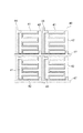
次に、図5〜図17を参照して、上記光検出部5について詳細に説明する。図5は、本実施形態に係る光検出装置を示す概念構成図である。光検出部5は、図5に示されるように、光感応領域10と、第1信号処理回路20と、第2信号処理回路30とを有している。
【0040】
光感応領域10は、画素11mnがM行N列に2次元配列されている。1画素は、各々に入射した光の強度に応じた電流を出力する光感応部分12mn(第1光感応部分)及び光感応部分13mn(第2光感応部分)を同一面内にて隣接して配設することで構成されている。これにより、光感応領域10において、光感応部分12mnと光感応部分13mnとは2次元的に混在した状態で同一面内にて配列されることとなる。
【0041】
2次元配列における第1の方向に配列された複数の画素1111〜111N,1121〜112N,・・・,11M1〜11MNにわたって、当該各画素11mnを構成する複数の光感応部分12mn,13mnのうち一方の光感応部分12mn同士(たとえば、一方の光感応部分1211〜121N)が互いに電気的に接続されている。また、2次元配列における第2の方向に配列された複数の画素1111〜11M1,1112〜11M2,・・・,111N〜11MNにわたって、当該各画素11mnを構成する複数の光感応部分12mn,13mnのうち他方の光感応部分13mn同士(たとえば、他方の光感応部分1311〜13M1)が互いに電気的に接続されている。
【0042】
ここで、図6及び図7に基づいて、光感応領域10の構成について説明する。図6は、光感応領域の一例を示す要部拡大平面図であり、図7は、図6のVII−VII線に沿った断面図である。なお、図6においては、保護層48の図示を省略している。
【0043】
光感応領域10は、P型(第1導電型)の半導体からなる半導体基板40と、当該半導体基板40の表層に形成されたN型(第2導電型)の半導体領域41,42とを含んでいる。これにより、各光感応部分12mn,13mnは半導体基板40部分と一組の第2導電型半導体領域41,42とを含み、フォトダイオードが構成されることとなる。第2導電型半導体領域41,42は、図6に示されるように、光入射方向から見て略三角形状を呈しており、1画素において2つの領域41,42が互いに一辺が隣接して形成されている。半導体基板40は、接地電位とされている。なお、光感応領域10は、N型の半導体からなる半導体基板と、当該半導体基板の表層に形成されたP型の半導体領域とを含んで構成されていてもよい。領域41(光感応部分12mn)と領域42(光感応部分13mn)とは、図6から分かるように、第1の方向及び第2の方向において交互に配列されている。また、領域41(光感応部分12mn)と領域42(光感応部分13mn)とは、第1の方向と第2の方向とに交差する(たとえば、45°にて交差する)第3の方向及び第4の方向において交互に配列されている。
【0044】
半導体基板40と領域41,42の上には第1絶縁層43が形成され、この第1絶縁層43に形成されたコンタクトホールを介して第1配線44が一方の領域41に電気的に接続されている。また、第1絶縁層43に形成されたコンタクトホールを介して電極45が他方の領域42に電気的に接続されている。
【0045】
第1絶縁層43の上には第2絶縁層46が形成され、この第2絶縁層46に形成されたコンタクトホールを介して第2配線47が電極45に電気的に接続されている。これにより、他方の領域42は、電極45を介して第2配線47に電気的に接続されることになる。
【0046】
第2絶縁層46の上には保護層48が形成されている。第1絶縁層43、第2絶縁層46及び保護層48は、SiO2又はSiN等からなる。第1配線44、電極45及び第2配線47は、Al等の金属からなる。
【0047】
第1配線44は、各画素11mnにおける一方の領域41を第1の方向にわたって電気的に接続するものであって、画素11mn間を第1の方向に延びて設けられている。このように、各画素11mnにおける一方の領域41を第1配線44で接続することにより、2次元配列における第1の方向に配列された複数の画素1111〜111N,1121〜112N,・・・,11M1〜11MNにわたって一方の光感応部分12mn同士(たとえば、一方の光感応部分1211〜121N)が電気的に接続されて、光感応領域10において第1の方向に長く延びる光感応部が構成される。この第1の方向に長く延びる光感応部はM列形成されることになる。
【0048】
第2配線47は、各画素11mnにおける他方の領域42を第2の方向にわたって電気的に接続するものであって、画素11mn間を第2の方向に延びて設けられている。このように、各画素11mnにおける他方の領域42を第2配線47で接続することにより、2次元配列における第2の方向に配列された複数の画素1111〜11M1,1112〜11M2,・・・,111N〜11MNにわたって他方の光感応部分13mn同士(たとえば、他方の光感応部分1311〜13M1)が電気的に接続されて、光感応領域10において第2の方向に長く延びる光感応部が構成される。この第2の方向に長く延びる光感応部はN行形成されることになる。
【0049】
また、光感応領域10においては、上述した第1の方向に長く延びるM列の光感応部と第2の方向に長く延びるN行の光感応部とが同一面上に形成されることになる。
【0050】
領域41,42の形状は、図6に示された略三角形状のものに限られず、図8〜図12に示されるように、他の形状であってもよい。
【0051】
図8に示された第2導電型半導体領域(光感応部分)は、光入射方向から見て長方形状を呈しており、1画素において2つの領域41,42が互いに長辺が隣接して形成されている。領域41(光感応部分12mn)と領域42(光感応部分13mn)とは、第2の方向において交互に配列されている。図8に示されるように、1画素あたり第1の方向と第2の方向の第2導電型半導体領域の面積が異なっていても、画素間で夫々の方向ごとに一定であればよい。すなわち、同一の方向に延びる全ての配線で各々に接続されている光感応領域の総面積が同じであればよい。
【0052】
図9に示された第2導電型半導体領域(光感応部分)は、略三角形状を呈した一方の領域41が第1の方向に連続して形成されている。他方の領域42は略三角形状を呈しており、各画素11mn間で独立して形成されている。領域41(光感応部分12mn)と領域42(光感応部分13mn)とは、第2の方向において交互に配列されている。なお、一方の領域41を第1の方向に連続して形成した場合、必ずしも第1配線44を設ける必要はないが、直列抵抗の増加に伴って読み出し速度が低下することが考えられることから、第1配線44にて各領域41を電気的に接続するのが好ましい。
【0053】
図10に示された第2導電型半導体領域(光感応部分)は、1画素あたり4つの領域41a,41b,42a,42bからなり、対角に位置する領域を対として、第1配線44あるいは第2配線47にて電気的に接続されている。領域41(光感応部分12mn)と領域42(光感応部分13mn)とは、第1の方向及び第2の方向において交互に配列されている。また、領域41(光感応部分12mn)と領域42(光感応部分13mn)とは、第3の方向及び第4の方向において交互に配列されている。
【0054】
図11に示された第2導電型半導体領域(光感応部分)は、2つの櫛状の領域41,42がお互い噛み合うように形成されている。
【0055】
図12に示された第2導電型半導体領域(光感応部分)は、光入射方向から見て4角形以上の多角形状(たとえば8角形状)を呈しており、1画素において1辺が隣接して形成されている。そして、領域41と領域42とは、1画素において第1の方向と第2の方向とに交差する第3の方向に並設されており、光入射方向から見てハニカム状に配列されている。すなわち、領域41(光感応部分12mn)と領域42(光感応部分13mn)とは、第3の方向及び第4の方向において交互に配列されている。
【0056】
続いて、図13及び図14に基づいて、第1信号処理回路20及び第2信号処理回路30の構成について説明する。図13は、第1信号処理回路を示す概略構成図であり、図14は、第2信号処理回路を示す概略構成図である。
【0057】
第1信号処理回路20は、光感応領域10に入射した光の第2の方向での輝度プロファイルを示す電圧Houtを出力する。第2信号処理回路30は、光感応領域10に入射した光の第1の方向での輝度プロファイルを示す電圧Voutを出力する。第1信号処理回路20及び第2信号処理回路30は、同じタイミングにて動作させてもよく、時系列順で独立して動作させてもよい。
【0058】
第1信号処理回路20は、図13に示されるように、第1の方向に配列された複数の画素1111〜111N,1121〜112N,・・・,11M1〜11MN間において電気的に接続された一方の光感応部分12mn群(一方の第2導電型半導体領域41からなり、第1の方向に長く延びるM列の光感応部)に対応して設けられた第1スイッチ素子21と、第1の方向に配列された複数の画素1111〜111N,1121〜112N,・・・,11M1〜11MN間において電気的に接続された一方の光感応部分12mn群からの電流を第2の方向に順次読み出すための第1シフトレジスタ22と、第1シフトレジスタ22により順次読み出される各一方の光感応部分12mn群からの電流を順次入力し、その電流を電圧に変換して出力する第1積分回路23とを含んでいる。
【0059】
第1スイッチ素子21は、第1シフトレジスタ22から出力される信号shift(Hm)により制御されて順次閉じられる。第1スイッチ素子21を閉じることにより、第1の方向に配列された複数の画素1111〜111N,1121〜112N,・・・,11M1〜11MN間において電気的に接続された一方の光感応部分12mn群に蓄積された電荷が電流となって、第1配線44及び第1スイッチ素子21を介して第1積分回路23に出力される。第1シフトレジスタ22は、制御回路(図示せず)から出力される信号ΦH1,ΦH2,ΦHstによりその動作が制御されて、第1スイッチ素子21を順次閉じる。
【0060】
第1積分回路23は、第1の方向に配列された複数の1111〜111N,1121〜112N,・・・,11M1〜11MN間において電気的に接続された一方の光感応部分12mn群からの電流出力を入力し、入力した電流出力の電荷を増幅するアンプ24と、アンプ24の入力端子に一方の端子が接続され、アンプ24の出力端子に他方の端子が接続された容量素子25と、アンプ24の入力端子に一方の端子が接続され、アンプ24の出力端子に他方の端子が接続され、制御回路から出力されるリセット信号ΦHresetが有意の場合には「ON」状態となり、リセット信号ΦHresetが非有意の場合には「OFF」状態となるスイッチ素子26とを有している。
【0061】
第1積分回路23は、スイッチ素子26が「ON」状態であるときには、容量素子25を放電して初期化する。一方、第1積分回路23は、スイッチ素子26が「OFF」状態であるときには、第1の方向に配列された複数の画素1111〜111N,1121〜112N,・・・,11M1〜11MN間において電気的に接続された一方の光感応部分12mn群から入力端子に入力した電荷を容量素子25に蓄積して、その蓄積された電荷に応じた電圧Houtを出力端子から出力する。
【0062】
第2信号処理回路30は、図14に示されるように、第2の方向に配列された複数の1111〜11M1,1112〜11M2,・・・,111N〜11MN間において電気的に接続された他方の光感応部分13mn群(他方の第2導電型半導体領域42からなり、第2の方向に長く延びるN行の光感応部)に対応して設けられた第2スイッチ素子31と、第2の方向に配列された複数の画素1111〜11M1,1112〜11M2,・・・,111N〜11MN間において電気的に接続された他方の光感応部分13mn群からの電流を第1の方向に順次読み出すための第2シフトレジスタ32と、第2シフトレジスタ32により順次読み出される各他方の光感応部分13mn群からの電流を順次入力し、その電流を電圧に変換して出力する第2積分回路33とを含んでいる。
【0063】
第2スイッチ素子31は、第2シフトレジスタ32から出力される信号shift(Vn)により制御されて順次閉じられる。第2スイッチ素子31を閉じることにより、第2の方向に配列された複数の画素1111〜11M1,1112〜11M2,・・・,111N〜11MN間において電気的に接続された他方の光感応部分13mn群に蓄積された電荷が電流となって、第2配線47及び第2スイッチ素子31を介して第2積分回路33に出力される。第2シフトレジスタ32は、制御回路から出力される信号ΦV1,ΦV2,ΦVstによりその動作が制御されて、第2スイッチ素子31を順次閉じる。
【0064】
第2積分回路33は、第2の方向に配列された複数の画素1111〜11M1,1112〜11M2,・・・,111N〜11MN間において電気的に接続された他方の光感応部分13mn群からの電流出力を入力し、入力した電流出力の電荷を増幅するアンプ34と、アンプ34の入力端子に一方の端子が接続され、アンプ34の出力端子に他方の端子が接続された容量素子35と、アンプ34の入力端子に一方の端子が接続され、アンプ34の出力端子に他方の端子が接続され、制御回路から出力されるリセット信号ΦVresetが有意の場合には「ON」状態となり、リセット信号ΦVresetが非有意の場合には「OFF」状態となるスイッチ素子36とを有している。
【0065】
第2積分回路33は、スイッチ素子36が「ON」状態であるときには、容量素子35を放電して初期化する。一方、第2積分回路33は、スイッチ素子36が「OFF」状態であるときには、第2の方向に配列された複数の画素1111〜11M1,1112〜11M2,・・・,111N〜11MN間において電気的に接続された他方の光感応部分13mn群から入力端子に入力した電荷を容量素子35に蓄積して、その蓄積された電荷に応じた電圧Voutを出力端子から出力する。
【0066】
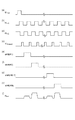
続いて、図15及び図16に基づいて、第1信号処理回路20及び第2信号処理回路30の動作について説明する。図15は、第1信号処理回路の動作を説明するためのタイミングチャートであり、図16は、第2信号処理回路の動作を説明するためのタイミングチャートである。
【0067】
図15において、制御回路から第1シフトレジスタ22にスタート信号ΦHstが入力されると、信号ΦH2の立ち上がりから信号ΦH1の立下りまでの期間に対応したパルス幅を有する信号shift(Hm)が順次出力される。第1シフトレジスタ22から対応する第1スイッチ素子21に信号shift(Hm)が出力されると、対応する第1スイッチ素子21が順次閉じ、対応する一方の光感応部分12mn群に蓄積された電荷が電流となって第1積分回路23に順次出力される。
【0068】
第1積分回路23には、制御回路からリセット信号ΦHresetが入力されており、リセット信号ΦHresetが「OFF」状態の期間、対応する一方の光感応部分12mn群に蓄積された電荷が容量素子25に蓄積されて、蓄積された電荷量に応じた電圧Houtが第1積分回路23から順次出力される。なお、第1積分回路23は、リセット信号ΦHresetが「ON」状態のときにはスイッチ素子26を閉じて容量素子25を初期化する。
【0069】
このように、第1信号処理回路20からは、第1の方向に配列された複数の画素1111〜111N,1121〜112N,・・・,11M1〜11MN間において電気的に接続された一方の光感応部分12mn群にて蓄積された電荷に対応した電圧Houtが、対応する一方の光感応部分12mn群毎に順次時系列データとして出力される。この時系列データは、図17(b)に示されるように、発光部3(発光素子)から照射され位置決めマーク像7(各マーク像7Y,7M,7C,7K)にて反射した光の第2の方向での輝度プロファイル(光強度分布)を示すものである。濃度検出用パターン9からの反射光の第2の方向での輝度プロファイルも、同様に検出される。なお、図17(a)は、位置決めマーク像7(各マーク像7Y,7M,7C,7K)を示している。
【0070】
図16において、制御回路から第2シフトレジスタ32にスタート信号ΦVstが入力されると、信号ΦV2の立ち上がりから信号ΦV1の立下りまでの期間に対応したパルス幅を有する信号shift(Vn)が順次出力される。第2シフトレジスタ32から対応する第2スイッチ素子31に信号shift(Vn)が出力されると、対応する第2スイッチ素子31が順次閉じ、対応する他方の光感応部分13mn群に蓄積された電荷が電流となって第2積分回路33に順次出力される。
【0071】
第2積分回路33には、制御回路からリセット信号ΦVresetが入力されており、リセット信号ΦVresetが「OFF」状態の期間、対応する他方の光感応部分13mn群に蓄積された電荷が容量素子35に蓄積されて、蓄積された電荷量に応じた電圧Voutが第2積分回路33から順次出力される。なお、第2積分回路33は、リセット信号ΦVresetが「ON」状態のときにはスイッチ素子36を閉じて容量素子35を初期化する。
【0072】
このように、第2信号処理回路30からは、第2の方向に配列された複数の画素1111〜11M1,1112〜11M2,・・・,111N〜11MN間において電気的に接続された他方の光感応部分13mn群にて蓄積された電荷に対応した電圧Voutが、対応する他方の光感応部分13mn群毎に順次時系列データとして出力される。この時系列データは、図17(c)に示されるように、発光部3(発光素子)から照射され位置決めマーク像7(各マーク像7Y,7M,7C,7K)にて反射した光の第1の方向での輝度プロファイル(光強度分布)を示すものである。濃度検出用パターン9からの反射光の第1の方向での輝度プロファイルも、同様に検出される。
【0073】
このように、本実施形態では、光検出部5において、1つの画素11mnに入射した光は当該画素11mnを構成する複数の光感応部分12mn,13mnそれぞれに、光強度に応じた電流が光感応部分12mn,13mn毎に出力される。そして、一方の光感応部分12mn同士が2次元配列における第1の方向に配列された複数の画素1111〜111N,1121〜112N,・・・,11M1〜11MNにわたって電気的に接続されているので、一方の光感応部分12mnから出力された電流は第1の方向に送られる。また、他方の光感応部分13mn同士が2次元配列における第2の方向に配列された複数の画素1111〜11M1,1112〜11M2,・・・,111N〜11MNにわたって電気的に接続されているので、他方の光感応部分13mnから出力された電流は第2の方向に送られる。このように、一方の光感応部分12mnから出力された電流は第1の方向に送られるとともに、他方の光感応部分13mnから出力された電流は第2の方向に送られることから、第1の方向での輝度プロファイルと第2の方向での輝度プロファイルとをそれぞれ独立して得ることが可能となる。この結果、1画素に複数の光感応部分12mn,13mnを配設するという極めて簡素な構成にて、位置決めマーク像7あるいは濃度検出用パターン9の第1の方向での輝度プロファイルと第2の方向での輝度プロファイルを高速に検出することができる。
【0074】
また、本実施形態において、各光感応部分12mn,13mnは、半導体基板40部分と第2導電型半導体領域41,42とを含み、第2導電型半導体領域41,42は、光入射方向から見て略三角形状を呈しており、1画素において互いに一辺が隣接して形成されている。これにより、複数の光感応部分12mn,13mnを1画素内に配設する際に、各光感応部分12mn,13mn(第2導電型半導体領域41,42)の面積が減少するのを抑制することができる。
【0075】
また、本実施形態において、第2導電型半導体領域41,42は、光入射方向から見て略長方形状を呈しており、1画素において長辺が隣接して形成されている。これにより、複数の光感応部分12mn,13mnを1画素内に配設する際に、各光感応部分12mn,13mn(第2導電型半導体領域41,42)の面積が減少するのを抑制することができる。
【0076】
また、本実施形態において、第2導電型半導体領域41,42は、光入射方向から見て4角形以上の多角形状を呈しており、1画素において1辺が隣接して形成されている。これにより、複数の光感応部分12mn,13mn(第2導電型半導体領域41,42)を1画素内に配設する際に、各光感応部分12mn,13mnの面積が減少するのを抑制することができる。また、各光感応部分12mn,13mnの面積に対する周囲長は減ることとなり、単位面積当たりに換算した暗電流が低減される。なお、4角形以上の多角形状として、菱形形状を採用してもよい。
【0077】
また、本実施形態において、第2導電型半導体領域41,42とは、1画素において第1の方向と第2の方向とに交差する第3の方向に並設されている。これにより、一方の光感応部分12mn群及び他方の光感応部分13mn群において、各光感応部分12mn,13mn群の中心部分に対応する光感応部分12mn,13mnが集中することとなり、解像度を向上することができる。
【0078】
また、第2導電型半導体領域41,42は、光入射方向から見てハニカム状に配列されている。これにより、複数の光感応部分12mn,13mn(第2導電型半導体領域41,42)を1画素内に配設する際に、各光感応部分12mn,13mnの面積が減少するのをより一層抑制することができる。また、幾何学的対称性が高く、第2導電型半導体領域41,42(光感応部分12mn,13mn)を形成するために用いるマスクが位置ずれしたことによる不均一性が抑制できる。
【0079】
また、本実施形態においては、第1配線44が、画素11mn間を第1の方向に延びて設けられており、第2配線47が、画素11mn間を第2の方向に延びて設けられている。これにより、それぞれの配線44,47により光感応部分12mn,13mn(第2導電型半導体領域41,42)への光の入射を妨げられることはなく、検出感度の低下を抑制できる。
【0080】
また、本実施形態においては、光検出部5が、第1シフトレジスタ22と、第2シフトレジスタ32と、第1積分回路23と、第2積分回路33とを有している。これにより、第1の方向での輝度プロファイルと第2の方向での輝度プロファイルとを極めて簡易な構成にて得ることができる。
【0081】
また、本実施形態においては、位置決めマーク像7あるいは濃度検出用パターン9の第1の方向での輝度プロファイルと第2の方向での輝度プロファイルの検出ためのデータ処理がm+n回(第1信号処理回路20においてm回のデータ処理、第2信号処理回路30においてn回のデータ処理)で済み、m×n画素を有するCCDイメージセンサを用いた場合のm×n回のデータ処理に比して、データ処理量が極めて少なくなる。この結果、第1信号処理回路20及び第2信号処理回路30における信号処理時間が短時間で済み、各信号処理回路20,30に対する負荷も小さくなる。
【0082】
また、本実施形態においては、カラーレーザビームプリンタ101(多重画像形成装置)が上記多重画像形成位置ずれ検出装置1(画像濃度検出装置)を備えている。これにより、カラーレーザビームプリンタ101は、1画素に複数の光感応部分12mn,13mnを配設するという極めて簡素な構成にて、位置決めマーク像7あるいは濃度検出用パターン9の第1の方向での輝度プロファイル及び第2の方向での輝度プロファイルを高速に検出することができる。
【0083】
本発明は、前述した実施形態に限定されるものではない。たとえば、シフトレジスタを用いる代わりに、各光感応部分12mn,13mn(第2導電型半導体領域41,42)を均一な抵抗線で接続して、光の入射に伴って発生した電荷を抵抗線に流れ込んだ位置と当該抵抗線それぞれの端部との距離に反比例するように抵抗分割して抵抗線の端部から取り出し、当該端部からの電流出力に基づいて光の入射位置を求めるようにしてもよい。
【0084】
また、前述した実施形態においては、1画素を複数の光感応部分で構成しているが、1画素を一つの光感応部分で構成してもよい。たとえば、図18に示されるように、光感応領域10は、第1の方向にわたって互いに電気的に接続される複数の第1光感応部分12mnと第2の方向にわたって互いに電気的に接続される複数の第2光感応部分13mnとを含み、複数の第1光感応部分12mnと複数の第2光感応部分13mnとは2次元的に混在した状態で同一面内にて配列してもよい。この場合、第1光感応部分12mnと第2光感応部分13mnとは市松模様状に配列しており、第1光感応部分12mnと第2光感応部分13mnとは第1の方向及び第2の方向において交互に配列している。なお、市松模様状に配列する代わりに、図12に示されるようなハニカム状に配列してもよい。
【0085】
また、本実施形態においては、多重画像形成位置ずれ検出装置と画像濃度検出装置とを共用しているが、これに限られることなく、多重画像形成位置ずれ検出装置と画像濃度検出装置とをそれぞれ独立して設けるように構成してもよい。また、本発明は、上述したカラーレーザビームプリンタ以外に、デジタルカラー複写機等の多重画像形成装置に適用することができる。
【0086】
【発明の効果】
以上、詳細に説明したとおり、本発明によれば、多重画像形成位置ずれ検出用パターンの検出処理の高速化および構成の簡素化を図ることができる多重画像形成位置ずれ検出装置を提供することができる。
【0087】
また、本発明によれば、濃度検出用パターンの検出処理の高速化および構成の簡素化を図ることができる画像濃度検出装置を提供することができる。
【0088】
また、本発明によれば、多重画像形成位置ずれ検出用パターンあるいは濃度検出用パターンの検出処理の高速化および構成の簡素化を図ることができる多重画像形成装置を提供することができる。
【図面の簡単な説明】
【図1】本実施形態に係る多重画像形成装置を示す概略構成図である。
【図2】本実施形態に係る多重画像形成装置に含まれる多重画像形成位置ずれ検出装置を示す概略構成図である。
【図3】図2に示された多重画像形成位置ずれ検出装置により、転写ベルト上に形成された多重画像形成位置ずれ検出用パターンとしての位置決めマーク像を検出するときの図である。
【図4】図2に示された多重画像形成位置ずれ検出装置により、転写ベルト上に形成された階調を有する濃度検出用パターンを検出するときの図である。
【図5】図2に示された多重画像形成位置ずれ検出装置に含まれる光検出部を示す概念構成図である。
【図6】図5に示された光検出部に含まれる光感応領域の一例を示す要部拡大平面図である。
【図7】図6のVII−VII線に沿った断面図である。
【図8】図5に示された光検出部に含まれる光感応領域の一例を示す要部拡大平面図である。
【図9】図5に示された光検出部に含まれる光感応領域の一例を示す要部拡大平面図である。
【図10】図5に示された光検出部に含まれる光感応領域の一例を示す要部拡大平面図である。
【図11】図5に示された光検出部に含まれる光感応領域の一例を示す要部拡大平面図である。
【図12】図5に示された光検出部に含まれる光感応領域の一例を示す要部拡大平面図である。
【図13】図5に示された光検出部に含まれる第1信号処理回路を示す概略構成図である。
【図14】図5に示された光検出部に含まれる第2信号処理回路を示す概略構成図である。
【図15】第1信号処理回路の動作を説明するためのタイミングチャートである。
【図16】第2信号処理回路の動作を説明するためのタイミングチャートである。
【図17】(a)は、多重画像形成位置ずれ検出用パターンとしての位置決めマーク像を示す図であり、(b)は、第1信号処理回路からの出力を説明するための線図であり、(c)は、第2信号処理回路からの出力を説明するための線図である。
【図18】図2に示された多重画像形成位置ずれ検出装置に含まれる光検出部の変形例を示す概念構成図である。
【符号の説明】
1…多重画像形成位置ずれ検出装置(画像濃度検出装置)、3…発光部、5…光検出部、7…位置決めマーク像(多重画像形成位置ずれ検出用パターン)、9…濃度検出用パターン、10…光感応領域、11mn…画素、12mn…一方の光感応部分、13mn…他方の光感応部分、20…第1信号処理回路、21…第1スイッチ素子、22…第1シフトレジスタ、23…第1積分回路、30…第2信号処理回路、31…第2スイッチ素子、32…第2シフトレジスタ、33…第2積分回路、101…カラーレーザビームプリンタ、102Y…イエロー用画像形成ステーション、102C…シアン用画像形成ステーション、102K…ブラック用画像形成ステーション、102M…マゼンタ用画像形成ステーション、107Y…イエロー用露光ユニット、107C…シアン用露光ユニット、107K…ブラック用露光ユニット、107M…マゼンタ用露光ユニット、110…転写ベルト、114Y…イエロー用転写ユニット、114C…シアン用転写ユニット、114K…ブラック用転写ユニット、114M…マゼンタ用転写ユニット。[0001]
TECHNICAL FIELD OF THE INVENTION
The present invention relates to a multiplex image forming position shift detecting device, an image density detecting device, and a multiplex image forming device.
[0002]
[Prior art]
As this type of multiplex image forming apparatus, a plurality of image forming units are arranged to form a multiplex image, each image of a different color is formed in each image forming unit, and the image is transferred to a transfer material and stacked. There has been known a technique in which a pattern (positioning pattern) for detecting a position shift of a multiplex image for correcting a shift of a transfer position of each image is read by a CCD image sensor (for example, see Patent Document 1). In
[0003]
[Patent Document 1]
JP-A-1-167770
[0004]
[Problems to be solved by the invention]
However, if a CCD image sensor is used to read the multiple image formation position shift detection pattern or the density detection pattern, the following problems occur. In the CCD image sensor, in order to obtain a light intensity distribution in one frame, data processing is required for all pixels (for example, when there are m × n pixels, data processing is performed m × n times). Time will be long. In addition, a signal processing circuit for performing data processing is required to have a higher performance and a higher speed.
[0005]
SUMMARY OF THE INVENTION The present invention has been made in view of the above-described circumstances, and a multiplex image forming position shift detecting device capable of speeding up a process of detecting a multiplex image forming position shift detecting pattern and simplifying a configuration. An image density detection device capable of speeding up the pattern detection processing and simplifying the configuration, and also speeding up the detection processing of the multiple image formation position shift detection pattern or the density detection pattern and simplifying the configuration. It is another object of the present invention to provide a multiplex image forming apparatus capable of performing the following.
[0006]
[Means for Solving the Problems]
A multiplex image forming position shift detecting device according to the present invention is a multiplex image forming position shift detecting pattern formed on a surface of a detection target in order to detect a transfer position shift of each image when forming a multiplex image. Is detected by light detection means having a light-sensitive area in which pixels are two-dimensionally arranged, the light detection means comprising: a plurality of light-emitting devices each outputting a current corresponding to the intensity of incident light. Are arranged adjacent to each other in the same plane to constitute one pixel, and a plurality of pixels constituting each pixel are arranged over a plurality of pixels arranged in a first direction in a two-dimensional array. One of the light-sensitive portions is electrically connected to each other, and the other of the plurality of light-sensitive portions constituting each pixel extends over a plurality of pixels arranged in the second direction in the two-dimensional array. The feeling of light Portions to each other is characterized by being electrically connected.
[0007]
In the multiplex image forming position shift detecting device according to the present invention, light incident on one pixel is detected in each of a plurality of light-sensitive portions constituting the pixel, and a current corresponding to light intensity is detected by the light detecting means. Output for each sensitive part. Since one of the photosensitive portions is electrically connected to a plurality of pixels arranged in the first direction in the two-dimensional array, the current output from the one photosensitive portion is transmitted in the first direction. Can be In addition, since the other photosensitive portions are electrically connected to each other over a plurality of pixels arranged in the second direction in the two-dimensional array, the current output from the other photosensitive portion is transmitted in the second direction. Can be Thus, while the current output from one photosensitive portion is sent in the first direction and the current output from the other photosensitive portion is sent in the second direction, the brightness in the first direction The profile and the luminance profile in the second direction can be obtained independently of each other. As a result, the luminance profile in the first direction and the luminance profile in the second direction of the multiple image formation position shift detection pattern can be changed with a very simple configuration in which a plurality of light-sensitive portions are arranged in one pixel. It can be detected at high speed.
[0008]
The image density detection device according to the present invention is configured to detect a density of an image by using a density detection pattern formed on a surface of a detection target by a light detection unit having a light-sensitive region in which pixels are two-dimensionally arranged. An image density detection device for detecting, wherein the light detection means comprises a plurality of light-sensitive portions which respectively output currents according to the intensity of incident light, and are arranged adjacent to each other in the same plane, so that one pixel is formed. A plurality of pixels arranged in the first direction in the two-dimensional array, one of the plurality of photosensitive portions constituting each pixel is electrically connected to each other, and Over a plurality of pixels arranged in the second direction in the arrangement, the other light-sensitive portions of the plurality of light-sensitive portions constituting each pixel are electrically connected to each other.
[0009]
In the image density detecting device according to the present invention, the light incident on one pixel is detected in each of the plurality of light-sensitive portions constituting the pixel by the light detection means, and a current corresponding to the light intensity is output for each light-sensitive portion. Is output to Since one of the photosensitive portions is electrically connected to a plurality of pixels arranged in the first direction in the two-dimensional array, the current output from the one photosensitive portion is transmitted in the first direction. Can be In addition, since the other photosensitive portions are electrically connected to each other over a plurality of pixels arranged in the second direction in the two-dimensional array, the current output from the other photosensitive portion is transmitted in the second direction. Can be Thus, while the current output from one photosensitive portion is sent in the first direction and the current output from the other photosensitive portion is sent in the second direction, the brightness in the first direction The profile and the luminance profile in the second direction can be obtained independently of each other. As a result, the luminance profile in the first direction and the luminance profile in the second direction of the density detection pattern are detected at high speed with a very simple configuration in which a plurality of light-sensitive portions are arranged in one pixel. be able to.
[0010]
Further, the light detecting means reads an output from one of the light-sensitive sub-groups electrically connected between the plurality of pixels arranged in the first direction, and reads a second output in the two-dimensional array based on the output. And a first signal processing circuit for detecting a luminance profile in the direction of the second direction, and an output from the other photosensitive group electrically connected between the plurality of pixels arranged in the second direction and reading the output. And a second signal processing circuit that detects a luminance profile in a first direction in the two-dimensional array based on the second signal processing circuit.
[0011]
A multiplex image forming apparatus according to the present invention includes: a plurality of image forming units that form different images to form a multiplex image; and the multiplex image forming position shift detecting device. , The shift of the transfer position of each image formed is detected by the multiple image forming position shift detecting device.
[0012]
Since the multiplex image forming apparatus according to the present invention includes the multiplex image forming position shift detecting device, the multiplex image forming position shift detecting method can be performed with a very simple configuration in which a plurality of light-sensitive portions are disposed in one pixel. A luminance profile in the first direction and a luminance profile in the second direction of the use pattern can be detected at high speed.
[0013]
A multiplex image forming apparatus according to the present invention includes a plurality of image forming units that form different images to form a multiplex image, and the image density detecting device, respectively. It is characterized in that the density of each of the obtained images is detected by an image density detecting device.
[0014]
Since the multiplex image forming apparatus according to the present invention includes the above-described image density detecting device, the multiplex image forming apparatus has a very simple configuration in which a plurality of light-sensitive portions are provided in one pixel, and the first direction of the density detecting pattern And the luminance profile in the second direction can be detected at high speed.
[0015]
BEST MODE FOR CARRYING OUT THE INVENTION
An embodiment according to the present invention will be described with reference to the drawings. In the description, the same elements or elements having the same functions will be denoted by the same reference symbols, without redundant description. Hereinafter, each of the parameters M and N is an integer of 2 or more. Unless otherwise specified, the parameter m is any integer from 1 to M, and the parameter n is any integer from 1 to N.
[0016]
FIG. 1 is a schematic configuration diagram showing a multiplex image forming apparatus according to the present embodiment, and corresponds to, for example, a four-drum type color laser beam printer. The multiplex image forming apparatus according to the present embodiment includes the multiplex image forming position shift detecting apparatus and the image density detecting apparatus according to the embodiment of the present invention.
[0017]
The color laser beam printer 101 (multiplex image forming apparatus) includes a yellow image forming station 102Y, a magenta
[0018]
The yellow image forming station 102Y is provided with a cleaner 103Y, a charger 104Y, a developing unit 105Y, and a photosensitive drum 106Y as an image carrier. A
[0019]
The magenta
[0020]
The cyan
[0021]
The black image forming station 102K includes a cleaner 103K, a
[0022]
A
[0023]
The transfer paper Pa as a sheet is stored in a plurality of
[0024]
The transfer paper Pa on which the respective color images are fixed by the fixing unit 120 is discharged to the outside of the color
[0025]
As described above, when forming an image in the color
[0026]
As shown in FIG. 3, the
[0027]
As shown in FIG. 2, the
[0028]
The
[0029]
At this time, the detection of the
[0030]
In this manner, the reflected light detected by the
[0031]
In accordance with the amount of deviation, the reflecting mirrors in the laser beam paths of the laser scanning means 108Y, 108M, 108C and 108K are operated using a stepping motor (not shown), and magnification, inclination in the sub-scanning direction, parallel movement, etc. Is adjusted to adjust the registration. Note that, in addition to the above, the deviation amount of the registration can be corrected by controlling the driving of the photosensitive drum and the transfer belt. In addition, in addition to the above, the amount of registration deviation can be corrected by moving the relative position between the
[0032]
In this registration correction, one of the color
[0033]
Here, it is assumed that the
[0034]
Next, reading (detection) of a density detection pattern formed on the
[0035]
First, the detection of the density detection pattern is performed separately from the detection of the positioning mark image at the time of registration correction. As shown in FIG. 4, when printing the
[0036]
The transfer of the
[0037]
The output value of the density detection pattern detected by the
[0038]
The above-described registration correction and image density control are separate operations, and the timing at which each operation is performed is such that the amount of registration deviation of each color is always within a predetermined range for registration correction. And the density control of the image is performed such that the density or gradation of the image of each color is kept constant. As described above, the printing operation is performed in a state where there is no transfer deviation due to the registration correction, and in a state where the density and gradation of the image of each color are properly maintained by the image density control.
[0039]
Next, the
[0040]
The
[0041]
A plurality of
[0042]
Here, the configuration of the
[0043]
The
[0044]
A first insulating
[0045]
A second insulating
[0046]
On the second insulating
[0047]
The
[0048]
The
[0049]
Further, in the light-
[0050]
The shape of the
[0051]
The second-conductivity-type semiconductor region (light-sensitive portion) shown in FIG. 8 has a rectangular shape when viewed from the light incident direction, and two
[0052]
In the second conductivity type semiconductor region (light sensitive portion) shown in FIG. 9, one
[0053]
The second conductivity type semiconductor region (light sensitive portion) shown in FIG. 10 is composed of four
[0054]
The second conductivity type semiconductor region (light sensitive portion) shown in FIG. 11 is formed so that two comb-shaped
[0055]
The second-conductivity-type semiconductor region (light-sensitive portion) shown in FIG. 12 has a polygonal shape (for example, an octagonal shape) of a quadrangle or more when viewed from the light incident direction, and one side is adjacent to one pixel. It is formed. The
[0056]
Subsequently, the configurations of the first
[0057]
The first
[0058]
As shown in FIG. 13, the first
[0059]
The
[0060]
The first integrating
[0061]
When the
[0062]
As shown in FIG. 14, the second
[0063]
The
[0064]
The second integrating
[0065]
When the
[0066]
Subsequently, the operation of the first
[0067]
In FIG. 15, the control circuit sends a start signal Φ to the
[0068]
The first integrating
[0069]
As described above, the first
[0070]
In FIG. 16, the control circuit sends a start signal Φ to the
[0071]
The second integrating
[0072]
As described above, the second
[0073]
As described above, in the present embodiment, one
[0074]
Further, in the present embodiment, each light-sensitive portion 12 mn , 13 mn Includes a
[0075]
In the present embodiment, the second conductivity
[0076]
In the present embodiment, the second conductivity
[0077]
In the present embodiment, the second conductivity
[0078]
The second conductivity
[0079]
In the present embodiment, the
[0080]
In the present embodiment, the
[0081]
In the present embodiment, data processing for detecting the luminance profile in the first direction and the luminance profile in the second direction of the
[0082]
In the present embodiment, the color laser beam printer 101 (multiplex image forming apparatus) includes the above-described multiple image forming position shift detecting device 1 (image density detecting device). This allows the color
[0083]
The present invention is not limited to the embodiments described above. For example, instead of using a shift register, each light sensitive portion 12 mn , 13 mn (Second conductivity
[0084]
Further, in the above-described embodiment, one pixel is constituted by a plurality of photosensitive parts, but one pixel may be constituted by one photosensitive part. For example, as shown in FIG. 18, the
[0085]
Further, in the present embodiment, the multiplex image forming position shift detecting device and the image density detecting device are shared, but the present invention is not limited to this. You may comprise so that it may be provided independently. Further, the present invention can be applied to a multiplex image forming apparatus such as a digital color copying machine in addition to the above-described color laser beam printer.
[0086]
【The invention's effect】
As described above in detail, according to the present invention, it is possible to provide a multiplex image forming position shift detecting device capable of speeding up the process of detecting a multiplex image forming position shift detecting pattern and simplifying the configuration. it can.
[0087]
Further, according to the present invention, it is possible to provide an image density detection device capable of speeding up the process of detecting a pattern for density detection and simplifying the configuration.
[0088]
Further, according to the present invention, it is possible to provide a multiplex image forming apparatus capable of speeding up the detection processing of the multiplex image formation position shift detection pattern or the density detection pattern and simplifying the configuration.
[Brief description of the drawings]
FIG. 1 is a schematic configuration diagram illustrating a multiplex image forming apparatus according to an embodiment.
FIG. 2 is a schematic configuration diagram illustrating a multiplex image forming position deviation detecting device included in the multiplex image forming device according to the present embodiment.
FIG. 3 is a diagram when a positioning mark image as a multiplex image forming position shift detection pattern formed on a transfer belt is detected by the multiplex image forming position shift detecting device shown in FIG. 2;
FIG. 4 is a diagram when the multiple image forming position deviation detecting device shown in FIG. 2 detects a density detecting pattern having a gradation formed on a transfer belt.
FIG. 5 is a conceptual configuration diagram illustrating a light detection unit included in the multiple image formation position shift detection device illustrated in FIG. 2;
FIG. 6 is an enlarged plan view of a main part showing an example of a light sensitive area included in the light detection unit shown in FIG.
FIG. 7 is a sectional view taken along line VII-VII in FIG.
FIG. 8 is an enlarged plan view of a main part showing an example of a light sensitive area included in the light detection unit shown in FIG.
9 is an enlarged plan view of a main part showing an example of a light-sensitive area included in the light detection unit shown in FIG.
FIG. 10 is an enlarged plan view of a main part showing an example of a light-sensitive region included in the light detection unit shown in FIG.
FIG. 11 is an enlarged plan view of a main part showing an example of a light-sensitive area included in the light detection unit shown in FIG.
12 is a main part enlarged plan view showing an example of a light-sensitive area included in the light detection unit shown in FIG.
FIG. 13 is a schematic configuration diagram illustrating a first signal processing circuit included in the photodetector illustrated in FIG. 5;
FIG. 14 is a schematic configuration diagram illustrating a second signal processing circuit included in the photodetector illustrated in FIG. 5;
FIG. 15 is a timing chart for explaining the operation of the first signal processing circuit.
FIG. 16 is a timing chart for explaining the operation of the second signal processing circuit.
17A is a diagram showing a positioning mark image as a pattern for detecting a position shift of a multiplex image formation, and FIG. 17B is a diagram for explaining an output from a first signal processing circuit; (C) is a diagram for explaining an output from the second signal processing circuit.
FIG. 18 is a conceptual configuration diagram illustrating a modified example of a light detection unit included in the multiple image formation position shift detection device illustrated in FIG. 2;
[Explanation of symbols]
DESCRIPTION OF
Claims (6)
前記光検出手段は、
各々入射した光の強度に応じた電流を出力する複数の光感応部分を同一面内にて隣接して配設することで1画素が構成されており、
前記2次元配列における第1の方向に配列された複数の画素にわたって、当該各画素を構成する複数の光感応部分のうち一方の光感応部分同士が電気的に接続され、
前記2次元配列における第2の方向に配列された複数の画素にわたって、当該各画素を構成する複数の光感応部分のうち他方の光感応部分同士が電気的に接続されていることを特徴とする多重画像形成位置ずれ検出装置。In order to detect a shift in the transfer position of each image when forming a multiplex image, a multiplex image formation position shift detection pattern formed on the surface of the detection target is defined by a light-sensitive area in which pixels are two-dimensionally arranged. A multiplex image forming position shift detecting device for detecting by a light detecting means,
The light detection means,
One pixel is configured by arranging a plurality of light-sensitive portions that respectively output currents according to the intensity of incident light adjacent to each other in the same plane,
Over a plurality of pixels arranged in the first direction in the two-dimensional array, one of the plurality of photosensitive portions constituting each pixel is electrically connected to each other,
Over a plurality of pixels arranged in the second direction in the two-dimensional array, the other photosensitive portion of the plurality of photosensitive portions constituting each pixel is electrically connected to each other. Multiple image forming position shift detecting device.
前記第1の方向に配列された前記複数の画素間において電気的に接続された一方の光感応部分群からの出力を読み出して当該出力に基づいて前記2次元配列における前記第2の方向での輝度プロファイルを検出する第1信号処理回路と、
前記第2の方向に配列された前記複数の画素間において電気的に接続された他方の光感応部分群からの出力を読み出して当該出力に基づいて前記2次元配列における前記第1の方向での輝度プロファイルを検出する第2信号処理回路と、を有することを特徴とする請求項1に記載の多重画像形成位置ずれ検出装置。The light detection means,
An output from one of the light-sensitive sub-groups electrically connected between the plurality of pixels arranged in the first direction is read out, and based on the output, the output in the second direction in the two-dimensional array is read out. A first signal processing circuit for detecting a luminance profile;
An output from the other photosensitive sub-group electrically connected between the plurality of pixels arranged in the second direction is read out, and based on the output, the output in the first direction in the two-dimensional arrangement is read out. The apparatus according to claim 1, further comprising a second signal processing circuit that detects a luminance profile.
前記光検出手段は、
各々入射した光の強度に応じた電流を出力する複数の光感応部分を同一面内にて隣接して配設することで1画素が構成されており、
前記2次元配列における第1の方向に配列された複数の画素にわたって、当該各画素を構成する複数の光感応部分のうち一方の光感応部分同士が電気的に接続され、
前記2次元配列における第2の方向に配列された複数の画素にわたって、当該各画素を構成する複数の光感応部分のうち他方の光感応部分同士が電気的に接続されていることを特徴とする画像濃度検出装置。An image density detection device for detecting a density detection pattern formed on a surface of a detection target by a light detection unit having a photosensitive region in which pixels are two-dimensionally arranged, in order to detect a density of an image,
The light detection means,
One pixel is configured by arranging a plurality of light-sensitive portions that respectively output currents according to the intensity of incident light adjacent to each other in the same plane,
Over a plurality of pixels arranged in the first direction in the two-dimensional array, one of the plurality of photosensitive portions constituting each pixel is electrically connected to each other,
Over a plurality of pixels arranged in the second direction in the two-dimensional array, the other photosensitive portion of the plurality of photosensitive portions constituting each pixel is electrically connected to each other. Image density detection device.
前記第1の方向に配列された前記複数の画素間において電気的に接続された一方の光感応部分群からの出力を読み出して当該出力に基づいて前記2次元配列における前記第2の方向での輝度プロファイルを検出する第1信号処理回路と、
前記第2の方向に配列された前記複数の画素間において電気的に接続された他方の光感応部分群からの出力を読み出して当該出力に基づいて前記2次元配列における前記第1の方向での輝度プロファイルを検出する第2信号処理回路と、を有することを特徴とする請求項3に記載の画像濃度検出装置。The light detection means,
An output from one of the light-sensitive sub-groups electrically connected between the plurality of pixels arranged in the first direction is read out, and based on the output, the output in the second direction in the two-dimensional array is read out. A first signal processing circuit for detecting a luminance profile;
An output from the other photosensitive sub-group electrically connected between the plurality of pixels arranged in the second direction is read out, and based on the output, the output in the first direction in the two-dimensional arrangement is read out. The image density detection device according to claim 3, further comprising a second signal processing circuit that detects a luminance profile.
請求項1に記載の多重画像形成位置ずれ検出装置と、を備え、
前記画像形成部によりそれぞれ形成された各画像の転写位置のずれを前記多重画像形成位置ずれ検出装置により検出することを特徴とする多重画像形成装置。A plurality of image forming units each forming a different image to form a multiplex image,
And a multiplex image forming position shift detecting device according to claim 1.
A multiplex image forming apparatus, wherein a shift of a transfer position of each image formed by the image forming unit is detected by the multiplex image forming position shift detecting device.
請求項3に記載の画像濃度検出装置と、を備え、
前記画像形成部によりそれぞれ形成された各画像の濃度を前記画像濃度検出装置により検出することを特徴とする多重画像形成装置。A plurality of image forming units each forming a different image to form a multiplex image,
An image density detection device according to claim 3,
A multiplex image forming apparatus, wherein the density of each image formed by the image forming unit is detected by the image density detecting device.
Priority Applications (7)
| Application Number | Priority Date | Filing Date | Title |
|---|---|---|---|
| JP2003016559A JP2004264332A (en) | 2003-01-24 | 2003-01-24 | Multiple image forming position shift detecting device, image density detecting device, and multiple image forming device |
| TW093101453A TWI301557B (en) | 2003-01-24 | 2004-01-20 | Offset detector for foming position of multiple image, image density detector, and device for forming multiple image |
| KR1020057013451A KR20050094456A (en) | 2003-01-24 | 2004-01-22 | Multiple image formation position shift detection device, image concentrationn detection device, and multiple image formation device |
| CNB2004800027348A CN100405230C (en) | 2003-01-24 | 2004-01-22 | Multiple image forming position deviation detecting device, image density detecting device, and multiple image forming apparatus |
| PCT/JP2004/000551 WO2004066032A1 (en) | 2003-01-24 | 2004-01-22 | Multiple image formation position shift detection device, image concentration detection device, and multiple image formation device |
| EP04704339A EP1589382A4 (en) | 2003-01-24 | 2004-01-22 | MULTI-IMAGE FORMATION POSITION SHIFT DETECTION DEVICE, IMAGE CONCENTRATION DETECTION DEVICE AND MULTI-IMAGE FORMING DEVICE |
| US10/542,861 US20060239587A1 (en) | 2003-01-24 | 2004-01-22 | Multiple image formation position shift detection device, image concentration detection device, and multiple image formation device |
Applications Claiming Priority (1)
| Application Number | Priority Date | Filing Date | Title |
|---|---|---|---|
| JP2003016559A JP2004264332A (en) | 2003-01-24 | 2003-01-24 | Multiple image forming position shift detecting device, image density detecting device, and multiple image forming device |
Publications (1)
| Publication Number | Publication Date |
|---|---|
| JP2004264332A true JP2004264332A (en) | 2004-09-24 |
Family
ID=32767481
Family Applications (1)
| Application Number | Title | Priority Date | Filing Date |
|---|---|---|---|
| JP2003016559A Pending JP2004264332A (en) | 2003-01-24 | 2003-01-24 | Multiple image forming position shift detecting device, image density detecting device, and multiple image forming device |
Country Status (7)
| Country | Link |
|---|---|
| US (1) | US20060239587A1 (en) |
| EP (1) | EP1589382A4 (en) |
| JP (1) | JP2004264332A (en) |
| KR (1) | KR20050094456A (en) |
| CN (1) | CN100405230C (en) |
| TW (1) | TWI301557B (en) |
| WO (1) | WO2004066032A1 (en) |
Families Citing this family (2)
| Publication number | Priority date | Publication date | Assignee | Title |
|---|---|---|---|---|
| US9635287B2 (en) * | 2011-10-11 | 2017-04-25 | Raytheon Company | Method and apparatus for integrated sensor to provide higher resolution, lower frame rate and lower resolution, higher frame rate imagery simultaneously |
| CN105035557B (en) * | 2015-08-06 | 2017-03-22 | 京东方科技集团股份有限公司 | Substrate cartridge |
Family Cites Families (29)
| Publication number | Priority date | Publication date | Assignee | Title |
|---|---|---|---|---|
| JPS59166208U (en) * | 1983-04-20 | 1984-11-07 | オムロン株式会社 | Photosensor for optical fiber coupling |
| JPH0610699Y2 (en) * | 1986-07-03 | 1994-03-16 | 三洋電機株式会社 | Light receiving device |
| US5854482A (en) * | 1992-10-05 | 1998-12-29 | Logitech, Inc. | Pointing device utilizing a photodector array |
| US5907152A (en) * | 1992-10-05 | 1999-05-25 | Logitech, Inc. | Pointing device utilizing a photodetector array |
| US5703356A (en) * | 1992-10-05 | 1997-12-30 | Logitech, Inc. | Pointing device utilizing a photodetector array |
| DE69421747T2 (en) * | 1993-04-30 | 2000-05-11 | Sharp Kk | Board with integrated display with high coordinate detection accuracy and method for its control |
| JPH0736230A (en) * | 1993-07-16 | 1995-02-07 | Mita Ind Co Ltd | Image density control method |
| US5699450A (en) * | 1995-02-28 | 1997-12-16 | Xerox Corporation | Detector array method and apparatus for real time in situ color control in printers and copiers |
| US6256016B1 (en) * | 1997-06-05 | 2001-07-03 | Logitech, Inc. | Optical detection system, device, and method utilizing optical matching |
| KR19990015277A (en) * | 1997-08-04 | 1999-03-05 | 윤종용 | Color registration correction method in the image forming apparatus |
| JP4812940B2 (en) * | 1998-10-30 | 2011-11-09 | 浜松ホトニクス株式会社 | Solid-state imaging device array |
| KR100344505B1 (en) * | 1998-11-30 | 2002-07-24 | 가부시끼가이샤 도시바 | Solid-state imaging device |
| JP2000253315A (en) * | 1999-03-01 | 2000-09-14 | Kawasaki Steel Corp | CMOS image sensor |
| JP2001196868A (en) * | 2000-01-13 | 2001-07-19 | Sony Corp | Amplifier and wireless communication device using the same |
| JP4387546B2 (en) * | 2000-03-22 | 2009-12-16 | 株式会社リコー | CAMERA, IMAGE INPUT DEVICE, MOBILE TERMINAL DEVICE, AND CAMERA FORM CHANGE METHOD |
| JP3882507B2 (en) * | 2000-05-19 | 2007-02-21 | カシオ電子工業株式会社 | Color image forming apparatus |
| US6275244B1 (en) * | 2000-09-14 | 2001-08-14 | Xerox Corporation | Color printing image bearing member color registration system |
| US6747290B2 (en) * | 2000-12-12 | 2004-06-08 | Semiconductor Energy Laboratory Co., Ltd. | Information device |
| US6642495B2 (en) * | 2001-02-12 | 2003-11-04 | Princeton Scientific Instruments | Optical pulse counting imager and system |
| JP4810763B2 (en) * | 2001-06-20 | 2011-11-09 | 株式会社デンソー | Distance measuring device |
| TWI263942B (en) * | 2001-12-05 | 2006-10-11 | Em Microelectronic Marin Sa | Method and sensing device for motion detection in an optical pointing device, such as an optical mouse |
| CN100394606C (en) * | 2001-12-05 | 2008-06-11 | 浜松光子学株式会社 | Light detection device, imaging device and ranging image capture device |
| JP3965049B2 (en) * | 2001-12-21 | 2007-08-22 | 浜松ホトニクス株式会社 | Imaging device |
| US6763199B2 (en) * | 2002-01-16 | 2004-07-13 | Xerox Corporation | Systems and methods for one-step setup for image on paper registration |
| US6684773B2 (en) * | 2002-03-21 | 2004-02-03 | Lexmark International, Inc. | Target and algorithm for color laser printhead alignment |
| EP1586856B1 (en) * | 2003-01-22 | 2013-01-09 | Hamamatsu Photonics K.K. | Optical sensing device |
| JP2004264034A (en) * | 2003-01-24 | 2004-09-24 | Hamamatsu Photonics Kk | Photodetector |
| JP4099413B2 (en) * | 2003-03-20 | 2008-06-11 | 浜松ホトニクス株式会社 | Photodetector |
| WO2005015132A1 (en) * | 2003-08-06 | 2005-02-17 | Hamamatsu Photonics K.K. | Absolute encoder |
-
2003
- 2003-01-24 JP JP2003016559A patent/JP2004264332A/en active Pending
-
2004
- 2004-01-20 TW TW093101453A patent/TWI301557B/en not_active IP Right Cessation
- 2004-01-22 EP EP04704339A patent/EP1589382A4/en not_active Withdrawn
- 2004-01-22 US US10/542,861 patent/US20060239587A1/en not_active Abandoned
- 2004-01-22 WO PCT/JP2004/000551 patent/WO2004066032A1/en not_active Ceased
- 2004-01-22 KR KR1020057013451A patent/KR20050094456A/en not_active Ceased
- 2004-01-22 CN CNB2004800027348A patent/CN100405230C/en not_active Expired - Fee Related
Also Published As
| Publication number | Publication date |
|---|---|
| TWI301557B (en) | 2008-10-01 |
| US20060239587A1 (en) | 2006-10-26 |
| TW200416478A (en) | 2004-09-01 |
| EP1589382A1 (en) | 2005-10-26 |
| CN100405230C (en) | 2008-07-23 |
| EP1589382A4 (en) | 2008-03-19 |
| KR20050094456A (en) | 2005-09-27 |
| WO2004066032A1 (en) | 2004-08-05 |
| CN1742240A (en) | 2006-03-01 |
Similar Documents
| Publication | Publication Date | Title |
|---|---|---|
| US7045773B2 (en) | Optical scanning apparatus for accurately detecting and correcting position of optical beam in subscanning direction, and the method | |
| US10901338B2 (en) | Image forming apparatus with photosensitive drum exposed by linearly-arranged light emission elements having an overlap | |
| US20030044190A1 (en) | Image forming apparatus and patch detection method | |
| US11016407B2 (en) | Image forming apparatus | |
| US9213290B2 (en) | Image forming apparatus capable of changing the number of light receiving elements of a light receiving unit | |
| JP5817764B2 (en) | Optical writing apparatus and image forming apparatus | |
| JP5862404B2 (en) | Light emitting element array chip, light emitting element head, and image forming apparatus | |
| JP7567318B2 (en) | Image forming device | |
| WO2020004484A1 (en) | Image forming device | |
| US20210117739A1 (en) | Image forming apparatus | |
| US20200225600A1 (en) | Image forming apparatus | |
| CN114475012B (en) | Light emitting device, light emitting element array chip, and exposure device | |
| JP2004264332A (en) | Multiple image forming position shift detecting device, image density detecting device, and multiple image forming device | |
| US11194265B2 (en) | Image forming apparatus | |
| CN108540737A (en) | Photoelectric conversion device, sensor unit and image forming apparatus | |
| JP5866924B2 (en) | Light emitting element head and image forming apparatus | |
| JP2006264173A (en) | Image forming device | |
| JP5824993B2 (en) | Image forming apparatus and light emitting element head | |
| JP7505348B2 (en) | Light emitting element head and image forming apparatus | |
| JP4896506B2 (en) | Optical scanning apparatus and image forming apparatus | |
| JP5568931B2 (en) | Light emitting element array and image forming apparatus using the same | |
| JP2019102633A (en) | Light emitting device array and exposure head using the same, and image forming apparatus | |
| JP2019181728A (en) | Optical writing device and image formation apparatus | |
| JPH1184282A (en) | Image forming device | |
| JP2001083640A (en) | Method and device for reading image information |