JP2004266253A - 電子部品用基板 - Google Patents
電子部品用基板 Download PDFInfo
- Publication number
- JP2004266253A JP2004266253A JP2003409463A JP2003409463A JP2004266253A JP 2004266253 A JP2004266253 A JP 2004266253A JP 2003409463 A JP2003409463 A JP 2003409463A JP 2003409463 A JP2003409463 A JP 2003409463A JP 2004266253 A JP2004266253 A JP 2004266253A
- Authority
- JP
- Japan
- Prior art keywords
- insulating base
- circuit board
- flexible circuit
- electronic component
- component substrate
- Prior art date
- Legal status (The legal status is an assumption and is not a legal conclusion. Google has not performed a legal analysis and makes no representation as to the accuracy of the status listed.)
- Granted
Links
- 239000000758 substrate Substances 0.000 title claims abstract description 85
- 239000004020 conductor Substances 0.000 claims abstract description 19
- 229920003002 synthetic resin Polymers 0.000 claims abstract description 19
- 239000000057 synthetic resin Substances 0.000 claims abstract description 19
- 238000005229 chemical vapour deposition Methods 0.000 claims abstract description 14
- 229910052751 metal Inorganic materials 0.000 claims abstract description 14
- 239000002184 metal Substances 0.000 claims abstract description 14
- 238000005240 physical vapour deposition Methods 0.000 claims abstract description 14
- 239000010409 thin film Substances 0.000 claims abstract description 14
- 239000010408 film Substances 0.000 claims abstract description 9
- 239000000463 material Substances 0.000 claims description 14
- 238000000465 moulding Methods 0.000 claims description 12
- 230000002093 peripheral effect Effects 0.000 claims description 10
- PXHVJJICTQNCMI-UHFFFAOYSA-N Nickel Chemical compound [Ni] PXHVJJICTQNCMI-UHFFFAOYSA-N 0.000 claims description 6
- 238000003825 pressing Methods 0.000 claims description 5
- 239000011195 cermet Substances 0.000 claims description 3
- 229910052759 nickel Inorganic materials 0.000 claims description 3
- 229910052715 tantalum Inorganic materials 0.000 claims description 3
- GUVRBAGPIYLISA-UHFFFAOYSA-N tantalum atom Chemical compound [Ta] GUVRBAGPIYLISA-UHFFFAOYSA-N 0.000 claims description 3
- 238000004519 manufacturing process Methods 0.000 abstract description 17
- 238000010586 diagram Methods 0.000 abstract description 8
- 229920005989 resin Polymers 0.000 description 18
- 239000011347 resin Substances 0.000 description 18
- 239000000919 ceramic Substances 0.000 description 17
- 238000003780 insertion Methods 0.000 description 8
- 230000037431 insertion Effects 0.000 description 8
- OKTJSMMVPCPJKN-UHFFFAOYSA-N Carbon Chemical compound [C] OKTJSMMVPCPJKN-UHFFFAOYSA-N 0.000 description 3
- 239000004734 Polyphenylene sulfide Substances 0.000 description 3
- 229910052799 carbon Inorganic materials 0.000 description 3
- 238000000034 method Methods 0.000 description 3
- 229920000069 polyphenylene sulfide Polymers 0.000 description 3
- 238000007740 vapor deposition Methods 0.000 description 3
- VYZAMTAEIAYCRO-UHFFFAOYSA-N Chromium Chemical compound [Cr] VYZAMTAEIAYCRO-UHFFFAOYSA-N 0.000 description 2
- 239000004677 Nylon Substances 0.000 description 2
- BPQQTUXANYXVAA-UHFFFAOYSA-N Orthosilicate Chemical compound [O-][Si]([O-])([O-])[O-] BPQQTUXANYXVAA-UHFFFAOYSA-N 0.000 description 2
- KJTLSVCANCCWHF-UHFFFAOYSA-N Ruthenium Chemical compound [Ru] KJTLSVCANCCWHF-UHFFFAOYSA-N 0.000 description 2
- 229910052804 chromium Inorganic materials 0.000 description 2
- 239000011651 chromium Substances 0.000 description 2
- 150000001875 compounds Chemical class 0.000 description 2
- 230000000694 effects Effects 0.000 description 2
- 238000010304 firing Methods 0.000 description 2
- 239000011521 glass Substances 0.000 description 2
- 239000000203 mixture Substances 0.000 description 2
- 229920001778 nylon Polymers 0.000 description 2
- 229910052707 ruthenium Inorganic materials 0.000 description 2
- 229920001169 thermoplastic Polymers 0.000 description 2
- 239000004416 thermosoftening plastic Substances 0.000 description 2
- RYGMFSIKBFXOCR-UHFFFAOYSA-N Copper Chemical compound [Cu] RYGMFSIKBFXOCR-UHFFFAOYSA-N 0.000 description 1
- 229910004298 SiO 2 Inorganic materials 0.000 description 1
- 229910052802 copper Inorganic materials 0.000 description 1
- 239000010949 copper Substances 0.000 description 1
- 238000005520 cutting process Methods 0.000 description 1
- PCHJSUWPFVWCPO-UHFFFAOYSA-N gold Chemical compound [Au] PCHJSUWPFVWCPO-UHFFFAOYSA-N 0.000 description 1
- 229910052737 gold Inorganic materials 0.000 description 1
- 239000010931 gold Substances 0.000 description 1
- 238000002347 injection Methods 0.000 description 1
- 239000007924 injection Substances 0.000 description 1
- 238000009413 insulation Methods 0.000 description 1
- 238000010884 ion-beam technique Methods 0.000 description 1
- 238000001465 metallisation Methods 0.000 description 1
- 238000012986 modification Methods 0.000 description 1
- 230000004048 modification Effects 0.000 description 1
- 229910001120 nichrome Inorganic materials 0.000 description 1
- 229910000623 nickel–chromium alloy Inorganic materials 0.000 description 1
- 238000005268 plasma chemical vapour deposition Methods 0.000 description 1
- 229920001721 polyimide Polymers 0.000 description 1
- 239000000843 powder Substances 0.000 description 1
- 238000004544 sputter deposition Methods 0.000 description 1
- MZLGASXMSKOWSE-UHFFFAOYSA-N tantalum nitride Chemical compound [Ta]#N MZLGASXMSKOWSE-UHFFFAOYSA-N 0.000 description 1
- 238000002230 thermal chemical vapour deposition Methods 0.000 description 1
- 238000001771 vacuum deposition Methods 0.000 description 1
Images


Landscapes
- Adjustable Resistors (AREA)
Abstract
【解決手段】 絶縁基台10と、絶縁基台10上に取り付けられる合成樹脂フイルム上に端子パターン29,29とその表面に摺動子が摺接する導体パターン25とを設けてなるフレキシブル基板20とを具備して電子部品用基板1−1を構成する。導体パターン25を物理的蒸着又は化学的蒸着による金属薄膜によって構成する。絶縁基台10は合成樹脂成形品であり、フレキシブル基板20は絶縁基台10にインサート成形される。
【選択図】 図1
Description
〔第一の実施の形態〕
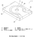
図1,図2は本発明の第一の実施の形態にかかる電子部品用基板1−1を示す図であり、図1は斜視図、図2(a)は平面図、図2(b)は正面図、図2(c)は図2(a)のA−A断面図、図2(d)は裏面図である。両図に示すように電子部品用基板1−1は、絶縁基台10の上面にフレキシブル回路基板20を、インサート成形によって、一体に取り付けて構成されている。以下各構成部分について説明する。
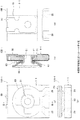
図6は本発明の第二の実施の形態にかかる電子部品用基板1−2を示す図であり、図6(a)は平面図、図6(b)は正面図、図6(c)は図6(a)のD−D断面図、図6(d)は裏面図である。同図に示す電子部品用基板1−2において前記電子部品用基板1−1と同一部分には同一符号を付してその詳細な説明は省略する。この電子部品用基板1−2においても、絶縁基台10の上面にフレキシブル回路基板20をインサート成形によって一体に取り付けて構成しており、またフレキシブル回路基板20上に形成される抵抗体パターン25は物理的蒸着又は化学的蒸着による金属薄膜によって構成されている。
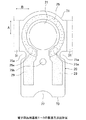
図8,図9は本発明の第三の実施の形態にかかる電子部品用基板1−3を示す図であり、図8(a)は上側から見た斜視図、図8(b)は下側から見た斜視図、図9(a)は平面図、図9(b)は正面図、図9(c)は図9(a)のE−E断面図、図9(d)は裏面図である。同図に示す電子部品用基板1−3において前記電子部品用基板1−1,1−2と同一部分には同一符号を付してその詳細な説明は省略する。この電子部品用基板1−3においても、絶縁基台10の上面にフレキシブル回路基板20をインサート成形によって一体に取り付けて構成しており、またフレキシブル回路基板20上に形成される抵抗体パターン25は物理的蒸着又は化学的蒸着による金属薄膜によって構成されている。なおこの電子部品用基板1−3を構成する各部材の材質及びその製造方法は、上記第一,第二の実施の形態の対応する各部材の材質及びその製造方法と同じである。
10 絶縁基台
11 貫通孔
15 集電板収納凹部
20 フレキシブル回路基板
21 貫通孔
25 抵抗体パターン(導体パターン)
29,29 端子パターン
31 連結部
41,45 金型
C1 キャビティー
100−1 半固定可変抵抗器
50 集電板
51 筒状突起
60 摺動子
61 嵌挿孔
63 摺動接点
1−2 電子部品用基板
50−2 集電板
51−2 筒状突起
53−2 基部
55−2 接続部
100−2 半固定可変抵抗器
1−3 電子部品用基板
17a,17b,17c 押え部
50−3 集電板
51−3 筒状突起
53−3 基部
55−3 接続部
71 端辺
73 端辺
75a,75b 樹脂挿通部
Claims (7)
- 絶縁基台と、
前記絶縁基台上に取り付けられる合成樹脂フイルム上に端子パターンとその表面に摺動子が摺接する導体パターンとを設けてなるフレキシブル回路基板とを具備し、
前記導体パターンを、物理的蒸着又は化学的蒸着による金属薄膜によって構成したことを特徴とする電子部品用基板。 - 前記金属薄膜は、ニッケル系又はサーメット系又はタンタル系の材料で構成されていることを特徴とする請求項1に記載の電子部品用基板。
- 前記絶縁基台は合成樹脂成形品であり、前記フレキシブル回路基板はこの絶縁基台にインサート成形されていることを特徴とする請求項1又は2に記載の電子部品用基板。
- 前記絶縁基台には、筒状突起を設けた集電板が、筒状突起が前記絶縁基台とフレキシブル回路基板にそれぞれ設けた貫通孔の中に位置するように、インサート成形されていることを特徴とする請求項3に記載の電子部品用基板。
- 合成樹脂成形品からなる絶縁基台と、
合成樹脂フイルム上に端子パターンとその表面に摺動子が摺接する導体パターンとを設けてなるフレキシブル回路基板とを具備し、
前記フレキシブル回路基板は、前記絶縁基台の上面と下面にその表面が露出するように折り曲げられた状態でインサート成形によって絶縁基台に取り付けられ、
さらに前記絶縁基台には、フレキシブル回路基板を前記絶縁基台に強固に固定する押え部を設けたことを特徴とする電子部品用基板。 - 前記フレキシブル回路基板の導体パターンを設けた部分は絶縁基台の上面に設置され、一方端子パターンを設けた部分は絶縁基台の上面から外周側面を介して下面に折り曲げられて設置され、
少なくとも前記絶縁基台の下面に折り曲げられた前記フレキシブル回路基板の端子パターンを設けた側の端辺に前記押え部が設けられていることを特徴とする請求項5に記載の電子部品用基板。 - 前記導体パターンを、物理的蒸着又は化学的蒸着による金属薄膜によって構成したことを特徴とする請求項5又は6に記載の電子部品用基板。
Priority Applications (6)
| Application Number | Priority Date | Filing Date | Title |
|---|---|---|---|
| JP2003409463A JP4371794B2 (ja) | 2003-02-12 | 2003-12-08 | 電子部品用基板 |
| PCT/JP2004/001199 WO2004072993A1 (ja) | 2003-02-12 | 2004-02-05 | 電子部品用基板及びその製造方法 |
| US10/541,459 US7728710B2 (en) | 2003-02-12 | 2004-02-05 | Electronic parts board and method of producing the same |
| DE112004000260T DE112004000260T5 (de) | 2003-02-12 | 2004-02-05 | Elektronikbauteilleiterplatte und Verfahren zu deren Herstellung |
| KR1020057014239A KR20050103913A (ko) | 2003-02-12 | 2004-02-05 | 전자부품용 보드 및 그 제조방법 |
| TW093103295A TWI252495B (en) | 2003-02-12 | 2004-02-12 | Substrate for electronic component and method of producing the same |
Applications Claiming Priority (2)
| Application Number | Priority Date | Filing Date | Title |
|---|---|---|---|
| JP2003034180 | 2003-02-12 | ||
| JP2003409463A JP4371794B2 (ja) | 2003-02-12 | 2003-12-08 | 電子部品用基板 |
Publications (2)
| Publication Number | Publication Date |
|---|---|
| JP2004266253A true JP2004266253A (ja) | 2004-09-24 |
| JP4371794B2 JP4371794B2 (ja) | 2009-11-25 |
Family
ID=33133900
Family Applications (1)
| Application Number | Title | Priority Date | Filing Date |
|---|---|---|---|
| JP2003409463A Expired - Fee Related JP4371794B2 (ja) | 2003-02-12 | 2003-12-08 | 電子部品用基板 |
Country Status (1)
| Country | Link |
|---|---|
| JP (1) | JP4371794B2 (ja) |
Cited By (3)
| Publication number | Priority date | Publication date | Assignee | Title |
|---|---|---|---|---|
| JP2006319141A (ja) * | 2005-05-12 | 2006-11-24 | Teikoku Tsushin Kogyo Co Ltd | 回転式電子部品 |
| JPWO2007043223A1 (ja) * | 2005-10-07 | 2009-04-16 | 株式会社村田製作所 | 可変抵抗器 |
| CN111627625A (zh) * | 2020-05-22 | 2020-09-04 | 孙文 | 一种贴片电阻 |
Families Citing this family (2)
| Publication number | Priority date | Publication date | Assignee | Title |
|---|---|---|---|---|
| US8794303B2 (en) | 2007-07-23 | 2014-08-05 | Tokyo Roki Co., Ltd. | Plate laminate type heat exchanger |
| CN101874192B (zh) | 2007-07-23 | 2012-04-18 | 东京滤器株式会社 | 板层积式热交换器 |
-
2003
- 2003-12-08 JP JP2003409463A patent/JP4371794B2/ja not_active Expired - Fee Related
Cited By (4)
| Publication number | Priority date | Publication date | Assignee | Title |
|---|---|---|---|---|
| JP2006319141A (ja) * | 2005-05-12 | 2006-11-24 | Teikoku Tsushin Kogyo Co Ltd | 回転式電子部品 |
| JPWO2007043223A1 (ja) * | 2005-10-07 | 2009-04-16 | 株式会社村田製作所 | 可変抵抗器 |
| CN111627625A (zh) * | 2020-05-22 | 2020-09-04 | 孙文 | 一种贴片电阻 |
| CN111627625B (zh) * | 2020-05-22 | 2021-12-31 | 深圳市慧达云泰科技有限公司 | 一种贴片电阻 |
Also Published As
| Publication number | Publication date |
|---|---|
| JP4371794B2 (ja) | 2009-11-25 |
Similar Documents
| Publication | Publication Date | Title |
|---|---|---|
| US7728710B2 (en) | Electronic parts board and method of producing the same | |
| JPH02220314A (ja) | フレキシブル基板内蔵の電子部品樹脂モールドケース及びその製造方法 | |
| JP4371794B2 (ja) | 電子部品用基板 | |
| JP2004266255A (ja) | 電子部品用基板の製造方法 | |
| JPH08153608A (ja) | 可変抵抗器 | |
| JP2004266256A (ja) | 電子部品用基板 | |
| JP4360989B2 (ja) | 回転式電子部品用基板及び回転式電子部品用基板の製造方法 | |
| JP2004266257A (ja) | 電子部品用基板の製造方法 | |
| JP3868796B2 (ja) | 電気部品 | |
| JP2003124009A (ja) | 可変抵抗器 | |
| JPH09213503A (ja) | 抵抗器及びその作製方法 | |
| CN110896009B (zh) | 带电阻器的电刷式开关及其制造方法 | |
| JP2531012B2 (ja) | 可変抵抗器 | |
| JPH055361B2 (ja) | ||
| JP2006049523A (ja) | 面実装用電子部品 | |
| JPH1126214A (ja) | 可変抵抗器 | |
| JP2006049522A (ja) | 回転式電子部品及びその実装基板への取付構造及び回転式電子部品の製造方法 | |
| JP3704418B2 (ja) | スライド形可変抵抗器 | |
| JPS6127843B2 (ja) | ||
| JP2006344818A (ja) | 電子部品用基体及びその製造方法 | |
| JPH0570286B2 (ja) | ||
| JPS62190703A (ja) | 可変抵抗器用抵抗基体の製造方法 | |
| JPH11162719A (ja) | チップ抵抗器とその製造方法 | |
| JPS6246048B2 (ja) | ||
| JP2006073989A (ja) | 回転式電子部品の実装基板への取付構造 |
Legal Events
| Date | Code | Title | Description |
|---|---|---|---|
| A521 | Written amendment |
Free format text: JAPANESE INTERMEDIATE CODE: A821 Effective date: 20060410 |
|
| A621 | Written request for application examination |
Free format text: JAPANESE INTERMEDIATE CODE: A621 Effective date: 20060410 |
|
| A131 | Notification of reasons for refusal |
Free format text: JAPANESE INTERMEDIATE CODE: A131 Effective date: 20090106 |
|
| A521 | Written amendment |
Free format text: JAPANESE INTERMEDIATE CODE: A821 Effective date: 20090304 Free format text: JAPANESE INTERMEDIATE CODE: A523 Effective date: 20090304 |
|
| TRDD | Decision of grant or rejection written | ||
| A01 | Written decision to grant a patent or to grant a registration (utility model) |
Free format text: JAPANESE INTERMEDIATE CODE: A01 Effective date: 20090901 |
|
| A01 | Written decision to grant a patent or to grant a registration (utility model) |
Free format text: JAPANESE INTERMEDIATE CODE: A01 |
|
| A61 | First payment of annual fees (during grant procedure) |
Free format text: JAPANESE INTERMEDIATE CODE: A61 Effective date: 20090901 |
|
| FPAY | Renewal fee payment (prs date is renewal date of database) |
Free format text: PAYMENT UNTIL: 20120911 Year of fee payment: 3 |
|
| R150 | Certificate of patent (=grant) or registration of utility model |
Free format text: JAPANESE INTERMEDIATE CODE: R150 |
|
| FPAY | Renewal fee payment (prs date is renewal date of database) |
Free format text: PAYMENT UNTIL: 20130911 Year of fee payment: 4 |
|
| LAPS | Cancellation because of no payment of annual fees |