JP2004349676A - 半導体素子の製造方法 - Google Patents
半導体素子の製造方法 Download PDFInfo
- Publication number
- JP2004349676A JP2004349676A JP2003383104A JP2003383104A JP2004349676A JP 2004349676 A JP2004349676 A JP 2004349676A JP 2003383104 A JP2003383104 A JP 2003383104A JP 2003383104 A JP2003383104 A JP 2003383104A JP 2004349676 A JP2004349676 A JP 2004349676A
- Authority
- JP
- Japan
- Prior art keywords
- contact
- semiconductor substrate
- temperature
- manufacturing
- semiconductor device
- Prior art date
- Legal status (The legal status is an assumption and is not a legal conclusion. Google has not performed a legal analysis and makes no representation as to the accuracy of the status listed.)
- Granted
Links
Images


Classifications
-
- H—ELECTRICITY
- H10—SEMICONDUCTOR DEVICES; ELECTRIC SOLID-STATE DEVICES NOT OTHERWISE PROVIDED FOR
- H10D—INORGANIC ELECTRIC SEMICONDUCTOR DEVICES
- H10D64/00—Electrodes of devices having potential barriers
- H10D64/01—Manufacture or treatment
- H10D64/011—Manufacture or treatment of electrodes ohmically coupled to a semiconductor
-
- H—ELECTRICITY
- H10—SEMICONDUCTOR DEVICES; ELECTRIC SOLID-STATE DEVICES NOT OTHERWISE PROVIDED FOR
- H10P—GENERIC PROCESSES OR APPARATUS FOR THE MANUFACTURE OR TREATMENT OF DEVICES COVERED BY CLASS H10
- H10P95/00—Generic processes or apparatus for manufacture or treatments not covered by the other groups of this subclass
- H10P95/90—Thermal treatments, e.g. annealing or sintering
-
- H—ELECTRICITY
- H10—SEMICONDUCTOR DEVICES; ELECTRIC SOLID-STATE DEVICES NOT OTHERWISE PROVIDED FOR
- H10D—INORGANIC ELECTRIC SEMICONDUCTOR DEVICES
- H10D64/00—Electrodes of devices having potential barriers
- H10D64/01—Manufacture or treatment
- H10D64/011—Manufacture or treatment of electrodes ohmically coupled to a semiconductor
- H10D64/0111—Manufacture or treatment of electrodes ohmically coupled to a semiconductor to Group IV semiconductors
-
- H—ELECTRICITY
- H10—SEMICONDUCTOR DEVICES; ELECTRIC SOLID-STATE DEVICES NOT OTHERWISE PROVIDED FOR
- H10P—GENERIC PROCESSES OR APPARATUS FOR THE MANUFACTURE OR TREATMENT OF DEVICES COVERED BY CLASS H10
- H10P32/00—Diffusion of dopants within, into or out of wafers, substrates or parts of devices
- H10P32/10—Diffusion of dopants within, into or out of semiconductor bodies or layers
- H10P32/12—Diffusion of dopants within, into or out of semiconductor bodies or layers between a solid phase and a gaseous phase
- H10P32/1204—Diffusion of dopants within, into or out of semiconductor bodies or layers between a solid phase and a gaseous phase from a plasma phase
-
- H—ELECTRICITY
- H10—SEMICONDUCTOR DEVICES; ELECTRIC SOLID-STATE DEVICES NOT OTHERWISE PROVIDED FOR
- H10P—GENERIC PROCESSES OR APPARATUS FOR THE MANUFACTURE OR TREATMENT OF DEVICES COVERED BY CLASS H10
- H10P70/00—Cleaning of wafers, substrates or parts of devices
- H10P70/20—Cleaning during device manufacture
- H10P70/23—Cleaning during device manufacture during, before or after processing of insulating materials
- H10P70/234—Cleaning during device manufacture during, before or after processing of insulating materials the processing being the formation of vias or contact holes
-
- H—ELECTRICITY
- H10—SEMICONDUCTOR DEVICES; ELECTRIC SOLID-STATE DEVICES NOT OTHERWISE PROVIDED FOR
- H10W—GENERIC PACKAGES, INTERCONNECTIONS, CONNECTORS OR OTHER CONSTRUCTIONAL DETAILS OF DEVICES COVERED BY CLASS H10
- H10W20/00—Interconnections in chips, wafers or substrates
- H10W20/01—Manufacture or treatment
- H10W20/071—Manufacture or treatment of dielectric parts thereof
- H10W20/081—Manufacture or treatment of dielectric parts thereof by forming openings in the dielectric parts
-
- H—ELECTRICITY
- H10—SEMICONDUCTOR DEVICES; ELECTRIC SOLID-STATE DEVICES NOT OTHERWISE PROVIDED FOR
- H10W—GENERIC PACKAGES, INTERCONNECTIONS, CONNECTORS OR OTHER CONSTRUCTIONAL DETAILS OF DEVICES COVERED BY CLASS H10
- H10W20/00—Interconnections in chips, wafers or substrates
- H10W20/01—Manufacture or treatment
- H10W20/071—Manufacture or treatment of dielectric parts thereof
- H10W20/093—Manufacture or treatment of dielectric parts thereof by modifying materials of the dielectric parts
- H10W20/096—Manufacture or treatment of dielectric parts thereof by modifying materials of the dielectric parts by contacting with gases, liquids or plasmas
-
- H—ELECTRICITY
- H10—SEMICONDUCTOR DEVICES; ELECTRIC SOLID-STATE DEVICES NOT OTHERWISE PROVIDED FOR
- H10W—GENERIC PACKAGES, INTERCONNECTIONS, CONNECTORS OR OTHER CONSTRUCTIONAL DETAILS OF DEVICES COVERED BY CLASS H10
- H10W20/00—Interconnections in chips, wafers or substrates
- H10W20/01—Manufacture or treatment
- H10W20/071—Manufacture or treatment of dielectric parts thereof
- H10W20/093—Manufacture or treatment of dielectric parts thereof by modifying materials of the dielectric parts
- H10W20/097—Manufacture or treatment of dielectric parts thereof by modifying materials of the dielectric parts by thermally treating
Landscapes
- Internal Circuitry In Semiconductor Integrated Circuit Devices (AREA)
- Electrodes Of Semiconductors (AREA)
Abstract
【解決手段】接合領域42を含んだ所定の下部構造物が形成された半導体基板41を用意する段階と、前記半導体基板の上面全面に層間絶縁膜43を形成する段階と、前記層間絶縁膜をエッチングして接合領域を露出させるコンタクトホール45を形成する段階と、前記コンタクトホールにより露出された半導体基板の表面に対し順次に乾式及び湿式洗浄する段階と、前記洗浄された半導体基板のコンタクト表面を還元性ガス雰囲気で前処理してコンタクト表面に形成された自然酸化膜を除去する段階と、前記前処理されたコンタクト表面での不純物損失が補償されるようにイン−シトウ(in−situ)で接合領域の表面に不純物を追加ドーピングする段階と、前記コンタクトホール及び層間絶縁膜上にイン−シトウで導電膜46を蒸着する段階とを含む。
【選択図】図9
Description
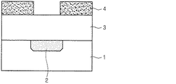
図1乃至図3は従来技術による半導体素子の製造方法を説明するための工程別断面図である。
したがって、このような自然酸化膜を除去するために本発明では、基板の結果物を装置内に装入させた後、まず、水素またはアンモニアガスのような還元性ガス、望ましくは、水素ガス雰囲気で前処理を行なう。
42 接合領域
43 層間絶縁膜
45 コンタクトホール
46 金属配線
Claims (6)
- 接合領域を含んだ所定の下部構造物が形成された半導体基板を用意する段階と、
前記半導体基板の上面全面に層間絶縁膜を形成する段階と、
前記層間絶縁膜をエッチングして接合領域を露出させるコンタクトホールを形成する段階と、
前記コンタクトホールにより露出された半導体基板の表面に対し順次に乾式及び湿式洗浄する段階と、
前記洗浄された半導体基板のコンタクト表面を還元性ガス雰囲気で前処理してコンタクト表面に形成された自然酸化膜を除去する段階と、
前記前処理されたコンタクト表面での不純物損失が補償されるようにイン−シトウ(in−situ)で接合領域の表面に不純物を追加ドーピングする段階と、
前記コンタクトホール及び層間絶縁膜上にイン−シトウで導電膜を蒸着する段階とを含むこと特徴とする半導体素子の製造方法。 - 前記還元性ガスは、水素ガスまたはアンモニアガスを含むことを特徴とする請求項1に記載の半導体素子の製造方法。
- 前記還元性ガス雰囲気での前処理は、低温プラズマ処理または高温熱処理で遂行することを特徴とする請求項1に記載の半導体素子の製造方法。
- 前記低温プラズマ処理は、水素ガスを1〜1000sccm(standard cc/min)の流量で流しながら、1〜300Torrの圧力、及び常温〜600℃の温度下で遂行することを特徴とする請求項3に記載の半導体素子の製造方法。
- 前記高温熱処理は、水素ガスを1〜5slm(standard liter/min)の流量で流しながら、1〜300Torrの圧力、及び700〜1000℃の温度下で遂行することを特徴とする請求項3に記載の半導体素子の製造方法。
- 前記コンタクト表面に不純物を追加ドーピングする段階は、損失された不純物を内包する物質を装置内に供給した後、低温プラズマ処理または高温熱処理することにより遂行されることを特徴とする請求項1に記載の半導体素子の製造方法。
Applications Claiming Priority (1)
| Application Number | Priority Date | Filing Date | Title |
|---|---|---|---|
| KR10-2003-0032210A KR100518228B1 (ko) | 2003-05-21 | 2003-05-21 | 반도체 소자의 제조방법 |
Publications (2)
| Publication Number | Publication Date |
|---|---|
| JP2004349676A true JP2004349676A (ja) | 2004-12-09 |
| JP4508607B2 JP4508607B2 (ja) | 2010-07-21 |
Family
ID=36592766
Family Applications (1)
| Application Number | Title | Priority Date | Filing Date |
|---|---|---|---|
| JP2003383104A Expired - Fee Related JP4508607B2 (ja) | 2003-05-21 | 2003-11-12 | 半導体素子の製造方法 |
Country Status (5)
| Country | Link |
|---|---|
| US (1) | US6979633B2 (ja) |
| JP (1) | JP4508607B2 (ja) |
| KR (1) | KR100518228B1 (ja) |
| CN (1) | CN1282999C (ja) |
| TW (1) | TWI234203B (ja) |
Families Citing this family (17)
| Publication number | Priority date | Publication date | Assignee | Title |
|---|---|---|---|---|
| CN101593678B (zh) * | 2008-05-30 | 2012-05-16 | 中芯国际集成电路制造(北京)有限公司 | 掺杂区形成方法 |
| CN101969048B (zh) * | 2009-07-27 | 2012-07-25 | 中芯国际集成电路制造(上海)有限公司 | 存储器件的制作方法 |
| CN101724896B (zh) * | 2009-11-26 | 2012-08-08 | 上海宏力半导体制造有限公司 | 一种非选择性生长锗硅外延的方法 |
| KR101062862B1 (ko) * | 2010-07-07 | 2011-09-07 | 주식회사 하이닉스반도체 | 측벽접합을 구비한 반도체장치 제조 방법 |
| CN103346126A (zh) * | 2013-06-26 | 2013-10-09 | 上海宏力半导体制造有限公司 | 闪存存储单元的形成方法 |
| US20150093889A1 (en) * | 2013-10-02 | 2015-04-02 | Intermolecular | Methods for removing a native oxide layer from germanium susbtrates in the fabrication of integrated circuits |
| CN104091762A (zh) * | 2014-07-16 | 2014-10-08 | 上海先进半导体制造股份有限公司 | 双极型晶体管的制备方法 |
| CN108538780A (zh) * | 2018-04-18 | 2018-09-14 | 睿力集成电路有限公司 | 位线/存储节点接触栓塞和多晶硅接触薄膜的制造方法 |
| CN110911265A (zh) * | 2018-09-17 | 2020-03-24 | 长鑫存储技术有限公司 | 在氮化钛生成工艺中去除氧化硅的方法 |
| US11088147B2 (en) | 2019-06-26 | 2021-08-10 | Micron Technology, Inc. | Apparatus with doped surfaces, and related methods with in situ doping |
| CN111446156A (zh) * | 2020-04-03 | 2020-07-24 | 合肥晶合集成电路有限公司 | 半导体结构的形成方法及半导体结构 |
| CN114063320B (zh) * | 2020-07-31 | 2024-09-17 | 中芯国际集成电路制造(上海)有限公司 | 半导体结构及其形成方法 |
| US12278142B2 (en) | 2022-05-11 | 2025-04-15 | Nanya Technology Corporation | Method for manfacturing semiconductor device for reducing partcle-induced defects |
| TWI826174B (zh) * | 2022-05-11 | 2023-12-11 | 南亞科技股份有限公司 | 半導體元件的製備方法 |
| US12211739B2 (en) | 2022-05-11 | 2025-01-28 | Nanya Technology Corporation | Method for manufacturing semiconductor device comprising contact void surrounding bit line |
| CN115458409A (zh) * | 2022-08-25 | 2022-12-09 | 上海华力集成电路制造有限公司 | 一种SiGe沟道的形成方法 |
| US20240331999A1 (en) * | 2023-03-31 | 2024-10-03 | Applied Materials, Inc. | Systems and methods for nanohole wet cleans |
Citations (5)
| Publication number | Priority date | Publication date | Assignee | Title |
|---|---|---|---|---|
| JPH0669152A (ja) * | 1992-08-20 | 1994-03-11 | Matsushita Electron Corp | 半導体装置およびその製造方法 |
| JPH11204455A (ja) * | 1998-01-13 | 1999-07-30 | Sony Corp | 半導体装置の製造方法 |
| JP2003115462A (ja) * | 2001-10-05 | 2003-04-18 | Kawasaki Microelectronics Kk | コンタクト構造の形成方法 |
| JP2003124140A (ja) * | 2001-10-12 | 2003-04-25 | Hynix Semiconductor Inc | 半導体素子の製造方法 |
| JP2003124314A (ja) * | 2001-10-08 | 2003-04-25 | Hynix Semiconductor Inc | 半導体素子の製造方法 |
Family Cites Families (4)
| Publication number | Priority date | Publication date | Assignee | Title |
|---|---|---|---|---|
| JPH0618236B2 (ja) | 1987-07-01 | 1994-03-09 | 富士電機株式会社 | 半導体素子の製造方法 |
| JP2978748B2 (ja) | 1995-11-22 | 1999-11-15 | 日本電気株式会社 | 半導体装置の製造方法 |
| JP4663038B2 (ja) * | 1997-05-28 | 2011-03-30 | 三菱電機株式会社 | コンタクトホールの形成方法 |
| US6242331B1 (en) * | 1999-12-20 | 2001-06-05 | Taiwan Semiconductor Manufacturing Company | Method to reduce device contact resistance using a hydrogen peroxide treatment |
-
2003
- 2003-05-21 KR KR10-2003-0032210A patent/KR100518228B1/ko not_active Expired - Fee Related
- 2003-11-07 US US10/704,231 patent/US6979633B2/en not_active Expired - Fee Related
- 2003-11-07 TW TW092131157A patent/TWI234203B/zh not_active IP Right Cessation
- 2003-11-12 JP JP2003383104A patent/JP4508607B2/ja not_active Expired - Fee Related
- 2003-11-25 CN CNB2003101181947A patent/CN1282999C/zh not_active Expired - Fee Related
Patent Citations (5)
| Publication number | Priority date | Publication date | Assignee | Title |
|---|---|---|---|---|
| JPH0669152A (ja) * | 1992-08-20 | 1994-03-11 | Matsushita Electron Corp | 半導体装置およびその製造方法 |
| JPH11204455A (ja) * | 1998-01-13 | 1999-07-30 | Sony Corp | 半導体装置の製造方法 |
| JP2003115462A (ja) * | 2001-10-05 | 2003-04-18 | Kawasaki Microelectronics Kk | コンタクト構造の形成方法 |
| JP2003124314A (ja) * | 2001-10-08 | 2003-04-25 | Hynix Semiconductor Inc | 半導体素子の製造方法 |
| JP2003124140A (ja) * | 2001-10-12 | 2003-04-25 | Hynix Semiconductor Inc | 半導体素子の製造方法 |
Also Published As
| Publication number | Publication date |
|---|---|
| TW200426942A (en) | 2004-12-01 |
| JP4508607B2 (ja) | 2010-07-21 |
| TWI234203B (en) | 2005-06-11 |
| KR100518228B1 (ko) | 2005-10-04 |
| CN1282999C (zh) | 2006-11-01 |
| CN1574290A (zh) | 2005-02-02 |
| US20040235282A1 (en) | 2004-11-25 |
| US6979633B2 (en) | 2005-12-27 |
| KR20040100015A (ko) | 2004-12-02 |
Similar Documents
| Publication | Publication Date | Title |
|---|---|---|
| JP4508607B2 (ja) | 半導体素子の製造方法 | |
| JPH06140372A (ja) | 半導体装置の製造方法 | |
| US20230420295A1 (en) | Treatment of tungsten surface for tungsten gap-fill | |
| KR20020083770A (ko) | 반도체 소자의 콘택 플러그 형성방법 | |
| US6444518B2 (en) | Method and manufacturing a device separation film in a semiconductor device | |
| JPH08306781A (ja) | 半導体装置の製造方法 | |
| JP4798688B2 (ja) | 半導体装置の製造方法 | |
| US7125809B1 (en) | Method and material for removing etch residue from high aspect ratio contact surfaces | |
| JP2000058643A (ja) | プラグの形成方法 | |
| US20070087573A1 (en) | Pre-treatment method for physical vapor deposition of metal layer and method of forming metal silicide layer | |
| JP2008305921A (ja) | 半導体装置及びその製造方法 | |
| US20070045227A1 (en) | Method of stripping photoresist | |
| JPH02139932A (ja) | 半導体装置の製造方法 | |
| CN104465518A (zh) | 栅极制作方法 | |
| KR100273716B1 (ko) | 반도체 소자의 제조방법 | |
| CN114068399B (zh) | 半导体结构的形成方法 | |
| JP3550632B2 (ja) | 半導体装置 | |
| TWI489551B (zh) | 製造具有微小圖案之半導體元件的方法 | |
| KR100372655B1 (ko) | 반도체소자의도선층형성방법 | |
| JPH1187272A (ja) | 半導体装置の製造方法 | |
| KR100197652B1 (ko) | 반도체소자의 도전배선 형성방법 | |
| KR100687876B1 (ko) | 반도체 소자의 금속 콘택 형성 방법 | |
| KR20060011396A (ko) | 반도체 소자의 다층 금속배선 형성방법 | |
| JP2004039879A (ja) | 半導体装置の製造方法 | |
| US6472270B1 (en) | Elimination of voids at the oxide/silicon interface in trench-based structures |
Legal Events
| Date | Code | Title | Description |
|---|---|---|---|
| A621 | Written request for application examination |
Free format text: JAPANESE INTERMEDIATE CODE: A621 Effective date: 20060912 |
|
| A977 | Report on retrieval |
Free format text: JAPANESE INTERMEDIATE CODE: A971007 Effective date: 20090820 |
|
| A131 | Notification of reasons for refusal |
Free format text: JAPANESE INTERMEDIATE CODE: A131 Effective date: 20090825 |
|
| A521 | Request for written amendment filed |
Free format text: JAPANESE INTERMEDIATE CODE: A523 Effective date: 20091125 |
|
| A131 | Notification of reasons for refusal |
Free format text: JAPANESE INTERMEDIATE CODE: A131 Effective date: 20091222 |
|
| A521 | Request for written amendment filed |
Free format text: JAPANESE INTERMEDIATE CODE: A523 Effective date: 20100317 |
|
| TRDD | Decision of grant or rejection written | ||
| A01 | Written decision to grant a patent or to grant a registration (utility model) |
Free format text: JAPANESE INTERMEDIATE CODE: A01 Effective date: 20100406 |
|
| A01 | Written decision to grant a patent or to grant a registration (utility model) |
Free format text: JAPANESE INTERMEDIATE CODE: A01 |
|
| A61 | First payment of annual fees (during grant procedure) |
Free format text: JAPANESE INTERMEDIATE CODE: A61 Effective date: 20100427 |
|
| FPAY | Renewal fee payment (event date is renewal date of database) |
Free format text: PAYMENT UNTIL: 20130514 Year of fee payment: 3 |
|
| R150 | Certificate of patent or registration of utility model |
Free format text: JAPANESE INTERMEDIATE CODE: R150 |
|
| LAPS | Cancellation because of no payment of annual fees |