JP2004361402A - X-ray and CT image detector - Google Patents
X-ray and CT image detector Download PDFInfo
- Publication number
- JP2004361402A JP2004361402A JP2004162780A JP2004162780A JP2004361402A JP 2004361402 A JP2004361402 A JP 2004361402A JP 2004162780 A JP2004162780 A JP 2004162780A JP 2004162780 A JP2004162780 A JP 2004162780A JP 2004361402 A JP2004361402 A JP 2004361402A
- Authority
- JP
- Japan
- Prior art keywords
- layer
- photoreceptor
- backing layer
- ray detector
- connection point
- Prior art date
- Legal status (The legal status is an assumption and is not a legal conclusion. Google has not performed a legal analysis and makes no representation as to the accuracy of the status listed.)
- Granted
Links
- 239000010410 layer Substances 0.000 claims abstract description 225
- 108091008695 photoreceptors Proteins 0.000 claims abstract description 55
- 239000011521 glass Substances 0.000 claims abstract description 34
- 239000011229 interlayer Substances 0.000 claims abstract description 16
- 238000000034 method Methods 0.000 claims description 20
- 239000000919 ceramic Substances 0.000 claims description 18
- 238000004519 manufacturing process Methods 0.000 claims description 4
- 239000004020 conductor Substances 0.000 claims description 2
- 238000002591 computed tomography Methods 0.000 abstract description 16
- 238000003325 tomography Methods 0.000 abstract description 3
- 230000008569 process Effects 0.000 description 11
- 238000003384 imaging method Methods 0.000 description 10
- 229920000642 polymer Polymers 0.000 description 10
- 239000000758 substrate Substances 0.000 description 6
- XUIMIQQOPSSXEZ-UHFFFAOYSA-N Silicon Chemical compound [Si] XUIMIQQOPSSXEZ-UHFFFAOYSA-N 0.000 description 5
- 238000005229 chemical vapour deposition Methods 0.000 description 5
- 239000013078 crystal Substances 0.000 description 5
- 239000011159 matrix material Substances 0.000 description 5
- 229920001721 polyimide Polymers 0.000 description 5
- 229910052710 silicon Inorganic materials 0.000 description 5
- 239000010703 silicon Substances 0.000 description 5
- 239000004642 Polyimide Substances 0.000 description 4
- 230000008901 benefit Effects 0.000 description 4
- 239000000463 material Substances 0.000 description 4
- 229910052751 metal Inorganic materials 0.000 description 4
- 239000002184 metal Substances 0.000 description 4
- 229920000307 polymer substrate Polymers 0.000 description 4
- WFKWXMTUELFFGS-UHFFFAOYSA-N tungsten Chemical compound [W] WFKWXMTUELFFGS-UHFFFAOYSA-N 0.000 description 4
- 229910052721 tungsten Inorganic materials 0.000 description 4
- 239000010937 tungsten Substances 0.000 description 4
- 239000004593 Epoxy Substances 0.000 description 3
- 229910052782 aluminium Inorganic materials 0.000 description 3
- XAGFODPZIPBFFR-UHFFFAOYSA-N aluminium Chemical compound [Al] XAGFODPZIPBFFR-UHFFFAOYSA-N 0.000 description 3
- 229910021417 amorphous silicon Inorganic materials 0.000 description 3
- 238000005452 bending Methods 0.000 description 3
- 238000013170 computed tomography imaging Methods 0.000 description 3
- 230000003287 optical effect Effects 0.000 description 3
- RYGMFSIKBFXOCR-UHFFFAOYSA-N Copper Chemical compound [Cu] RYGMFSIKBFXOCR-UHFFFAOYSA-N 0.000 description 2
- XEEYBQQBJWHFJM-UHFFFAOYSA-N Iron Chemical compound [Fe] XEEYBQQBJWHFJM-UHFFFAOYSA-N 0.000 description 2
- GWEVSGVZZGPLCZ-UHFFFAOYSA-N Titan oxide Chemical compound O=[Ti]=O GWEVSGVZZGPLCZ-UHFFFAOYSA-N 0.000 description 2
- 229910010293 ceramic material Inorganic materials 0.000 description 2
- 239000011248 coating agent Substances 0.000 description 2
- 238000000576 coating method Methods 0.000 description 2
- 229910052802 copper Inorganic materials 0.000 description 2
- 239000010949 copper Substances 0.000 description 2
- 239000011888 foil Substances 0.000 description 2
- 230000000873 masking effect Effects 0.000 description 2
- 230000002093 peripheral effect Effects 0.000 description 2
- 238000002360 preparation method Methods 0.000 description 2
- 230000005855 radiation Effects 0.000 description 2
- 229910052716 thallium Inorganic materials 0.000 description 2
- BKVIYDNLLOSFOA-UHFFFAOYSA-N thallium Chemical compound [Tl] BKVIYDNLLOSFOA-UHFFFAOYSA-N 0.000 description 2
- 229920002799 BoPET Polymers 0.000 description 1
- OKTJSMMVPCPJKN-UHFFFAOYSA-N Carbon Chemical compound [C] OKTJSMMVPCPJKN-UHFFFAOYSA-N 0.000 description 1
- 239000005041 Mylar™ Substances 0.000 description 1
- 239000000853 adhesive Substances 0.000 description 1
- 230000001070 adhesive effect Effects 0.000 description 1
- 239000000956 alloy Substances 0.000 description 1
- 229910045601 alloy Inorganic materials 0.000 description 1
- 230000002238 attenuated effect Effects 0.000 description 1
- 230000015556 catabolic process Effects 0.000 description 1
- 238000012937 correction Methods 0.000 description 1
- 238000005336 cracking Methods 0.000 description 1
- 238000006731 degradation reaction Methods 0.000 description 1
- 230000032798 delamination Effects 0.000 description 1
- 238000005137 deposition process Methods 0.000 description 1
- 238000002059 diagnostic imaging Methods 0.000 description 1
- 238000005553 drilling Methods 0.000 description 1
- 230000008030 elimination Effects 0.000 description 1
- 238000003379 elimination reaction Methods 0.000 description 1
- 230000005669 field effect Effects 0.000 description 1
- 239000012467 final product Substances 0.000 description 1
- 229910002804 graphite Inorganic materials 0.000 description 1
- 239000010439 graphite Substances 0.000 description 1
- 238000003702 image correction Methods 0.000 description 1
- 229910052742 iron Inorganic materials 0.000 description 1
- 230000031700 light absorption Effects 0.000 description 1
- 230000007246 mechanism Effects 0.000 description 1
- 238000001465 metallisation Methods 0.000 description 1
- 238000007747 plating Methods 0.000 description 1
- 238000003908 quality control method Methods 0.000 description 1
- 239000002994 raw material Substances 0.000 description 1
- 230000009467 reduction Effects 0.000 description 1
- 230000002787 reinforcement Effects 0.000 description 1
- 238000007789 sealing Methods 0.000 description 1
- 238000007493 shaping process Methods 0.000 description 1
- 229910052709 silver Inorganic materials 0.000 description 1
- 239000004332 silver Substances 0.000 description 1
- 238000005476 soldering Methods 0.000 description 1
- 239000003351 stiffener Substances 0.000 description 1
- 239000004408 titanium dioxide Substances 0.000 description 1
- 230000002792 vascular Effects 0.000 description 1
Images



Classifications
-
- G—PHYSICS
- G01—MEASURING; TESTING
- G01T—MEASUREMENT OF NUCLEAR OR X-RADIATION
- G01T1/00—Measuring X-radiation, gamma radiation, corpuscular radiation, or cosmic radiation
- G01T1/16—Measuring radiation intensity
- G01T1/20—Measuring radiation intensity with scintillation detectors
- G01T1/2018—Scintillation-photodiode combinations
Landscapes
- Physics & Mathematics (AREA)
- Health & Medical Sciences (AREA)
- Life Sciences & Earth Sciences (AREA)
- General Physics & Mathematics (AREA)
- High Energy & Nuclear Physics (AREA)
- Molecular Biology (AREA)
- Spectroscopy & Molecular Physics (AREA)
- Measurement Of Radiation (AREA)
- Apparatus For Radiation Diagnosis (AREA)
- Solid State Image Pick-Up Elements (AREA)
- Transforming Light Signals Into Electric Signals (AREA)
- Light Receiving Elements (AREA)
Abstract
【課題】 X線断層撮影又はコンピュータ断層撮影システム等で使用可能な画像検出器を提供する。
【解決手段】 X線検出器(400)は、予め選択された湾曲半径(402)に基づいて湾曲したガラス層(414)と、該ガラス層上に形成された光受容体(410)と、予め選択された湾曲半径(402)に基づいて湾曲したバッキング層(404)とを含む。バッキング層(404)は、ガラス層(414)を支持する。別の実施形態において、X線検出器は、光受容体と周辺部内に層間接続点とを含み、周辺部で界接する光受容体層を含む。
【選択図】 図4PROBLEM TO BE SOLVED: To provide an image detector usable in an X-ray tomography or a computer tomography system or the like.
An X-ray detector (400) includes a glass layer (414) curved based on a preselected curvature radius (402), and a photoreceptor (410) formed on the glass layer; A backing layer (404) curved based on a preselected radius of curvature (402). The backing layer (404) supports the glass layer (414). In another embodiment, the X-ray detector includes a photoreceptor and a photoreceptor layer that includes an interlayer connection point in the periphery and borders at the periphery.
[Selection] Figure 4
Description
本発明は一般に、医用イメージング・システムの分野に関する。詳細には、本発明は、例えばX線断層撮影又はコンピュータ断層撮影システム用の画像検出器に関する。 The present invention relates generally to the field of medical imaging systems. In particular, the invention relates to an image detector for X-ray tomography or computed tomography systems, for example.
X線システムは、2次元の平面画像を作成し、一方、コンピュータ断層撮影(CT)システムは、「スライス」又は「断層」画像とも呼ばれる2次元の断面画像を作成する。X線システム、特に血管イメージングに用いられるものにおいてCT様式の画像を得ることに対しての関心があるが、2つの形式のシステムに用いられる検出器は、かなり異なっている。その結果、以下に述べる理由により、X線検出器はCTイメージングに好適でなく、またCT検出器はX線イメージングに適合しない。 X-ray systems create two-dimensional planar images, while computed tomography (CT) systems create two-dimensional cross-sectional images, also called “slice” or “tomographic” images. Although there is an interest in obtaining CT-style images in X-ray systems, particularly those used for vascular imaging, the detectors used in the two types of systems are quite different. As a result, for the reasons described below, X-ray detectors are not suitable for CT imaging, and CT detectors are not compatible with X-ray imaging.
X線検出器は、イメージ増強管として実装された検出器の場合においては、一般に平坦であるか又は平坦な形状に近い。従って、X線を吸収するシンチレータ結晶群は、X線源に対して種々の距離及び角度に位置している。例証として、平坦な検出器の中央に位置する画素は、X線源により近接しており、X線ビームを真っ直ぐに受け取る。検出器の周辺部に位置する画素は、わずかに減衰したX線ビームをある角度で受け取る。イメージ増強管を用いるX線検出器は、湾曲した入力面を有するが、湾曲の向きは、最適画質に望ましい向きとは反対である。(ビーム減衰を最小限にするために構造材料の使用をできる限り少なくしながら大気圧による崩壊を防止するために、真空管の入力面は患者の方向にドーム形を呈していなければならない)。 X-ray detectors are generally flat or close to flat in the case of detectors implemented as image intensifier tubes. Accordingly, the scintillator crystal group that absorbs X-rays is located at various distances and angles with respect to the X-ray source. Illustratively, the pixel located in the center of the flat detector is closer to the x-ray source and receives the x-ray beam straight. Pixels located at the periphery of the detector receive a slightly attenuated x-ray beam at an angle. An x-ray detector using an image intensifier tube has a curved input surface, but the direction of curvature is opposite to that desired for optimal image quality. (In order to prevent collapse due to atmospheric pressure while using as little structural material as possible to minimize beam attenuation, the input surface of the tube must be dome-shaped in the direction of the patient).
一方、CT検出器は、バルク状で扱いにくい構造フレームを用いて、幾何学的形状、一般的に円弧の形状に組み立てられる。この点において、CT検出器組立体は、半径が一定の円弧に近接するよう多面多角形を用いた平坦な検出器素子の円弧状のアレイとして組み立てられた。以前は、各CT検出器素子は、検出器素子の上側及び下側のみを通して信号を検出器素子の外にルーティングしていた(この場合の上及び下は、検出器の軸方向に平方な方向を指す)。素子の数が増大するにつれて、検出器の上縁部及び下縁部に沿ってワイヤ密度が大幅に増大した。その結果、少数の検出器素子を越えてCT検出器の大きさ及び能力を拡大することが極めて困難となった。 CT detectors, on the other hand, are assembled into a geometric shape, typically a circular arc shape, using a bulky and unwieldy structural frame. In this regard, the CT detector assembly was assembled as an arcuate array of flat detector elements using polyhedral polygons so that the radius is close to a constant arc. Previously, each CT detector element routed signals out of the detector element only through the upper and lower sides of the detector element (in this case, the upper and lower are directions square to the axial direction of the detector). ). As the number of elements increased, the wire density increased significantly along the upper and lower edges of the detector. As a result, it has become extremely difficult to expand the size and capability of the CT detector beyond a small number of detector elements.
検出器の形状の差異は、照射後に適用される画像処理ステップの差異につながる。幾つかのX線システムは、例えば、これらのビデオ画像取得構成要素にアナモルフィック光学素子の形態の幾何学的補正を施す。これらの光学素子は、イメージ増強管の逆の湾曲に起因する画像の歪みを矯正する。平坦なX線検出器の場合、中央部と比較して検出器の周辺部において画質の損失がある。画質の損失は、単一の周辺画素により全て検出されるべきX線光子が、ある角度をなしてこれらがシンチレータ材料の厚さを通過することにより、2つ又はそれ以上の画素上のシンチレータ材料を通過することにより生じる。その結果、画像に対する光子の提供は、CT検出器素子がそうであるように検出器の周辺部がX線源に対して垂直に配向された場合よりもより多くの画素の上に分配される(ぼかされる)。画像補正アルゴリズムでさえも、この幾何学的問題による画質劣化を完全には補償することができない。フラットパネルX線検出器の画像データがCT画像再構成アルゴリズムと共に用いられる場合、この画質の損失は、このようにして取得されたCT画像にも存在する。従って、2つの種類のシステムに対する検出器は極めて異なっており、例えば、CTイメージングをX線システムに組み込むことを困難で煩雑なものとしている。 Differences in detector shape lead to differences in image processing steps applied after irradiation. Some X-ray systems, for example, apply geometric corrections in the form of anamorphic optics to these video image acquisition components. These optical elements correct image distortion due to the inverse curvature of the image intensifier tube. In the case of a flat X-ray detector, there is a loss of image quality at the periphery of the detector compared to the center. The loss of image quality is due to the fact that the X-ray photons that are all to be detected by a single peripheral pixel pass through the thickness of the scintillator material at an angle so that scintillator material on two or more pixels Caused by passing through As a result, the provision of photons to the image is distributed over more pixels than if the periphery of the detector was oriented perpendicular to the x-ray source as is the case with CT detector elements. (Blurred). Even image correction algorithms cannot fully compensate for image quality degradation due to this geometric problem. When flat panel X-ray detector image data is used in conjunction with a CT image reconstruction algorithm, this loss of image quality is also present in the CT image thus obtained. Thus, the detectors for the two types of systems are very different, making it difficult and cumbersome to incorporate, for example, CT imaging into an X-ray system.
従って、上に記載した困難性及びこれまで経験された他の困難性を少なくとも部分的に克服する画像検出器に対する必要性が存在する。 Accordingly, there is a need for an image detector that at least partially overcomes the difficulties described above and other difficulties previously experienced.
1つの実施形態において、X線検出器は、予め選択された湾曲半径に基づいて湾曲したガラス層と、該ガラス層上に形成された光受容体と、予め選択された湾曲半径に基づいて湾曲したバッキング層とを含む。バッキング層は、ガラス層を支持する。 In one embodiment, the X-ray detector includes a glass layer that is curved based on a preselected radius of curvature, a photoreceptor formed on the glass layer, and a curve that is curved based on a preselected radius of curvature. And a backing layer. The backing layer supports the glass layer.
別の実施形態において、X線検出器は、周辺部で界接する光受容体層を含む。該光受容体層は、光受容体と周辺部内に層間接続点とを含む。更に、X線検出器は、光受容体層を支持するバッキング層を含む。該バッキング層は、予め選択された湾曲半径に基づいて湾曲しており、ルーティング接続点を含む。層間接続点とルーティング接続点との間の電気的接続が、光受容体層とバッキング層との間の電気的接続性を確立する。 In another embodiment, the x-ray detector includes a photoreceptor layer that borders at the periphery. The photoreceptor layer includes a photoreceptor and interlayer connection points in the periphery. In addition, the x-ray detector includes a backing layer that supports the photoreceptor layer. The backing layer is curved based on a preselected radius of curvature and includes routing connection points. The electrical connection between the interlayer connection point and the routing connection point establishes the electrical connectivity between the photoreceptor layer and the backing layer.
本発明の他のシステム、方法、特徴、及び利点は、以下の図面及び詳細な説明を考察すれば、当業者には明らかとなるであろう。全てのこのような追加のシステム、方法、特徴、及び利点は、本説明に含まれ、本発明の範囲内にあり、且つ添付の特許請求の範囲により保護されることが意図される。 Other systems, methods, features, and advantages of the present invention will be apparent to those of ordinary skill in the art in view of the following drawings and detailed description. It is intended that all such additional systems, methods, features, and advantages be included in this description, be within the scope of the invention, and be protected by the accompanying claims.
図中の構成要素は、必ずしも縮尺通りではなく、X線検出器の原理を図示することに重きを置いたものである。図において、同じ参照番号は、異なる図の全体を通じて同じ部品を示す。 The components in the figure are not necessarily to scale, emphasis being placed on illustrating the principles of the X-ray detector. In the figures, like reference numerals designate like parts throughout the different views.
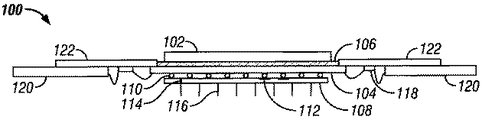
最初に図1を参照すると、CTイメージングのようなX線イメージング・システムにおける汎用用途、並びにX線イメージング・システムを備えた特定用途に好適なX線検出器100が示されている。X線検出器100は、光結合エポキシ106を介してシリコン結晶光受容体層104に取り付けられたシンチレータ層102を含む。シンチレータ層102は、タリウムドープされたCsIシンチレータ、又はイリノイ州所在のLumex of Palatineから入手可能なLumexシンチレータとすることができる。予め選択された湾曲半径に基づいて湾曲したバッキング層108は、光受容体層104を支持する。
Referring initially to FIG. 1, there is shown an
光受容体層104は、層間接続点110を含み、一方、バッキング層108は、ルーティング接続点112を含む。層間接続点110又はルーティング接続点112は、例を挙げれば、バンプ・パッド、フラット・パッド、ピン、レセプタクル、又は他の形式の信号接続性構造体とすることができる。電気的接続は、層間接続点110とルーティング接続点112との間の接触、はんだ付け、又は機械的接続により生じる。電気的接続は、これにより光受容体層104とバッキング層108との間に電気的接続性を確立する。バッキング層108内のバイア114は、光受容体層104から後続の導体116上の処理電子回路へ信号を搬送する。
Photoreceptor layer 104 includes
更に、ワイヤ結合又は他の接続技術により、光受容体層104を信号処理回路118に接続することができる。次いで同一の接続技術により、信号処理回路118を導電ケーブル120に接続することができる。ケーブル120は、例えば、ACF(異方導電性接着剤)結合により取り付けられたポリイミドフレックスケーブルとすることができる。支持フレーム122は、信号処理回路118を担持する。この点において、支持フレーム122は、Kovar(商標)材料のような鉄基合金で作ることができる。
Further, the photoreceptor layer 104 can be connected to the signal processing circuit 118 by wire bonding or other connection techniques. The signal processing circuit 118 can then be connected to the
1つの実施形態において、バッキング層108は、ポリイミド相互接続を有するセラミックのバッキング層である。代替的な実施形態において、バッキング層108は、相互接続層を有する金属のバッキング層である。例証として、バッキング層108は、絶縁フィルム(例えば、Kapton(商標)フィルムのようなポリイミド・フィルム)により絶縁された銅製の導電トレースを含む電気相互接続部を有するKovar(商標)補強材で形成することができる。バッキング層108は、予め選択された湾曲半径に基づいて湾曲しており、例えば、湾曲に沿って複数のX線検出器を配列する、バルク状の、重く、扱いにくい機械的支持構造の代替物とすることができる。
In one embodiment, the
以下により詳細に説明するように、バッキング層108がセラミック製の場合、セラミックがまだ焼成されない間(例えば「グリーン・テープ」の段階)に準備工程において幾つかの処置を講じることができる。例えば、ドリル機械は、ドリルでバイア114を開けることができる。更に、準備工程で、セラミック上において導電トレースが所望される場所にタングステン・インクを塗布することもできる。その後、セラミックは、予め選択された湾曲半径に基づく曲がった形状に固定され、次いで、セラミックが該湾曲を保持するように焼成される。
As will be described in more detail below, if the
バッキング層108はまた、多層プリント回路基板を構成するのに適した工程を利用して互いに積み重ねられた複数の層で形成することもできる。1つの実施形態において、セラミックのバッキング層は、約1インチの8分の1の厚さで、1つ又はそれ以上を積層してバッキング層108を形成することができる。タングステン・インクがその後、内側層に対して電気的接続性を与えることができ、一方、外側層は、タングステン・インクの上に銅メッキの層を含むことができる。
The
バッキング層108は、1つのX線検出器モジュールを支持するサイズとすることができ、又は、図3を参照して以下に説明するように、バッキング層108は、複数のX線検出器モジュールを支持することができる。各X線検出器モジュールは、図1に示す構造の一部又は全部を含むことができる。従って、例えば、X線検出器モジュールは、シンチレータ層102と、光エポキシ106と、光受容体層104とを含むことができる。
The
別の実施形態において、X線検出器モジュールは、信号処理回路118と、ケーブル120と、支持フレーム122とを更に含むことができる。
In another embodiment, the X-ray detector module can further include a signal processing circuit 118, a
光受容体層104は、シリコン基板上にフォトダイオード及び電界効果トランジスタ(FET)読み出し回路として形成することができる。次いで、シリコン基板とバッキング層108の両方の中にスルー・バイアを作ることができる。上述のように、電気的接続は、光受容体層104をバッキング層108に接続する。
The photoreceptor layer 104 can be formed as a photodiode and field effect transistor (FET) readout circuit on a silicon substrate. A through via can then be made in both the silicon substrate and the
より具体的には、図2を参照すると、光受容体層200の裏側が示されている。参照番号202は、光受容体層200の周辺部を示す。バッキング層108への接続のために層間接続点110が周辺部内部に形成されていることに留意されたい。換言すれば、電気的接続性は、周辺部202に沿ってだけではなく、光受容体層200の領域全体にわたって利用できる。幾つかの利点により、電気的接続の長さがより短くなる点を含め、ノイズの減少、ルーティング密度の増大などがもたらされる。
More specifically, referring to FIG. 2, the back side of the
次に図3を参照すると、X線検出器300の断面図が示されている。X線検出器は、複数のバッキング層303上に支持された複数のX線検出器モジュール302を含む。詳細には、本実施例において、バッキング層303は、セラミック材料の3つの層304、306、及び308を含み、これらの各々が、信号トレース、バイア、及び他の形式の電気接続性ルーティングを含むことができる。
Referring now to FIG. 3, a cross-sectional view of the
バッキング層は、予め選択された湾曲半径310に基づいて湾曲しており、且つX線検出器モジュール302を支持している。予め選択された湾曲半径310は、その開始点を、例えば、X線検出器300を照射するために用いられるX線光子の照射源の位置に有し、その終端点をX線検出器300がイメージング・システム内に配置されている位置に有することができる。
The backing layer is curved based on a
1つ又はそれ以上のX線検出器モジュール302とバッキング層304との間に配置されたポリマー層312が、X線検出器モジュール302の裏面314(一般的に平坦な表面)を予め選択された湾曲半径310に適合させている点にも留意されたい。すなわち、ポリマー層312により、湾曲した下に重なる層(例えばバッキング層304)が平坦な表面を支持することが可能になる。
A
或いは、バッキング層108は、特定のX線検出器モジュール302の平坦な裏面314を適合させるための多角形の平坦な表面316を含むことができる。多角形の平坦な表面316は、例えば、バッキング層304のセラミック材料の延長部分、又は、バッキング層304に取り付けられた別個に組み立てられた平坦な支持構造とすることができる。バッキング層303は、通常X線モジュールを湾曲に沿って固定するバルク状の重く、扱いにくい機械的支持構造に代わるものであることに留意されたい。
Alternatively, the
図3に示すX線検出器300内には、湾曲の1つの軸が存在する。従って、バッキング層は円筒状部分である。しかしながら、他の実装形態において、バッキング層は、代わりに、2つの湾曲軸に沿って湾曲することができる。2つの等しい湾曲軸において、バッキング層及び結果として得られるX線検出器は、球状部分の形態を取る。2つの等しくない湾曲軸において、バッキング層及び結果として得られるX線検出器は、楕円形部分の形態を取る。システムの設計パラメータ及び検出器が構築される特定のイメージング・システムの要件により、1つ又はそれ以上の軸上の湾曲形状が決まる。
There is one axis of curvature in the
1つの実施形態においてX線検出器モジュール302は、従来のCT検出器モジュールとすることができることに留意されたい。検出器モジュールは次いで、上述のように、CT検出器モジュールの支持に役立つポリマー層312、又は平坦な多角形面316によりバッキング層に取り付けられる。この実施形態において、ルーティング接続点112(及び内部信号ルーティング・トレース、バイア、など)はまた、既存のCT検出器モジュールのアレイに対して有意な信号ルーティング機能を付加することができる。更なる利点は、通常は湾曲に沿ってX線モジュールを固定するバルク状の重く、扱いにくい機械的フレーム支持構造の排除又は実質的な軽減である。
Note that in one embodiment, the
次に、図4を参照すると、X軸及びY軸に沿って湾曲したX線検出器400が示されている。湾曲の1つの半径は、参照番号402で示されている。上述のように、湾曲の中心は、X線エネルギの照射の焦点とすることができる。X線検出器400において、バッキング層404は、幾つかの追加層を支持している。これらの層は、カバー層406と、シンチレータ層408と、光受容体層410とを含む。基板層412(例えば非晶質シリコン基板)が光受容体層410を支持しており、また薄いガラス層414及びガラス層414に対するポリマー支持層416も存在する。各層は、所与のX線イメージング・システムのシステム設計パラメータに基づいて定められた任意の幅及び長さを有することができる。
各層の厚さは、例証として、カバー層406に対しては0.5mm、シンチレータ層408に対しては0.4mmから2mm、非晶質シリコン層及び他の活性電子層412に対しては0.1mmから0.2mm、薄いガラス層414に対しては0.2mmから0.3mm、及びポリマー支持層416に対しては0.5mmから1mmとすることができる。
Referring now to FIG. 4, an
The thickness of each layer is illustratively 0.5 mm for the cover layer 406, 0.4 mm to 2 mm for the
薄いガラス層414は、亀裂又は破壊することなく湾曲半径に沿って撓むために十分な薄さである。そのため、薄いガラス層414は、例えば、より薄いポリマー層に結合された0.2mmから0.3mmの薄さのガラス層とすることができる。ポリマー支持層416は、取り扱い中にガラス層414を強固に保持するのに役立つ。
The
光受容体層410は、シンチレータ層408から光を受け取るフォトダイオードの活性マトリックスアレイとして実装することができる。換言すれば、光受容体層410は、フォトダイオードに結合された関連する読み出しトランジスタを有するフォトダイオード画素を含むことができる。この場合、光受容体層410の一方の軸は、読み出しトランジスタを作動させるための走査軸とみなすことができ、一方、他方の軸は、アナログ・デジタルコンバータを含む後続の処理回路への画素データを取得するためのデータ読み出し方向とみなすことができる。
Photoreceptor layer 410 can be implemented as an active matrix array of photodiodes that receive light from
図4に示すように、ケーブル(例えばポリイミドフレックスケーブル)418は、光受容体層410を処理電子回路に接続する。処理電子回路は、例証として、活性マトリックス走査モジュール420及び読み出しモジュール422を含むことができる。1つの実施形態において、ポリイミド層424は、読み出し電子回路を支持する。
As shown in FIG. 4, a cable (eg, a polyimide flex cable) 418 connects the photoreceptor layer 410 to processing electronics. The processing electronics can include an active
バッキング層404がバイア426を含んでいることに留意されたい。バイア426は、処理電子回路につながっており、更に処理電子回路を出てバッキング層404内に入る信号伝播経路を形成する。バッキング層404は、1つ又はそれ以上の層を含むことができ、各層がルーティング・トレース、バイア、パッド、又は他の信号ルーティング機構を有し、処理電子回路からX線イメージング・システム内の後続の処理ブロックへ信号を導く複合ルーティング機能を提供することができる。ケーブル428は、後続の処理ブロックへの接続のために、バッキング層404につながることができる。
Note that the
従って、バッキング層404は、X線検出器400に対して別の次元のルーティング機能を提供する。換言すれば、X線検出器400は、その周辺部の周りだけでケーブルに接続されることに限定されない。より高いルーティング密度及び柔軟性がもたらされる。
Thus, the
バッキング層404は、図1に関して上述のような形態を取って作製することができる。例えば、バッキング層404は、セラミックの1つ又はそれ以上の層とすることができ、又は、相互接続層を有する金属のバッキング層とすることができる。バッキング層404は、湾曲したガラス層414の背後で補強材として機能し、ガラス層414が湾曲半径を保持するのに役立つ。
The
カバー層406は、エポキシによりマトリックス結合されたアルミ箔の層を有するグラファイト・エポキシ・マトリックスとすることができる。従って、カバー層406は、薄くて強固な構造であり、更にアルミ箔により、X線を有意に減衰させることの無い密封シールが形成される。シンチレータ層408は、タリウムがドープされたCsI層とすることができる。任意選択的に、光学反射層をシンチレータ層408の最上部に形成することができる。光学反射層は、シンチレータ層408による光吸収を増大するために、例えば、任意選択的に二酸化チタンのような反射性コーティングを含む、銀又はアルミニウムのような反射性金属コーティングが上に堆積されたポリマー(例えばマイラー)の層を含むことができる。
The cover layer 406 may be a graphite epoxy matrix having a layer of aluminum foil matrix bonded with epoxy. Therefore, the cover layer 406 has a thin and strong structure, and further, an aluminum foil forms a hermetic seal that does not significantly attenuate X-rays. The
図5に示すように、複数のX線検出器タイル500が、より大きいX線検出器502を形成する。X線検出器タイル500の各々を、例えば、別個のX線検出器400として実装することができる。タイル500を次いで任意の数だけ1つ又はそれ以上の軸に沿って配列し、より大きいX線検出器502を形成することができる。図5に示すように、2つのタイル500がX軸上に配列され、2つのタイルがY軸上に配列されて、X線検出器502を形成する。
As shown in FIG. 5, a plurality of
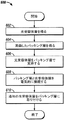
次に図6を参照すると、図1に示すX線検出器100を作製する方法が要約されている。最初に、光受容体層が得られる(ステップ602)。光受容体層は、周辺部で界接し、光受容体及び周辺部内に層間接続点を含む。光受容体層は、例えば、シリコン結晶上に製作した複数のフォトダイオードとすることができる。
Referring now to FIG. 6, a method for making the
また、湾曲したバッキング層も得られる(ステップ604)。バッキング層は、上述のように、又は以下に図7に関して述べるように作製されたセラミック又は金属のバッキング層とすることができる。従って、湾曲したバッキング層は、ルーティング接続点と、任意選択的に光受容体層の周りにおける周辺部のみの接続を超える有意な信号ルーティング機能をもたらす内部接続トレースとを含む。 A curved backing layer is also obtained (step 604). The backing layer may be a ceramic or metal backing layer made as described above or as described below with respect to FIG. Thus, the curved backing layer includes routing connection points and, optionally, interconnect traces that provide significant signal routing functions beyond the peripheral connections only around the photoreceptor layer.
次に、光受容体層は、バッキング層に取り付けられて支持される(ステップ606)。このために、ポリマー層を光受容体層とバッキング層との間に配置することができる。或いは、バッキング層は、特定の光受容体層の平坦な裏面を適合させる多角形の平坦な表面を含むことができる。 The photoreceptor layer is then attached and supported on the backing layer (step 606). For this purpose, a polymer layer can be arranged between the photoreceptor layer and the backing layer. Alternatively, the backing layer can include a polygonal flat surface that conforms to the flat backside of a particular photoreceptor layer.
次いで、光受容体層とバッキング層との間に電気的接続性が確立する(ステップ708)。例えば、層間接続点は、バッキング層上のルーティング接続点に接触し、又はこれと結合し、又はこれにはんだ付けすることができる。その後、追加の光受容体層を同様の方法でバッキング層に取り付けて、より大きいX線イメージング・アレイを形成することができる(ステップ610)。 Electrical connectivity is then established between the photoreceptor layer and the backing layer (step 708). For example, an interlayer connection point can contact, bond to, or be soldered to a routing connection point on the backing layer. An additional photoreceptor layer can then be attached to the backing layer in a similar manner to form a larger x-ray imaging array (step 610).
次に図7を参照すると、図4に示すX線検出器400を製作する方法が要約されている。薄いガラス層を、加工中の取り扱い及び最終製品を支持するポリマー層に結合する(ステップ702)。結果として得られる基板は、予め選択された品質仕様に適合することを保証するために原材料として試験可能である。その後、化学蒸着(CVD)工程及びフォトリソグラフィック・マスキング工程により、ガラス面上に光検出体の電子層が作られる(ステップ704)。該電子層は、絶縁層又は設計指定の他の層のみならず、フォトダイオード、FET、及び電子画像獲得用の走査線とデータ線のマトリックスを含むことができる。薄いガラス層は堆積工程中に典型的には平坦な状態に保持され、その結果として既存のCVD工程及びフォトリソグラフィック・マスキング工程を用いて電子層を作ることができる点に留意されたい。得られたサブアセンブリは、品質管理の目的で試験可能である。
Referring now to FIG. 7, a method for fabricating the
更に、バッキング構造体を製作する(ステップ706)。例えば、バッキング層をセラミックのバッキング層とする場合、セラミックがまだ可撓性の(「グリーン・テープ」)段階にあるときに、ドリル工程によりバッキング層を貫通するバイア用の穴を生成することができる。また、セラミックが焼成された後に金属トレースが所望される箇所には全て、金属化インク(例えばタングステン・インク)がこの段階でセラミック上に堆積される。バッキング層は次いで、X線検出器用の最終形態に対して所望される湾曲した形状に形成される。次いで、セラミックが焼成され、その後に、硬質の形態となる。次いで、金属化工程により、金属のスルー・バイア、並びにセラミック表面上の導電経路が形成される。複数の薄いバッキング層(説明されたように個々に準備された)を垂直に積層してバッキング層全体を形成することができる。バッキング層全体は、複数の積層された薄い層を含むことができる。 Further, a backing structure is manufactured (step 706). For example, if the backing layer is a ceramic backing layer, the drilling process may create via holes through the backing layer when the ceramic is still in the flexible ("green tape") stage. it can. Also, metalized ink (eg, tungsten ink) is deposited on the ceramic at this stage wherever metal traces are desired after the ceramic is fired. The backing layer is then formed into the desired curved shape for the final form for the x-ray detector. The ceramic is then fired and then into a hard form. The metallization process then forms metal through-vias as well as conductive paths on the ceramic surface. A plurality of thin backing layers (prepared individually as described) can be stacked vertically to form the entire backing layer. The entire backing layer can include multiple stacked thin layers.
次に、可撓性の薄いガラス及びポリマー基板が、所望の幾何寸法の最終的なX線検出器形状に湾曲される(ステップ708)。1つの製作工程において、湾曲は、真空を用いてバッキング層(すでに所望の形状を有する)に押し付けて薄いガラス及びポリマー基板を引き、次いで薄いガラス及びポリマー基板をバッキング層に結合することにより達成することができる。この形状整形及び結合工程の間に薄いガラス及びポリマー基板をバッキング層に押しつけるのに役立つ真空の代わりに又はそれに加えてガス圧力を用いることができる。 Next, the flexible thin glass and polymer substrate is bent into the final X-ray detector shape of the desired geometric dimensions (step 708). In one fabrication process, bending is achieved by using a vacuum to pull the thin glass and polymer substrate against the backing layer (which already has the desired shape) and then bonding the thin glass and polymer substrate to the backing layer. be able to. Gas pressure can be used in place of or in addition to the vacuum that helps to push the thin glass and polymer substrate against the backing layer during this shaping and bonding process.
本工程では、次に、追加の層を薄いガラス層の上に堆積することができる(ステップ710)。例えば、CVD工程により、薄いガラス層の上にシンチレータ層、封止層などを堆積することができる。シンチレータ層は一般的に、薄いガラス層が湾曲された後に堆積され、その結果、シンチレータの脆弱な針形状の結晶(一般的にタリウムがドープされたCsI)が、破壊されないように、又は共に圧迫されて層間剥離が生じないようにする。 The process can then deposit additional layers on the thin glass layer (step 710). For example, a scintillator layer, a sealing layer, and the like can be deposited on a thin glass layer by a CVD process. The scintillator layer is typically deposited after the thin glass layer is curved so that the fragile needle-shaped crystals of the scintillator (typically CsI doped with thallium) are not destroyed or pressed together To prevent delamination.
シンチレータ層及び任意の後続の層のCVDが完了すると、検出器に嵌合するように湾曲されたカバーを、所定の位置に取り付けて結合する(ステップ712)。カバーは、X線検出器を封止して、シンチレータ層により湿気が吸収されるのを防止する。X線検出器は、このレベルにおいて試験可能である。検出器は次いで、フレックス回路接続により画像検出器組立体の残りの部分に接続することができる。この際に、データ読み出しモジュール及び走査モジュールをX線検出器の縁部に沿って取り付けることができる(ステップ714)。図5を参照して上述したように、次いで複数の個々のX線検出器タイルを1つ又はそれ以上の軸に沿って配列し、より大きい検出器を形成することができる(ステップ716)。 When CVD of the scintillator layer and any subsequent layers is complete, a cover that is curved to fit the detector is attached and bonded in place (step 712). The cover seals the X-ray detector and prevents moisture from being absorbed by the scintillator layer. X-ray detectors can be tested at this level. The detector can then be connected to the rest of the image detector assembly by a flex circuit connection. At this time, a data readout module and a scanning module can be attached along the edge of the X-ray detector (step 714). As described above with reference to FIG. 5, a plurality of individual x-ray detector tiles can then be arranged along one or more axes to form a larger detector (step 716).
上述したX線検出器は、汎用X線イメージング・システムと共に用いるのに適している。これらは、例えば、検出器が固定され、放射線源が180度より有意に小さい円弧を通って移動する「部分的な」トモシンセシス、又は、完全な画像再構成のために典型的には少なくとも180度の大きい円弧を通って検出器と放射線源の両方が移動する完全断層撮影のいずれかのCT再構成が可能なX線検出器に更に適している。 The X-ray detector described above is suitable for use with a general purpose X-ray imaging system. These include, for example, “partial” tomosynthesis where the detector is fixed and the radiation source moves through an arc significantly smaller than 180 degrees, or typically at least 180 degrees for complete image reconstruction. It is further suitable for X-ray detectors capable of either CT reconstruction of full tomography where both the detector and the radiation source move through a large arc.
説明したX線検出器は、検出器構成要素、すなわち典型的には相互接続線を有するフォトダイオード及びFET内外への電子信号の高密度ルーティングに対する必要性を満たす。薄いガラス層を用いる場合、ACF結合又は従来のワイヤ結合を有するフレックス回路のようなエッジ接続技術を用いて信号を「ガラスから」取り出すことができる。従って、バッキング層は、セラミックを通してバイアを用いる機会を提供し、また、セラミック内の層中に導電トレースを作り実質的な信号ルーティングの柔軟性をもたらす機会をも提供する。 The described X-ray detector meets the need for high density routing of electronic signals into and out of detector components, ie photodiodes and FETs that typically have interconnect lines. If a thin glass layer is used, the signal can be “out of glass” using edge connection techniques such as flex circuits with ACF bonding or conventional wire bonding. Thus, the backing layer provides an opportunity to use vias through the ceramic and also provides an opportunity to create conductive traces in the layers within the ceramic and provide substantial signal routing flexibility.
本発明の種々の実施形態を説明してきたが、当業者には、本発明の範囲内にある更に多くの実施形態及び実装形態が可能であることは明らかであろう。 While various embodiments of the invention have been described, it will be apparent to those skilled in the art that many more embodiments and implementations are possible that are within the scope of the invention.
400 X線検出器
402 湾曲半径
404 バッキング層
406 カバー層
408 シンチレータ層
410 光受容体層
412 基板層
414 ガラス層
400
Claims (10)
前記ガラス層(414)上に形成された光受容体(410)と、
前記ガラス層(414)を支持する、前記予め選択された湾曲半径(402)に基づいて湾曲したバッキング層(404)と、
を備えるX線検出器(400)。 A curved glass layer (414) based on a preselected radius of curvature (402);
A photoreceptor (410) formed on the glass layer (414);
A backing layer (404) that supports the glass layer (414) and is curved based on the preselected curvature radius (402);
An X-ray detector (400) comprising:
周辺部(202)で界接し、該周辺部内に光受容体と層間接続点(110)とを含む光受容体層(410)と、
前記光受容体層を支持する、予め選択された湾曲半径に基づいて湾曲し且つルーティング接続点(112)を含むバッキング層(404)と、
前記光受容体層と前記バッキング層との間に電気的接続性を確立するための、前記層間接続点と前記ルーティング接続点との間の電気的接続部と、
を備えるX線検出器(400)。 An X-ray detector (400),
A photoreceptor layer (410) that interfaces at the periphery (202) and includes a photoreceptor and an interlayer connection point (110) in the periphery;
A backing layer (404) that supports the photoreceptor layer and is curved based on a preselected radius of curvature and includes a routing connection point (112);
An electrical connection between the interlayer connection point and the routing connection point to establish electrical connectivity between the photoreceptor layer and the backing layer;
An X-ray detector (400) comprising:
周辺部で界接し、且つ該周辺部内に光受容体と層間接続点とを備える光受容体層を得る段階(602)と、
予め選択された湾曲半径に基づいて湾曲し且つルーティング接続点を備えるバッキング層を得る段階(604)と、
前記光受容体層を前記バッキング層で支持する段階(606)と、
前記層間接続点と前記ルーティング接続点との間に電気的接続を確立することにより前記光受容体層を前記バッキング層に接続する段階(608)と、
を含む方法。 A method of manufacturing an X-ray detector,
Obtaining a photoreceptor layer that is in contact at the periphery and comprises a photoreceptor and interlayer connection points in the periphery (602);
Obtaining a backing layer (604) that is curved based on a pre-selected radius of curvature and comprises a routing connection point;
Supporting the photoreceptor layer with the backing layer (606);
Connecting the photoreceptor layer to the backing layer by establishing an electrical connection between the interlayer connection point and the routing connection point (608);
Including methods.
前記支持する段階(606)は、前記複数の光受容体層が前記予め選択された湾曲半径に従うように前記バッキング層で前記複数の光受容体層を支持する段階を含み、
前記接続する段階(608)は、前記層間接続点と前記ルーティング接続点との間の電気的相互接続を通じて、前記複数の光受容体を前記バッキング層に接続する段階を含む請求項9に記載の方法。 Obtaining the photoreceptor layer (602) comprises obtaining a plurality of photoreceptor layers, each comprising an interlayer connection point;
The supporting step (606) includes supporting the plurality of photoreceptor layers with the backing layer such that the plurality of photoreceptor layers follow the pre-selected radius of curvature;
The connecting (608) of claim 9, wherein connecting the plurality of photoreceptors to the backing layer through an electrical interconnection between the interlayer connection point and the routing connection point. Method.
Applications Claiming Priority (1)
| Application Number | Priority Date | Filing Date | Title |
|---|---|---|---|
| US10/452,460 US6982424B2 (en) | 2003-06-02 | 2003-06-02 | X-ray and CT image detector |
Publications (3)
| Publication Number | Publication Date |
|---|---|
| JP2004361402A true JP2004361402A (en) | 2004-12-24 |
| JP2004361402A5 JP2004361402A5 (en) | 2007-07-12 |
| JP4647938B2 JP4647938B2 (en) | 2011-03-09 |
Family
ID=33452003
Family Applications (1)
| Application Number | Title | Priority Date | Filing Date |
|---|---|---|---|
| JP2004162780A Expired - Fee Related JP4647938B2 (en) | 2003-06-02 | 2004-06-01 | How to make an X-ray detector |
Country Status (3)
| Country | Link |
|---|---|
| US (1) | US6982424B2 (en) |
| JP (1) | JP4647938B2 (en) |
| DE (1) | DE102004026948A1 (en) |
Cited By (9)
| Publication number | Priority date | Publication date | Assignee | Title |
|---|---|---|---|---|
| JP2007101256A (en) * | 2005-09-30 | 2007-04-19 | Fujifilm Corp | X-ray imaging apparatus and X-ray CT apparatus |
| KR101111011B1 (en) | 2008-12-26 | 2012-02-15 | 연세대학교 산학협력단 | Multi-layered Flat Panel Detector and 3D Position Detection Method for Gamma Ray Image Measurement |
| JP2012081264A (en) * | 2010-10-11 | 2012-04-26 | General Electric Co <Ge> | Multi-faceted tileable detector for volumetric computed tomography imaging |
| JP2013504057A (en) * | 2009-09-08 | 2013-02-04 | コーニンクレッカ フィリップス エレクトロニクス エヌ ヴィ | Imaging measurement system with printed photodetector array |
| CN102918418A (en) * | 2010-05-25 | 2013-02-06 | 富士胶片株式会社 | Radiological imaging device |
| WO2017145578A1 (en) * | 2016-02-22 | 2017-08-31 | ソニー株式会社 | Image pickup device, image pickup display system, and display device |
| JP2018508758A (en) * | 2015-01-14 | 2018-03-29 | ゼネラル・エレクトリック・カンパニイ | Flexible X-ray detector and manufacturing method thereof |
| KR20190054363A (en) * | 2017-11-13 | 2019-05-22 | 주식회사 토비스 | A method of manufacturing a curved detector and A curved detector |
| JP2023014759A (en) * | 2021-07-19 | 2023-01-31 | 富士フイルム株式会社 | Radiation detector and radiographic device |
Families Citing this family (28)
| Publication number | Priority date | Publication date | Assignee | Title |
|---|---|---|---|---|
| IL143851A0 (en) * | 2001-06-19 | 2002-04-21 | Real Time Radiography Ltd | Systems for detection, imaging and absorption of high energy radiation |
| US20050017182A1 (en) * | 2003-07-25 | 2005-01-27 | Siemens Medical Solutions Usa, Inc. | Registered collimator device for nuclear imaging camera and method of forming the same |
| US7476040B2 (en) * | 2004-02-02 | 2009-01-13 | Jds Uniphase Corporation | Compact optical sub-assembly with ceramic package |
| GB0504415D0 (en) | 2005-03-03 | 2005-04-06 | E2V Tech Uk Ltd | Non-planar x-ray sensor |
| US7291842B2 (en) * | 2005-06-14 | 2007-11-06 | Varian Medical Systems Technologies, Inc. | Photoconductor imagers with sandwich structure |
| DE102006002083B4 (en) * | 2006-01-16 | 2009-06-10 | Siemens Ag | Holder with x-ray detector |
| US7687790B2 (en) * | 2007-06-07 | 2010-03-30 | General Electric Company | EMI shielding of digital x-ray detectors with non-metallic enclosures |
| WO2009024895A2 (en) * | 2007-08-22 | 2009-02-26 | Koninklijke Philips Electronics N.V. | Reflector and light collimator arrangement for improved light collection in scintillation detectors |
| US7945019B2 (en) * | 2008-09-29 | 2011-05-17 | Mir Medical Imaging Research Holding Gmbh | Method and device for thermal breast tumor treatment with 3D monitoring function |
| WO2010058309A2 (en) | 2008-11-18 | 2010-05-27 | Koninklijke Philips Electronics N.V. | Spectral imaging detector |
| US20100128843A1 (en) * | 2008-11-22 | 2010-05-27 | Mir Medical Imaging Research Holding Gmbh | Device for Locating a Female Breast for Diagnostic Imaging and Intervention |
| US8525119B2 (en) * | 2009-05-20 | 2013-09-03 | Koninklijke Philips N. V. | Detector array with pre-focused anti-scatter grid |
| BR112012014166A2 (en) * | 2009-12-15 | 2016-05-17 | Koninkl Philips Electronics Nv | detector image clipping of an imaging system and method |
| US8399847B2 (en) | 2010-11-11 | 2013-03-19 | General Electric Company | Ruggedized enclosure for a radiographic device |
| JP2013050364A (en) * | 2011-08-30 | 2013-03-14 | Fujifilm Corp | Radiation image detector |
| US9935152B2 (en) | 2012-12-27 | 2018-04-03 | General Electric Company | X-ray detector having improved noise performance |
| US9917133B2 (en) | 2013-12-12 | 2018-03-13 | General Electric Company | Optoelectronic device with flexible substrate |
| US10732131B2 (en) | 2014-03-13 | 2020-08-04 | General Electric Company | Curved digital X-ray detector for weld inspection |
| US9515276B2 (en) | 2014-09-02 | 2016-12-06 | General Electric Company | Organic X-ray detector and X-ray systems |
| US9689997B2 (en) | 2014-09-04 | 2017-06-27 | General Electric Company | Systems and methods for modular imaging detectors |
| US9535173B2 (en) | 2014-09-11 | 2017-01-03 | General Electric Company | Organic x-ray detector and x-ray systems |
| CN105628717B (en) * | 2014-10-30 | 2020-05-19 | 通用电气公司 | Light detectors, X-ray detection devices, and X-ray imaging equipment |
| CN109196385B (en) * | 2016-05-26 | 2023-08-15 | 皇家飞利浦有限公司 | Multifunctional Radiation Detector |
| CN110582708A (en) * | 2017-05-01 | 2019-12-17 | 皇家飞利浦有限公司 | Multilayer Radiation Detector |
| CN110148602B (en) * | 2019-05-07 | 2022-07-19 | 上海奕瑞光电子科技股份有限公司 | X-ray detector |
| US12372672B2 (en) | 2019-10-18 | 2025-07-29 | The University Of North Carolina At Chapel Hill | Membrane-perovskite films, devices, and methods of preparation |
| KR102373241B1 (en) * | 2021-06-15 | 2022-03-15 | 주식회사 디알텍 | Radiation detector and radiation inspection apparatus using the same |
| CN115144417A (en) * | 2022-06-08 | 2022-10-04 | 北京纳米维景科技有限公司 | A flexible CT detector and its static CT system |
Citations (12)
| Publication number | Priority date | Publication date | Assignee | Title |
|---|---|---|---|---|
| JPS6243585A (en) * | 1985-08-21 | 1987-02-25 | Toshiba Corp | Detector for x ray ct |
| JPS6314469A (en) * | 1986-07-07 | 1988-01-21 | Komatsu Ltd | Photosensor array device and its manufacturing method |
| JPS6457871A (en) * | 1987-08-28 | 1989-03-06 | Hitachi Ltd | Image sensor |
| JPH01126584A (en) * | 1987-11-12 | 1989-05-18 | Toshiba Corp | Radiation detector for x ray ct |
| JPH01202989A (en) * | 1988-02-09 | 1989-08-15 | Nec Corp | Solid-state image pickup device |
| JPH0251472A (en) * | 1988-08-12 | 1990-02-21 | Yoshida Kogyo Kk <Ykk> | Firing method for ceramic extruded long shapes |
| JPH0511301U (en) * | 1991-07-26 | 1993-02-12 | 日本板硝子株式会社 | X-ray image sensor |
| JPH0634763A (en) * | 1992-07-17 | 1994-02-10 | Fuji Electric Co Ltd | Radioactive ray detector |
| JPH1095139A (en) * | 1996-07-16 | 1998-04-14 | Ngk Insulators Ltd | Ceramic member |
| JP2000058995A (en) * | 1998-08-11 | 2000-02-25 | Sumitomo Kinzoku Electro Device:Kk | Ceramic circuit board and semiconductor module |
| US6403964B1 (en) * | 1997-12-18 | 2002-06-11 | Simage Oy | Modular imaging apparatus |
| US6510195B1 (en) * | 2001-07-18 | 2003-01-21 | Koninklijke Philips Electronics, N.V. | Solid state x-radiation detector modules and mosaics thereof, and an imaging method and apparatus employing the same |
Family Cites Families (12)
| Publication number | Priority date | Publication date | Assignee | Title |
|---|---|---|---|---|
| US4403939A (en) * | 1979-02-21 | 1983-09-13 | Trustees Boston University | Process and apparatus for producing a molecularly oriented film |
| US5864146A (en) * | 1996-11-13 | 1999-01-26 | University Of Massachusetts Medical Center | System for quantitative radiographic imaging |
| US5315113A (en) * | 1992-09-29 | 1994-05-24 | The Perkin-Elmer Corporation | Scanning and high resolution x-ray photoelectron spectroscopy and imaging |
| US5515411A (en) * | 1993-03-31 | 1996-05-07 | Shimadzu Corporation | X-ray image pickup tube |
| US5686733A (en) * | 1996-03-29 | 1997-11-11 | Mcgill University | Megavoltage imaging method using a combination of a photoreceptor with a high energy photon converter and intensifier |
| EP0816873B1 (en) * | 1996-06-27 | 2002-10-09 | Analogic Corporation | Quadrature transverse computed tomography detection system |
| CA2184667C (en) * | 1996-09-03 | 2000-06-20 | Bradley Trent Polischuk | Multilayer plate for x-ray imaging and method of producing same |
| US6011575A (en) * | 1996-09-10 | 2000-01-04 | Konica Corporation | Image forming apparatus with line-shaped image exposure means |
| US6091795A (en) * | 1997-10-10 | 2000-07-18 | Analogic Corporation | Area detector array for computer tomography scanning system |
| US6139337A (en) | 1997-11-26 | 2000-10-31 | General Electric Company | Elastomeric connection for computed tomography system |
| WO2000062093A1 (en) | 1999-04-14 | 2000-10-19 | Juni Jack E | Single photon emission computed tomography system |
| US20010054723A1 (en) * | 2000-03-17 | 2001-12-27 | Tadashi Narui | Image sensor, method of fabricating the same, and exposure apparatus, measuring device, alignment device, and aberration measuring device using the image sensor |
-
2003
- 2003-06-02 US US10/452,460 patent/US6982424B2/en not_active Expired - Lifetime
-
2004
- 2004-06-01 DE DE102004026948A patent/DE102004026948A1/en not_active Withdrawn
- 2004-06-01 JP JP2004162780A patent/JP4647938B2/en not_active Expired - Fee Related
Patent Citations (12)
| Publication number | Priority date | Publication date | Assignee | Title |
|---|---|---|---|---|
| JPS6243585A (en) * | 1985-08-21 | 1987-02-25 | Toshiba Corp | Detector for x ray ct |
| JPS6314469A (en) * | 1986-07-07 | 1988-01-21 | Komatsu Ltd | Photosensor array device and its manufacturing method |
| JPS6457871A (en) * | 1987-08-28 | 1989-03-06 | Hitachi Ltd | Image sensor |
| JPH01126584A (en) * | 1987-11-12 | 1989-05-18 | Toshiba Corp | Radiation detector for x ray ct |
| JPH01202989A (en) * | 1988-02-09 | 1989-08-15 | Nec Corp | Solid-state image pickup device |
| JPH0251472A (en) * | 1988-08-12 | 1990-02-21 | Yoshida Kogyo Kk <Ykk> | Firing method for ceramic extruded long shapes |
| JPH0511301U (en) * | 1991-07-26 | 1993-02-12 | 日本板硝子株式会社 | X-ray image sensor |
| JPH0634763A (en) * | 1992-07-17 | 1994-02-10 | Fuji Electric Co Ltd | Radioactive ray detector |
| JPH1095139A (en) * | 1996-07-16 | 1998-04-14 | Ngk Insulators Ltd | Ceramic member |
| US6403964B1 (en) * | 1997-12-18 | 2002-06-11 | Simage Oy | Modular imaging apparatus |
| JP2000058995A (en) * | 1998-08-11 | 2000-02-25 | Sumitomo Kinzoku Electro Device:Kk | Ceramic circuit board and semiconductor module |
| US6510195B1 (en) * | 2001-07-18 | 2003-01-21 | Koninklijke Philips Electronics, N.V. | Solid state x-radiation detector modules and mosaics thereof, and an imaging method and apparatus employing the same |
Cited By (15)
| Publication number | Priority date | Publication date | Assignee | Title |
|---|---|---|---|---|
| JP2007101256A (en) * | 2005-09-30 | 2007-04-19 | Fujifilm Corp | X-ray imaging apparatus and X-ray CT apparatus |
| KR101111011B1 (en) | 2008-12-26 | 2012-02-15 | 연세대학교 산학협력단 | Multi-layered Flat Panel Detector and 3D Position Detection Method for Gamma Ray Image Measurement |
| JP2013504057A (en) * | 2009-09-08 | 2013-02-04 | コーニンクレッカ フィリップス エレクトロニクス エヌ ヴィ | Imaging measurement system with printed photodetector array |
| CN102918418A (en) * | 2010-05-25 | 2013-02-06 | 富士胶片株式会社 | Radiological imaging device |
| JP2012081264A (en) * | 2010-10-11 | 2012-04-26 | General Electric Co <Ge> | Multi-faceted tileable detector for volumetric computed tomography imaging |
| JP2018508758A (en) * | 2015-01-14 | 2018-03-29 | ゼネラル・エレクトリック・カンパニイ | Flexible X-ray detector and manufacturing method thereof |
| WO2017145578A1 (en) * | 2016-02-22 | 2017-08-31 | ソニー株式会社 | Image pickup device, image pickup display system, and display device |
| KR20190054363A (en) * | 2017-11-13 | 2019-05-22 | 주식회사 토비스 | A method of manufacturing a curved detector and A curved detector |
| WO2019093722A3 (en) * | 2017-11-13 | 2019-06-27 | 주식회사 토비스 | Method for manufacturing curved-surface detector, and curved-surface detector manufactured using the manufacturing method |
| KR102051957B1 (en) | 2017-11-13 | 2019-12-04 | 주식회사 토비스 | A method of manufacturing a curved detector |
| JP2021502560A (en) * | 2017-11-13 | 2021-01-28 | トビス カンパニー リミテッドTovis Co., Ltd. | Manufacturing method of curved surface detector and curved surface detector manufactured by this manufacturing method |
| US11183533B2 (en) | 2017-11-13 | 2021-11-23 | Tovis Co., Ltd. | Method for manufacturing curved-surface detector, and curved-surface detector manufactured using the manufacturing method |
| JP2023014759A (en) * | 2021-07-19 | 2023-01-31 | 富士フイルム株式会社 | Radiation detector and radiographic device |
| US12111430B2 (en) | 2021-07-19 | 2024-10-08 | Fujifilm Corporation | Radiation detector and radiography apparatus |
| JP7636284B2 (en) | 2021-07-19 | 2025-02-26 | 富士フイルム株式会社 | Radiation detector and radiography device |
Also Published As
| Publication number | Publication date |
|---|---|
| US6982424B2 (en) | 2006-01-03 |
| JP4647938B2 (en) | 2011-03-09 |
| DE102004026948A1 (en) | 2004-12-30 |
| US20040238750A1 (en) | 2004-12-02 |
Similar Documents
| Publication | Publication Date | Title |
|---|---|---|
| JP4647938B2 (en) | How to make an X-ray detector | |
| US9000382B2 (en) | Spectral imaging detector | |
| US8710448B2 (en) | Radiation detector array | |
| EP1356317B1 (en) | Back-illuminated photodiodes for computed tomography detectors | |
| US11112509B2 (en) | Multifunctional radiation detector | |
| US6510195B1 (en) | Solid state x-radiation detector modules and mosaics thereof, and an imaging method and apparatus employing the same | |
| US7117588B2 (en) | Method for assembling tiled detectors for ionizing radiation based image detection | |
| CN101214154B (en) | CT detector module structure | |
| US9835733B2 (en) | Apparatus for detecting X-rays | |
| US8575558B2 (en) | Detector array with a through-via interposer | |
| EP3143430B1 (en) | Sensor device and imaging system for detecting radiation signals | |
| EP2034335A1 (en) | Radiation detector and method for manufacturing the same | |
| WO2015033506A1 (en) | Radiation detection device, method for producing same, and radiation detection system | |
| US6559452B1 (en) | Image input apparatus | |
| CN108604591A (en) | Camera device, camera display system and display device | |
| US6946661B2 (en) | Methods and apparatus for X-ray image detector assemblies | |
| US10686003B2 (en) | Radiation detector assembly | |
| JP2008032407A (en) | Scintillator panel and radiation detection apparatus | |
| JP2022129063A (en) | Radiation imaging apparatus and manufacturing method for radiation imaging apparatus and radiation imaging system | |
| JP2002506213A (en) | Semiconductor imaging device |
Legal Events
| Date | Code | Title | Description |
|---|---|---|---|
| A521 | Request for written amendment filed |
Free format text: JAPANESE INTERMEDIATE CODE: A523 Effective date: 20070525 |
|
| A621 | Written request for application examination |
Free format text: JAPANESE INTERMEDIATE CODE: A621 Effective date: 20070525 |
|
| A131 | Notification of reasons for refusal |
Free format text: JAPANESE INTERMEDIATE CODE: A131 Effective date: 20090908 |
|
| A521 | Request for written amendment filed |
Free format text: JAPANESE INTERMEDIATE CODE: A523 Effective date: 20091007 |
|
| RD02 | Notification of acceptance of power of attorney |
Free format text: JAPANESE INTERMEDIATE CODE: A7422 Effective date: 20091007 |
|
| RD04 | Notification of resignation of power of attorney |
Free format text: JAPANESE INTERMEDIATE CODE: A7424 Effective date: 20091007 |
|
| A131 | Notification of reasons for refusal |
Free format text: JAPANESE INTERMEDIATE CODE: A131 Effective date: 20091110 |
|
| A521 | Request for written amendment filed |
Free format text: JAPANESE INTERMEDIATE CODE: A523 Effective date: 20100208 |
|
| A02 | Decision of refusal |
Free format text: JAPANESE INTERMEDIATE CODE: A02 Effective date: 20100420 |
|
| A521 | Request for written amendment filed |
Free format text: JAPANESE INTERMEDIATE CODE: A523 Effective date: 20100715 |
|
| A911 | Transfer to examiner for re-examination before appeal (zenchi) |
Free format text: JAPANESE INTERMEDIATE CODE: A911 Effective date: 20100827 |
|
| TRDD | Decision of grant or rejection written | ||
| A01 | Written decision to grant a patent or to grant a registration (utility model) |
Free format text: JAPANESE INTERMEDIATE CODE: A01 Effective date: 20101116 |
|
| A01 | Written decision to grant a patent or to grant a registration (utility model) |
Free format text: JAPANESE INTERMEDIATE CODE: A01 |
|
| A61 | First payment of annual fees (during grant procedure) |
Free format text: JAPANESE INTERMEDIATE CODE: A61 Effective date: 20101209 |
|
| FPAY | Renewal fee payment (event date is renewal date of database) |
Free format text: PAYMENT UNTIL: 20131217 Year of fee payment: 3 |
|
| R150 | Certificate of patent or registration of utility model |
Ref document number: 4647938 Country of ref document: JP Free format text: JAPANESE INTERMEDIATE CODE: R150 Free format text: JAPANESE INTERMEDIATE CODE: R150 |
|
| R250 | Receipt of annual fees |
Free format text: JAPANESE INTERMEDIATE CODE: R250 |
|
| R250 | Receipt of annual fees |
Free format text: JAPANESE INTERMEDIATE CODE: R250 |
|
| R250 | Receipt of annual fees |
Free format text: JAPANESE INTERMEDIATE CODE: R250 |
|
| R250 | Receipt of annual fees |
Free format text: JAPANESE INTERMEDIATE CODE: R250 |
|
| R250 | Receipt of annual fees |
Free format text: JAPANESE INTERMEDIATE CODE: R250 |
|
| R250 | Receipt of annual fees |
Free format text: JAPANESE INTERMEDIATE CODE: R250 |
|
| R250 | Receipt of annual fees |
Free format text: JAPANESE INTERMEDIATE CODE: R250 |
|
| LAPS | Cancellation because of no payment of annual fees |