JP2004361402A - X線及びct画像検出器 - Google Patents
X線及びct画像検出器 Download PDFInfo
- Publication number
- JP2004361402A JP2004361402A JP2004162780A JP2004162780A JP2004361402A JP 2004361402 A JP2004361402 A JP 2004361402A JP 2004162780 A JP2004162780 A JP 2004162780A JP 2004162780 A JP2004162780 A JP 2004162780A JP 2004361402 A JP2004361402 A JP 2004361402A
- Authority
- JP
- Japan
- Prior art keywords
- layer
- photoreceptor
- backing layer
- ray detector
- connection point
- Prior art date
- Legal status (The legal status is an assumption and is not a legal conclusion. Google has not performed a legal analysis and makes no representation as to the accuracy of the status listed.)
- Granted
Links
- 239000010410 layer Substances 0.000 claims abstract description 225
- 108091008695 photoreceptors Proteins 0.000 claims abstract description 55
- 239000011521 glass Substances 0.000 claims abstract description 34
- 239000011229 interlayer Substances 0.000 claims abstract description 16
- 238000000034 method Methods 0.000 claims description 20
- 239000000919 ceramic Substances 0.000 claims description 18
- 238000004519 manufacturing process Methods 0.000 claims description 4
- 239000004020 conductor Substances 0.000 claims description 2
- 238000002591 computed tomography Methods 0.000 abstract description 16
- 238000003325 tomography Methods 0.000 abstract description 3
- 230000008569 process Effects 0.000 description 11
- 238000003384 imaging method Methods 0.000 description 10
- 229920000642 polymer Polymers 0.000 description 10
- 239000000758 substrate Substances 0.000 description 6
- XUIMIQQOPSSXEZ-UHFFFAOYSA-N Silicon Chemical compound [Si] XUIMIQQOPSSXEZ-UHFFFAOYSA-N 0.000 description 5
- 238000005229 chemical vapour deposition Methods 0.000 description 5
- 239000013078 crystal Substances 0.000 description 5
- 239000011159 matrix material Substances 0.000 description 5
- 229920001721 polyimide Polymers 0.000 description 5
- 229910052710 silicon Inorganic materials 0.000 description 5
- 239000010703 silicon Substances 0.000 description 5
- 239000004642 Polyimide Substances 0.000 description 4
- 230000008901 benefit Effects 0.000 description 4
- 239000000463 material Substances 0.000 description 4
- 229910052751 metal Inorganic materials 0.000 description 4
- 239000002184 metal Substances 0.000 description 4
- 229920000307 polymer substrate Polymers 0.000 description 4
- WFKWXMTUELFFGS-UHFFFAOYSA-N tungsten Chemical compound [W] WFKWXMTUELFFGS-UHFFFAOYSA-N 0.000 description 4
- 229910052721 tungsten Inorganic materials 0.000 description 4
- 239000010937 tungsten Substances 0.000 description 4
- 239000004593 Epoxy Substances 0.000 description 3
- 229910052782 aluminium Inorganic materials 0.000 description 3
- XAGFODPZIPBFFR-UHFFFAOYSA-N aluminium Chemical compound [Al] XAGFODPZIPBFFR-UHFFFAOYSA-N 0.000 description 3
- 229910021417 amorphous silicon Inorganic materials 0.000 description 3
- 238000005452 bending Methods 0.000 description 3
- 238000013170 computed tomography imaging Methods 0.000 description 3
- 230000003287 optical effect Effects 0.000 description 3
- RYGMFSIKBFXOCR-UHFFFAOYSA-N Copper Chemical compound [Cu] RYGMFSIKBFXOCR-UHFFFAOYSA-N 0.000 description 2
- XEEYBQQBJWHFJM-UHFFFAOYSA-N Iron Chemical compound [Fe] XEEYBQQBJWHFJM-UHFFFAOYSA-N 0.000 description 2
- GWEVSGVZZGPLCZ-UHFFFAOYSA-N Titan oxide Chemical compound O=[Ti]=O GWEVSGVZZGPLCZ-UHFFFAOYSA-N 0.000 description 2
- 229910010293 ceramic material Inorganic materials 0.000 description 2
- 239000011248 coating agent Substances 0.000 description 2
- 238000000576 coating method Methods 0.000 description 2
- 229910052802 copper Inorganic materials 0.000 description 2
- 239000010949 copper Substances 0.000 description 2
- 239000011888 foil Substances 0.000 description 2
- 230000000873 masking effect Effects 0.000 description 2
- 230000002093 peripheral effect Effects 0.000 description 2
- 238000002360 preparation method Methods 0.000 description 2
- 230000005855 radiation Effects 0.000 description 2
- 229910052716 thallium Inorganic materials 0.000 description 2
- BKVIYDNLLOSFOA-UHFFFAOYSA-N thallium Chemical compound [Tl] BKVIYDNLLOSFOA-UHFFFAOYSA-N 0.000 description 2
- 229920002799 BoPET Polymers 0.000 description 1
- OKTJSMMVPCPJKN-UHFFFAOYSA-N Carbon Chemical compound [C] OKTJSMMVPCPJKN-UHFFFAOYSA-N 0.000 description 1
- 239000005041 Mylar™ Substances 0.000 description 1
- 239000000853 adhesive Substances 0.000 description 1
- 230000001070 adhesive effect Effects 0.000 description 1
- 239000000956 alloy Substances 0.000 description 1
- 229910045601 alloy Inorganic materials 0.000 description 1
- 230000002238 attenuated effect Effects 0.000 description 1
- 230000015556 catabolic process Effects 0.000 description 1
- 238000012937 correction Methods 0.000 description 1
- 238000005336 cracking Methods 0.000 description 1
- 238000006731 degradation reaction Methods 0.000 description 1
- 230000032798 delamination Effects 0.000 description 1
- 238000005137 deposition process Methods 0.000 description 1
- 238000002059 diagnostic imaging Methods 0.000 description 1
- 238000005553 drilling Methods 0.000 description 1
- 230000008030 elimination Effects 0.000 description 1
- 238000003379 elimination reaction Methods 0.000 description 1
- 230000005669 field effect Effects 0.000 description 1
- 239000012467 final product Substances 0.000 description 1
- 229910002804 graphite Inorganic materials 0.000 description 1
- 239000010439 graphite Substances 0.000 description 1
- 238000003702 image correction Methods 0.000 description 1
- 229910052742 iron Inorganic materials 0.000 description 1
- 230000031700 light absorption Effects 0.000 description 1
- 230000007246 mechanism Effects 0.000 description 1
- 238000001465 metallisation Methods 0.000 description 1
- 238000007747 plating Methods 0.000 description 1
- 238000003908 quality control method Methods 0.000 description 1
- 239000002994 raw material Substances 0.000 description 1
- 230000009467 reduction Effects 0.000 description 1
- 230000002787 reinforcement Effects 0.000 description 1
- 238000007789 sealing Methods 0.000 description 1
- 238000007493 shaping process Methods 0.000 description 1
- 229910052709 silver Inorganic materials 0.000 description 1
- 239000004332 silver Substances 0.000 description 1
- 238000005476 soldering Methods 0.000 description 1
- 239000003351 stiffener Substances 0.000 description 1
- 239000004408 titanium dioxide Substances 0.000 description 1
- 230000002792 vascular Effects 0.000 description 1
Images


Classifications
-
- G—PHYSICS
- G01—MEASURING; TESTING
- G01T—MEASUREMENT OF NUCLEAR OR X-RADIATION
- G01T1/00—Measuring X-radiation, gamma radiation, corpuscular radiation, or cosmic radiation
- G01T1/16—Measuring radiation intensity
- G01T1/20—Measuring radiation intensity with scintillation detectors
- G01T1/2018—Scintillation-photodiode combinations
Landscapes
- Physics & Mathematics (AREA)
- Health & Medical Sciences (AREA)
- Life Sciences & Earth Sciences (AREA)
- General Physics & Mathematics (AREA)
- High Energy & Nuclear Physics (AREA)
- Molecular Biology (AREA)
- Spectroscopy & Molecular Physics (AREA)
- Measurement Of Radiation (AREA)
- Apparatus For Radiation Diagnosis (AREA)
- Solid State Image Pick-Up Elements (AREA)
- Transforming Light Signals Into Electric Signals (AREA)
- Light Receiving Elements (AREA)
Abstract
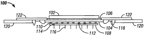
【解決手段】 X線検出器(400)は、予め選択された湾曲半径(402)に基づいて湾曲したガラス層(414)と、該ガラス層上に形成された光受容体(410)と、予め選択された湾曲半径(402)に基づいて湾曲したバッキング層(404)とを含む。バッキング層(404)は、ガラス層(414)を支持する。別の実施形態において、X線検出器は、光受容体と周辺部内に層間接続点とを含み、周辺部で界接する光受容体層を含む。
【選択図】 図4
Description
各層の厚さは、例証として、カバー層406に対しては0.5mm、シンチレータ層408に対しては0.4mmから2mm、非晶質シリコン層及び他の活性電子層412に対しては0.1mmから0.2mm、薄いガラス層414に対しては0.2mmから0.3mm、及びポリマー支持層416に対しては0.5mmから1mmとすることができる。
402 湾曲半径
404 バッキング層
406 カバー層
408 シンチレータ層
410 光受容体層
412 基板層
414 ガラス層
Claims (10)
- 予め選択された湾曲半径(402)に基づいて湾曲したガラス層(414)と、
前記ガラス層(414)上に形成された光受容体(410)と、
前記ガラス層(414)を支持する、前記予め選択された湾曲半径(402)に基づいて湾曲したバッキング層(404)と、
を備えるX線検出器(400)。 - 前記バッキング層(404)はセラミックのバッキング層である請求項1に記載のX線検出器(400)。
- 前記ガラス層(414)と前記バッキング層(404)との間に支持層(416)を更に備える請求項1に記載のX線検出器(400)。
- 前記バッキング層(404)は信号伝導体を更に備える請求項1に記載のX線検出器(400)。
- 前記バッキング層(404)は、複数の積層された薄い層(303)を含む請求項1に記載のX線検出器(400)。
- 前記ガラス層(414)は薄い可撓性のガラス層である請求項1に記載のX線検出器(400)。
- X線検出器(400)であって、
周辺部(202)で界接し、該周辺部内に光受容体と層間接続点(110)とを含む光受容体層(410)と、
前記光受容体層を支持する、予め選択された湾曲半径に基づいて湾曲し且つルーティング接続点(112)を含むバッキング層(404)と、
前記光受容体層と前記バッキング層との間に電気的接続性を確立するための、前記層間接続点と前記ルーティング接続点との間の電気的接続部と、
を備えるX線検出器(400)。 - 前記バッキング層(404)は前記予め選択された湾曲半径に従うように配列された複数の個々の光受容体層を支持する請求項7に記載のX線検出器(400)。
- X線検出器を製作する方法であって、
周辺部で界接し、且つ該周辺部内に光受容体と層間接続点とを備える光受容体層を得る段階(602)と、
予め選択された湾曲半径に基づいて湾曲し且つルーティング接続点を備えるバッキング層を得る段階(604)と、
前記光受容体層を前記バッキング層で支持する段階(606)と、
前記層間接続点と前記ルーティング接続点との間に電気的接続を確立することにより前記光受容体層を前記バッキング層に接続する段階(608)と、
を含む方法。 - 光受容体層を得る前記段階(602)は、各々が層間接続点を備える複数の光受容体層を得る段階を含み、
前記支持する段階(606)は、前記複数の光受容体層が前記予め選択された湾曲半径に従うように前記バッキング層で前記複数の光受容体層を支持する段階を含み、
前記接続する段階(608)は、前記層間接続点と前記ルーティング接続点との間の電気的相互接続を通じて、前記複数の光受容体を前記バッキング層に接続する段階を含む請求項9に記載の方法。
Applications Claiming Priority (1)
| Application Number | Priority Date | Filing Date | Title |
|---|---|---|---|
| US10/452,460 US6982424B2 (en) | 2003-06-02 | 2003-06-02 | X-ray and CT image detector |
Publications (3)
| Publication Number | Publication Date |
|---|---|
| JP2004361402A true JP2004361402A (ja) | 2004-12-24 |
| JP2004361402A5 JP2004361402A5 (ja) | 2007-07-12 |
| JP4647938B2 JP4647938B2 (ja) | 2011-03-09 |
Family
ID=33452003
Family Applications (1)
| Application Number | Title | Priority Date | Filing Date |
|---|---|---|---|
| JP2004162780A Expired - Fee Related JP4647938B2 (ja) | 2003-06-02 | 2004-06-01 | X線検出器を製作する方法 |
Country Status (3)
| Country | Link |
|---|---|
| US (1) | US6982424B2 (ja) |
| JP (1) | JP4647938B2 (ja) |
| DE (1) | DE102004026948A1 (ja) |
Cited By (9)
| Publication number | Priority date | Publication date | Assignee | Title |
|---|---|---|---|---|
| JP2007101256A (ja) * | 2005-09-30 | 2007-04-19 | Fujifilm Corp | X線撮像装置及びx線ct装置 |
| KR101111011B1 (ko) | 2008-12-26 | 2012-02-15 | 연세대학교 산학협력단 | 감마선 영상측정을 위한 다층 평판형 검출기 및 3차원 위치검출방법 |
| JP2012081264A (ja) * | 2010-10-11 | 2012-04-26 | General Electric Co <Ge> | 容積測定計算機式断層写真法撮像用のタイル構成可能な多面検出器 |
| JP2013504057A (ja) * | 2009-09-08 | 2013-02-04 | コーニンクレッカ フィリップス エレクトロニクス エヌ ヴィ | 印刷された光検出器アレイを備えた撮像測定システム |
| CN102918418A (zh) * | 2010-05-25 | 2013-02-06 | 富士胶片株式会社 | 放射线成像装置 |
| WO2017145578A1 (ja) * | 2016-02-22 | 2017-08-31 | ソニー株式会社 | 撮像装置、撮像表示システムおよび表示装置 |
| JP2018508758A (ja) * | 2015-01-14 | 2018-03-29 | ゼネラル・エレクトリック・カンパニイ | 可撓x線検出器およびその製造方法 |
| KR20190054363A (ko) * | 2017-11-13 | 2019-05-22 | 주식회사 토비스 | 곡면 디텍터의 제조방법 및 이 제조방법에 의해 제조된 곡면 디텍터 |
| JP2023014759A (ja) * | 2021-07-19 | 2023-01-31 | 富士フイルム株式会社 | 放射線検出器、および放射線撮影装置 |
Families Citing this family (28)
| Publication number | Priority date | Publication date | Assignee | Title |
|---|---|---|---|---|
| IL143851A0 (en) * | 2001-06-19 | 2002-04-21 | Real Time Radiography Ltd | Systems for detection, imaging and absorption of high energy radiation |
| US20050017182A1 (en) * | 2003-07-25 | 2005-01-27 | Siemens Medical Solutions Usa, Inc. | Registered collimator device for nuclear imaging camera and method of forming the same |
| US7476040B2 (en) * | 2004-02-02 | 2009-01-13 | Jds Uniphase Corporation | Compact optical sub-assembly with ceramic package |
| GB0504415D0 (en) | 2005-03-03 | 2005-04-06 | E2V Tech Uk Ltd | Non-planar x-ray sensor |
| US7291842B2 (en) * | 2005-06-14 | 2007-11-06 | Varian Medical Systems Technologies, Inc. | Photoconductor imagers with sandwich structure |
| DE102006002083B4 (de) * | 2006-01-16 | 2009-06-10 | Siemens Ag | Halterung mit Röntgendetektor |
| US7687790B2 (en) * | 2007-06-07 | 2010-03-30 | General Electric Company | EMI shielding of digital x-ray detectors with non-metallic enclosures |
| WO2009024895A2 (en) * | 2007-08-22 | 2009-02-26 | Koninklijke Philips Electronics N.V. | Reflector and light collimator arrangement for improved light collection in scintillation detectors |
| US7945019B2 (en) * | 2008-09-29 | 2011-05-17 | Mir Medical Imaging Research Holding Gmbh | Method and device for thermal breast tumor treatment with 3D monitoring function |
| WO2010058309A2 (en) | 2008-11-18 | 2010-05-27 | Koninklijke Philips Electronics N.V. | Spectral imaging detector |
| US20100128843A1 (en) * | 2008-11-22 | 2010-05-27 | Mir Medical Imaging Research Holding Gmbh | Device for Locating a Female Breast for Diagnostic Imaging and Intervention |
| US8525119B2 (en) * | 2009-05-20 | 2013-09-03 | Koninklijke Philips N. V. | Detector array with pre-focused anti-scatter grid |
| BR112012014166A2 (pt) * | 2009-12-15 | 2016-05-17 | Koninkl Philips Electronics Nv | recorte de imagem do detector de um sistema de geração de imagens e método |
| US8399847B2 (en) | 2010-11-11 | 2013-03-19 | General Electric Company | Ruggedized enclosure for a radiographic device |
| JP2013050364A (ja) * | 2011-08-30 | 2013-03-14 | Fujifilm Corp | 放射線画像検出装置 |
| US9935152B2 (en) | 2012-12-27 | 2018-04-03 | General Electric Company | X-ray detector having improved noise performance |
| US9917133B2 (en) | 2013-12-12 | 2018-03-13 | General Electric Company | Optoelectronic device with flexible substrate |
| US10732131B2 (en) | 2014-03-13 | 2020-08-04 | General Electric Company | Curved digital X-ray detector for weld inspection |
| US9515276B2 (en) | 2014-09-02 | 2016-12-06 | General Electric Company | Organic X-ray detector and X-ray systems |
| US9689997B2 (en) | 2014-09-04 | 2017-06-27 | General Electric Company | Systems and methods for modular imaging detectors |
| US9535173B2 (en) | 2014-09-11 | 2017-01-03 | General Electric Company | Organic x-ray detector and x-ray systems |
| CN105628717B (zh) * | 2014-10-30 | 2020-05-19 | 通用电气公司 | 光检测器、x射线检测装置和x射线成像设备 |
| CN109196385B (zh) * | 2016-05-26 | 2023-08-15 | 皇家飞利浦有限公司 | 多功能辐射检测器 |
| CN110582708A (zh) * | 2017-05-01 | 2019-12-17 | 皇家飞利浦有限公司 | 多层辐射探测器 |
| CN110148602B (zh) * | 2019-05-07 | 2022-07-19 | 上海奕瑞光电子科技股份有限公司 | 一种x射线探测器 |
| US12372672B2 (en) | 2019-10-18 | 2025-07-29 | The University Of North Carolina At Chapel Hill | Membrane-perovskite films, devices, and methods of preparation |
| KR102373241B1 (ko) * | 2021-06-15 | 2022-03-15 | 주식회사 디알텍 | 방사선 디텍터 및 이를 포함하는 방사선 검사장치 |
| CN115144417A (zh) * | 2022-06-08 | 2022-10-04 | 北京纳米维景科技有限公司 | 一种柔性ct探测器及其静态ct系统 |
Citations (12)
| Publication number | Priority date | Publication date | Assignee | Title |
|---|---|---|---|---|
| JPS6243585A (ja) * | 1985-08-21 | 1987-02-25 | Toshiba Corp | X線ct用検出器 |
| JPS6314469A (ja) * | 1986-07-07 | 1988-01-21 | Komatsu Ltd | フオトセンサアレイ装置およびその製造方法 |
| JPS6457871A (en) * | 1987-08-28 | 1989-03-06 | Hitachi Ltd | Image sensor |
| JPH01126584A (ja) * | 1987-11-12 | 1989-05-18 | Toshiba Corp | X線ct用放射線検出器 |
| JPH01202989A (ja) * | 1988-02-09 | 1989-08-15 | Nec Corp | 固体撮像装置 |
| JPH0251472A (ja) * | 1988-08-12 | 1990-02-21 | Yoshida Kogyo Kk <Ykk> | セラミックス押出長尺形材の焼成方法 |
| JPH0511301U (ja) * | 1991-07-26 | 1993-02-12 | 日本板硝子株式会社 | X線イメージセンサ |
| JPH0634763A (ja) * | 1992-07-17 | 1994-02-10 | Fuji Electric Co Ltd | 放射線検出器 |
| JPH1095139A (ja) * | 1996-07-16 | 1998-04-14 | Ngk Insulators Ltd | セラミック部材 |
| JP2000058995A (ja) * | 1998-08-11 | 2000-02-25 | Sumitomo Kinzoku Electro Device:Kk | セラミック回路基板及び半導体モジュール |
| US6403964B1 (en) * | 1997-12-18 | 2002-06-11 | Simage Oy | Modular imaging apparatus |
| US6510195B1 (en) * | 2001-07-18 | 2003-01-21 | Koninklijke Philips Electronics, N.V. | Solid state x-radiation detector modules and mosaics thereof, and an imaging method and apparatus employing the same |
Family Cites Families (12)
| Publication number | Priority date | Publication date | Assignee | Title |
|---|---|---|---|---|
| US4403939A (en) * | 1979-02-21 | 1983-09-13 | Trustees Boston University | Process and apparatus for producing a molecularly oriented film |
| US5864146A (en) * | 1996-11-13 | 1999-01-26 | University Of Massachusetts Medical Center | System for quantitative radiographic imaging |
| US5315113A (en) * | 1992-09-29 | 1994-05-24 | The Perkin-Elmer Corporation | Scanning and high resolution x-ray photoelectron spectroscopy and imaging |
| US5515411A (en) * | 1993-03-31 | 1996-05-07 | Shimadzu Corporation | X-ray image pickup tube |
| US5686733A (en) * | 1996-03-29 | 1997-11-11 | Mcgill University | Megavoltage imaging method using a combination of a photoreceptor with a high energy photon converter and intensifier |
| EP0816873B1 (en) * | 1996-06-27 | 2002-10-09 | Analogic Corporation | Quadrature transverse computed tomography detection system |
| CA2184667C (en) * | 1996-09-03 | 2000-06-20 | Bradley Trent Polischuk | Multilayer plate for x-ray imaging and method of producing same |
| US6011575A (en) * | 1996-09-10 | 2000-01-04 | Konica Corporation | Image forming apparatus with line-shaped image exposure means |
| US6091795A (en) * | 1997-10-10 | 2000-07-18 | Analogic Corporation | Area detector array for computer tomography scanning system |
| US6139337A (en) | 1997-11-26 | 2000-10-31 | General Electric Company | Elastomeric connection for computed tomography system |
| WO2000062093A1 (en) | 1999-04-14 | 2000-10-19 | Juni Jack E | Single photon emission computed tomography system |
| US20010054723A1 (en) * | 2000-03-17 | 2001-12-27 | Tadashi Narui | Image sensor, method of fabricating the same, and exposure apparatus, measuring device, alignment device, and aberration measuring device using the image sensor |
-
2003
- 2003-06-02 US US10/452,460 patent/US6982424B2/en not_active Expired - Lifetime
-
2004
- 2004-06-01 DE DE102004026948A patent/DE102004026948A1/de not_active Withdrawn
- 2004-06-01 JP JP2004162780A patent/JP4647938B2/ja not_active Expired - Fee Related
Patent Citations (12)
| Publication number | Priority date | Publication date | Assignee | Title |
|---|---|---|---|---|
| JPS6243585A (ja) * | 1985-08-21 | 1987-02-25 | Toshiba Corp | X線ct用検出器 |
| JPS6314469A (ja) * | 1986-07-07 | 1988-01-21 | Komatsu Ltd | フオトセンサアレイ装置およびその製造方法 |
| JPS6457871A (en) * | 1987-08-28 | 1989-03-06 | Hitachi Ltd | Image sensor |
| JPH01126584A (ja) * | 1987-11-12 | 1989-05-18 | Toshiba Corp | X線ct用放射線検出器 |
| JPH01202989A (ja) * | 1988-02-09 | 1989-08-15 | Nec Corp | 固体撮像装置 |
| JPH0251472A (ja) * | 1988-08-12 | 1990-02-21 | Yoshida Kogyo Kk <Ykk> | セラミックス押出長尺形材の焼成方法 |
| JPH0511301U (ja) * | 1991-07-26 | 1993-02-12 | 日本板硝子株式会社 | X線イメージセンサ |
| JPH0634763A (ja) * | 1992-07-17 | 1994-02-10 | Fuji Electric Co Ltd | 放射線検出器 |
| JPH1095139A (ja) * | 1996-07-16 | 1998-04-14 | Ngk Insulators Ltd | セラミック部材 |
| US6403964B1 (en) * | 1997-12-18 | 2002-06-11 | Simage Oy | Modular imaging apparatus |
| JP2000058995A (ja) * | 1998-08-11 | 2000-02-25 | Sumitomo Kinzoku Electro Device:Kk | セラミック回路基板及び半導体モジュール |
| US6510195B1 (en) * | 2001-07-18 | 2003-01-21 | Koninklijke Philips Electronics, N.V. | Solid state x-radiation detector modules and mosaics thereof, and an imaging method and apparatus employing the same |
Cited By (15)
| Publication number | Priority date | Publication date | Assignee | Title |
|---|---|---|---|---|
| JP2007101256A (ja) * | 2005-09-30 | 2007-04-19 | Fujifilm Corp | X線撮像装置及びx線ct装置 |
| KR101111011B1 (ko) | 2008-12-26 | 2012-02-15 | 연세대학교 산학협력단 | 감마선 영상측정을 위한 다층 평판형 검출기 및 3차원 위치검출방법 |
| JP2013504057A (ja) * | 2009-09-08 | 2013-02-04 | コーニンクレッカ フィリップス エレクトロニクス エヌ ヴィ | 印刷された光検出器アレイを備えた撮像測定システム |
| CN102918418A (zh) * | 2010-05-25 | 2013-02-06 | 富士胶片株式会社 | 放射线成像装置 |
| JP2012081264A (ja) * | 2010-10-11 | 2012-04-26 | General Electric Co <Ge> | 容積測定計算機式断層写真法撮像用のタイル構成可能な多面検出器 |
| JP2018508758A (ja) * | 2015-01-14 | 2018-03-29 | ゼネラル・エレクトリック・カンパニイ | 可撓x線検出器およびその製造方法 |
| WO2017145578A1 (ja) * | 2016-02-22 | 2017-08-31 | ソニー株式会社 | 撮像装置、撮像表示システムおよび表示装置 |
| KR20190054363A (ko) * | 2017-11-13 | 2019-05-22 | 주식회사 토비스 | 곡면 디텍터의 제조방법 및 이 제조방법에 의해 제조된 곡면 디텍터 |
| WO2019093722A3 (ko) * | 2017-11-13 | 2019-06-27 | 주식회사 토비스 | 곡면 디텍터의 제조방법 및 이 제조방법에 의해 제조된 곡면 디텍터 |
| KR102051957B1 (ko) | 2017-11-13 | 2019-12-04 | 주식회사 토비스 | 곡면 디텍터의 제조방법 |
| JP2021502560A (ja) * | 2017-11-13 | 2021-01-28 | トビス カンパニー リミテッドTovis Co., Ltd. | 曲面検出器の製造方法及びこの製造方法により製造された曲面検出器 |
| US11183533B2 (en) | 2017-11-13 | 2021-11-23 | Tovis Co., Ltd. | Method for manufacturing curved-surface detector, and curved-surface detector manufactured using the manufacturing method |
| JP2023014759A (ja) * | 2021-07-19 | 2023-01-31 | 富士フイルム株式会社 | 放射線検出器、および放射線撮影装置 |
| US12111430B2 (en) | 2021-07-19 | 2024-10-08 | Fujifilm Corporation | Radiation detector and radiography apparatus |
| JP7636284B2 (ja) | 2021-07-19 | 2025-02-26 | 富士フイルム株式会社 | 放射線検出器、および放射線撮影装置 |
Also Published As
| Publication number | Publication date |
|---|---|
| US6982424B2 (en) | 2006-01-03 |
| JP4647938B2 (ja) | 2011-03-09 |
| DE102004026948A1 (de) | 2004-12-30 |
| US20040238750A1 (en) | 2004-12-02 |
Similar Documents
| Publication | Publication Date | Title |
|---|---|---|
| JP4647938B2 (ja) | X線検出器を製作する方法 | |
| US9000382B2 (en) | Spectral imaging detector | |
| US8710448B2 (en) | Radiation detector array | |
| EP1356317B1 (en) | Back-illuminated photodiodes for computed tomography detectors | |
| US11112509B2 (en) | Multifunctional radiation detector | |
| US6510195B1 (en) | Solid state x-radiation detector modules and mosaics thereof, and an imaging method and apparatus employing the same | |
| US7117588B2 (en) | Method for assembling tiled detectors for ionizing radiation based image detection | |
| CN101214154B (zh) | Ct探测器模块构造 | |
| US9835733B2 (en) | Apparatus for detecting X-rays | |
| US8575558B2 (en) | Detector array with a through-via interposer | |
| EP3143430B1 (en) | Sensor device and imaging system for detecting radiation signals | |
| EP2034335A1 (en) | Radiation detector and method for manufacturing the same | |
| WO2015033506A1 (ja) | 放射線検出装置及びその製造方法並びに放射線検出システム | |
| US6559452B1 (en) | Image input apparatus | |
| CN108604591A (zh) | 摄像装置、摄像显示系统和显示装置 | |
| US6946661B2 (en) | Methods and apparatus for X-ray image detector assemblies | |
| US10686003B2 (en) | Radiation detector assembly | |
| JP2008032407A (ja) | シンチレータパネルおよび放射線検出装置 | |
| JP2022129063A (ja) | 放射線撮像装置、放射線撮像装置の製造方法、および放射線撮像システム | |
| JP2002506213A (ja) | 半導体撮像装置 |
Legal Events
| Date | Code | Title | Description |
|---|---|---|---|
| A521 | Request for written amendment filed |
Free format text: JAPANESE INTERMEDIATE CODE: A523 Effective date: 20070525 |
|
| A621 | Written request for application examination |
Free format text: JAPANESE INTERMEDIATE CODE: A621 Effective date: 20070525 |
|
| A131 | Notification of reasons for refusal |
Free format text: JAPANESE INTERMEDIATE CODE: A131 Effective date: 20090908 |
|
| A521 | Request for written amendment filed |
Free format text: JAPANESE INTERMEDIATE CODE: A523 Effective date: 20091007 |
|
| RD02 | Notification of acceptance of power of attorney |
Free format text: JAPANESE INTERMEDIATE CODE: A7422 Effective date: 20091007 |
|
| RD04 | Notification of resignation of power of attorney |
Free format text: JAPANESE INTERMEDIATE CODE: A7424 Effective date: 20091007 |
|
| A131 | Notification of reasons for refusal |
Free format text: JAPANESE INTERMEDIATE CODE: A131 Effective date: 20091110 |
|
| A521 | Request for written amendment filed |
Free format text: JAPANESE INTERMEDIATE CODE: A523 Effective date: 20100208 |
|
| A02 | Decision of refusal |
Free format text: JAPANESE INTERMEDIATE CODE: A02 Effective date: 20100420 |
|
| A521 | Request for written amendment filed |
Free format text: JAPANESE INTERMEDIATE CODE: A523 Effective date: 20100715 |
|
| A911 | Transfer to examiner for re-examination before appeal (zenchi) |
Free format text: JAPANESE INTERMEDIATE CODE: A911 Effective date: 20100827 |
|
| TRDD | Decision of grant or rejection written | ||
| A01 | Written decision to grant a patent or to grant a registration (utility model) |
Free format text: JAPANESE INTERMEDIATE CODE: A01 Effective date: 20101116 |
|
| A01 | Written decision to grant a patent or to grant a registration (utility model) |
Free format text: JAPANESE INTERMEDIATE CODE: A01 |
|
| A61 | First payment of annual fees (during grant procedure) |
Free format text: JAPANESE INTERMEDIATE CODE: A61 Effective date: 20101209 |
|
| FPAY | Renewal fee payment (event date is renewal date of database) |
Free format text: PAYMENT UNTIL: 20131217 Year of fee payment: 3 |
|
| R150 | Certificate of patent or registration of utility model |
Ref document number: 4647938 Country of ref document: JP Free format text: JAPANESE INTERMEDIATE CODE: R150 Free format text: JAPANESE INTERMEDIATE CODE: R150 |
|
| R250 | Receipt of annual fees |
Free format text: JAPANESE INTERMEDIATE CODE: R250 |
|
| R250 | Receipt of annual fees |
Free format text: JAPANESE INTERMEDIATE CODE: R250 |
|
| R250 | Receipt of annual fees |
Free format text: JAPANESE INTERMEDIATE CODE: R250 |
|
| R250 | Receipt of annual fees |
Free format text: JAPANESE INTERMEDIATE CODE: R250 |
|
| R250 | Receipt of annual fees |
Free format text: JAPANESE INTERMEDIATE CODE: R250 |
|
| R250 | Receipt of annual fees |
Free format text: JAPANESE INTERMEDIATE CODE: R250 |
|
| R250 | Receipt of annual fees |
Free format text: JAPANESE INTERMEDIATE CODE: R250 |
|
| LAPS | Cancellation because of no payment of annual fees |