JP2005003473A - Appearance inspection method for weld marks - Google Patents
Appearance inspection method for weld marks Download PDFInfo
- Publication number
- JP2005003473A JP2005003473A JP2003166059A JP2003166059A JP2005003473A JP 2005003473 A JP2005003473 A JP 2005003473A JP 2003166059 A JP2003166059 A JP 2003166059A JP 2003166059 A JP2003166059 A JP 2003166059A JP 2005003473 A JP2005003473 A JP 2005003473A
- Authority
- JP
- Japan
- Prior art keywords
- welding
- marks
- metal plate
- unit block
- mark
- Prior art date
- Legal status (The legal status is an assumption and is not a legal conclusion. Google has not performed a legal analysis and makes no representation as to the accuracy of the status listed.)
- Granted
Links
Images


Landscapes
- Image Analysis (AREA)
- Investigating Materials By The Use Of Optical Means Adapted For Particular Applications (AREA)
- Image Processing (AREA)
Abstract
【課題】本発明の目的は、撮像手段の視野内における溶接痕の位置を合わせる必要のない、すなわち短時間で、かつ精度よく溶接痕の外観を検査することのできる、溶接痕の外観検査方法を提供することにある。
【解決手段】碁盤の目状に複数の溶接痕が形成されてなる金属板表面の溶接痕の外観検査方法において、複数の溶接痕の各中心を結んで形成される領域を単位ブロックとし、該単位ブロックで金属板表面の全溶接痕に対して連続的に単位ブロック分割処理を施して複数のブロックに分割し、分割された各ブロック内の画素輝度値の平均値と積分値を求め、これら平均値と積分値を任意の順番で数列にし、この数列の変化形状を溶接状態良否判定の特徴量とする。
【選択図】 図1An object of the present invention is to provide a method for inspecting the appearance of a welding mark that does not require the position of the welding mark in the field of view of an imaging means, that is, can accurately inspect the appearance of the welding mark in a short time. Is to provide.
In a visual inspection method for welding marks on a surface of a metal plate in which a plurality of welding marks are formed in the shape of a grid, a region formed by connecting the centers of the plurality of welding marks is defined as a unit block. Unit blocks are divided into multiple blocks continuously for all weld marks on the metal plate surface in unit blocks, and the average value and integral value of pixel luminance values in each divided block are obtained. The average value and the integral value are made into a number sequence in an arbitrary order, and the change shape of the number sequence is set as a feature amount for determining the welding state.
[Selection] Figure 1
Description
【0001】
【発明の属する技術分野】
本発明は、例えば、金属板(金属箔を含む)同士を重ねて複数箇所の溶接を施して両者を一体化した金属板において、その表面の溶接痕の外観を検査する、溶接痕の外観検査方法に関するものである。
【0002】
【従来の技術】
二枚の金属板(以下、金属箔を含む)を重ね、これをレーザーや超音波等により溶接する方法が種々の分野で使用されている。具体的には、金属箔からなる導体同士を電気的に接続する場合、接続する導体(金属箔)同士の端末を一部重ね合わせ、これにレーザー溶接機や超音波溶接機等により複数点の溶接を施し、両者を接続している。通常、この溶接は碁盤の目状に複数箇所同時に溶接される。
このようにして得られる金属板表面の溶接状態を検査する場合、溶接痕の間隔が極めて狭いため、目視で検査することは不可能である。そこで従来から、これら溶接の状態、すなわち溶接痕全体を例えばカメラなどの撮像手段で撮影し、これをコンピューターで画像処理して良否を判定する方法が種々検討されている。
【0003】
ところで画像処理に際しては、この種の溶接痕がカメラの視野内のどこにくるかは必ずしも一定でないため、まずその溶接痕の位置を見つける必要がある。
【0004】
そこでこの位置を見つける方法の提案として、例えば特許文献1がある。この特許文献1に記載のものは、溶接時に生成される溶接痕の生成位置を、溶接痕を撮影する入力装置により記憶装置に蓄積された濃淡画像に対して3値化処理を行い、垂直方向軸への輝度の度数投影及び水平方向軸への輝度の度数投影を行い、ある度数以上になる位置(範囲)を求めることにより見つける方法である。
【0005】
特許文献1:特開平11−10373号公報
【0006】
しかしながらこの方法の場合、溶接痕の形状が一定でないためパターンの位置を正確に合わせることが難しい。また溶接痕が複数存在する場合には、射影データが積み重なってしまい、正確な溶接痕のパターン位置情報を得ることができない、という問題がある。
【0007】
前述の問題に鑑み本発明の目的は、撮像手段の視野内における溶接痕の位置を合わせる必要がなく、すなわち短時間で検査でき、かつ精度よく溶接痕の外観を検査することのできる、溶接痕の外観検査方法を提供することにある。
【0008】
【課題を解決するための手段】
前記目的を達成すべく本発明は、碁盤の目状に複数の溶接痕が形成されてなる金属板表面にあって、前記溶接痕の外観検査を画像処理を用いて行う溶接痕の外観検査方法において、複数の溶接痕の各々の中心を結んで形成される領域を単位ブロックとし、該単位ブロックで前記金属板表面のすべての溶接痕に対して連続的に単位ブロック分割処理を施して複数のブロックに分割し、分割された各ブロック内の画素輝度値の平均値と積分値を求め、これら平均値と積分値を任意の順番で数列にし、この数列の変化形状を溶接状態良否判定の特徴量とすることを特徴としている。
【0009】
このようにしてなる本発明によれば、複数の溶接痕の各々の中心を結んで形成される領域を単位ブロックとし、該単位ブロックで前記金属板表面のすべての溶接痕に対して連続的に単位ブロック分割処理を施して複数のブロックに分割しているので、各ブロック内には一定個数の溶接痕が存在するため、背景(ブロック内の溶接痕以外の部分)が一定の特徴を示すと仮定すればブロック全体の特徴を把握することにより溶接痕の特徴を把握することが可能であり、ブロックのサイズで溶接痕の画素ズレによる影響を吸収することができ、従来の方法のもののように溶接痕の正確な位置合わせが不要となる。
【0010】
また本発明では、分割された各ブロック内の画素輝度値の平均値と積分値を求め、これら平均値と積分値を任意の順番で数列にし、この数列の変化形状を溶接状態良否判定の特徴量としている。
そのため、例えば予め良品の画像データからマハラノビス空間を作成しておけば、前述して得た検査対象製品の特徴量を用いて前記マハラノビス空間とのマハラノビス距離を計算し、該計算されたマハラノビス距離を所定の閾値と比較するだけで溶接痕の良否を簡単に、かつ精度よく判定することができる。
【0011】
【発明の実施の形態】
以下に本発明の溶接痕の外観検査方法を図面を参照して詳細に説明する。尚、各図は、金属板1と金属板2を重ねて、これに複数箇所の溶接を施した例を示しているが、いずれも金属板2が下で金属板1が上であることを示している。
【0012】
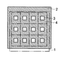
図1(a)は本発明で基礎となる単位ブロックの形と大きさを示している。2枚重ねた金属板1及び金属板2に対して碁盤の目状に複数の溶接痕3が存在している。ここで碁盤の目状に複数の溶接痕が存在する、とは、横方向及び縦方向に所定のピッチで溶接痕が存在する状態をいい、横方向のピッチと縦方向のピッチは同じであってもよいし、異なるピッチであってもよい。
さていまこの溶接痕3を仮にa、b、c、d、e、f、g・・・・とする。金属板1の表面にあってこれらの溶接痕3のうち横方向の隣接する2つの溶接痕e,fと、この2つの溶接痕e、fのうちの一つ、いまこれを溶接痕eとすると、この溶接痕eを含む縦方向の隣接する2つの溶接痕e、gからなる3つの溶接痕e、f、gの各々の中心を結んで形成される直角三角形、または横方向の隣接する2つの溶接痕a、bとこれら2つの溶接痕a、bと隣接する縦方向の2つの溶接痕c、dとからなる4つの溶接痕a、b、c、dの各々の中心を結んで形成される矩形(この場合は長方形)のいずれかを単位ブロック4とする。
【0013】
前記直角三角形か矩形のいずれを単位ブロック4としてもよいが、以下の実施例では溶接痕a、b、c、dの中心を結んで形成される矩形を単位ブロック4として、金属板1の表面のすべての溶接痕3に対して連続的に単位ブロック分割処理を施し、複数のブロックに分割した。これを図1(b)に示す。
【0014】
ここで図2により本発明では溶接痕3の位置合わせを正確に行う必要がない理由を説明する。
図2が示すように、いま仮に単位ブロック4Aにおいて溶接痕3の画素数を9個とする。この単位ブロック4Aから矢印方向に数画素離れた単位ブロック4Bでの溶接痕3の画素数も9個である。換言すると単位ブロック4Aと単位ブロック4Bは溶接痕3(ここでは溶接痕T)に対して、溶接痕3の画素ズレによる影響がない。すなわちブロックのサイズで溶接痕3の画素ズレを吸収している。尚、図2で小さな升目(図2左辺部の升目5)が1画素を示している。
【0015】
本発明ではこのような原理を利用して、溶接痕3の画像の中から画素と形状のズレによる影響に強い特徴量を抽出して、予め溶接状態が良好のものを基準にして溶接痕3の外観の良否の判定基準を作成し、この判定基準と検査対象製品の特徴量とを比較することで検査対象製品の溶接状態の良否を判定する。
【0016】
図3に溶接状態を判定する溶接痕3のモデル画像を示す。前述したように金属板1と金属板2を重ねて溶接した際形成された複数の溶接痕3が金属板1の表面に碁盤の目状に存在している。これを図1(a)で示したような矩形を単位ブロック4として、この単位ブロック4により金属板1の表面上のすべての溶接痕3に対して連続的に単位ブロック分割処理を施し、複数のブロックに分割した。
【0017】
しかる後、単位ブロック4毎に画素輝度値の平均値と積分値を求めた。求めたこれらの値を任意の順番で組み合わせて数列を形成し、この数列の形状を検査対象製品の金属板1表面の特徴量とした。この特徴量抽出の作業の流れを図4のフローチャートに示す。
【0018】
一方、金属板1の表面の溶接状態を判定する場合、予め溶接状態が良好である金属板1を複数枚用意しておき、図5(a)のフローチャートに示す手順に従ってと溶接状態が良好な製品の特徴量の集合体を形成する。
図5(a)が示すように、これら複数枚の良品の金属板1の表面画像をカメラで撮影してその画像を取り込んで、前述した図4の手順と同様にして矩形の単位ブロック4を用いて、金属板1の表面のすべての溶接痕3に対して連続的に単位ブロック分割処理を施し、各ブロック毎に画素輝度値の平均値と積分値を求めた。求めたこれらの値を任意の順番で組み合わせて数列を形成し、この数列の形状を溶接状態が良好な金属板1表面の特徴量の集合体とした。
【0019】
そして前記溶接状態が良好な製品の特徴量の集合体を用いてマハラノビス空間を設定した。
しかる後、図5(b)のフローチャートが示すように、検査対象製品の金属板1の表面から読み取った画像により作成した特徴量、すなわち、図4に示すフローチャートに従って求めた各検査対象製品毎の特徴量を用いて、マハラノビス空間とのマハラノビス距離を計算する。計算したマハラノビス距離を所定の閾値と比較することで金属板1の表面の溶接状態についてその良否を判定する。
【0020】
具体的には、ある検査対象の金属板1の表面画像から得たマハラノビス距離が設定した閾値より大きかった場合には、これを溶接不良と判定し、逆に小さかった場合には、これを良品と判定する。
【0021】
具体的に種々の溶接不良状態に本発明の方法を適用し、その精度を確認した例を図6〜図11で説明する。
まず溶接状態が良好な製品を複数枚用意し、図5(a)のフローチャートに従って溶接状態が良好な製品の特徴量の集合体を形成し、マハラノビス空間を作成した。一方図6〜図11が示すように、溶接状態が良好と思われる製品及び意識的に種々の溶接不良状態を作り出した製品を各々8枚づつ用意した。
【0022】
具体的には図6は溶接状態が良好な製品(事例1)で、図7〜図11は溶接状態が不良な製品である。
因みに、図7は金属板1が一部10が欠けていたため溶接不良を起こした製品(事例2)を示しており、図8は金属板1の表面下方に異物11が付着しているため不良を起こした製品(事例3)を示している。また図9は金属板1の右上方部分に溶接漏れ12が発生した製品(事例4)の状態を示し、図10は全体的に溶接不足の状態を起こした製品(事例5)を示している。
そして図11は金属板1全体が完全に存在しない状態(事例6)、すなわちなんらかの理由で金属板1が金属板2上に乗っていず、金属板2上に溶接をしてしまった状態を示している。
【0023】
前記各事例を示す製品各々8枚について、図5のフローチャートに従って良否判定を行った。その結果を図12に示す。図12が示すように溶接状態が良好な製品を示す事例1は、そのマハラノビス距離が閾値よりも小さいが、溶接不良製品を示す図7〜図11の各事例2〜事例6のものは、いずれもマハラノビス距離が閾値より遥かに大きな値を示していた。このように本発明によれば種々の溶接不良製品を確実に不良と判定できることが確認された。
【0024】
上記実施例では、金属板1表面の溶接の良否判定をマハラノビス空間を設定し、各検査対象製品におけるマハラノビス距離を計算し、その値が閾値より大きいか小さいかで判定を行っているが、例えば図4のフローチャートに従って求めた特徴量を用いて良品のそれとの相関の程度を計算することで溶接状態の良否判定を行ってもよいし、あるいはまた各製品毎にマハタン距離を計算することで、求めた値と閾値を比較して溶接状態の良否を判定することもできる。
【0025】
尚、上記実施例で用いた方法、すなわちマハラノビス距離を計算する方法は、通常MTS法(田口メソッド)と呼ばれているものである。
【0026】
尚、前記実施例では隣接する3個または4個の溶接痕の各々の中心を結んで形成される直角三角形または矩形を単位ブロックとしたが、例えば、隣接する6個の溶接痕3の中心を結んで形成される矩形、あるいはそれ以上の溶接痕の各中心を結んで形成される領域を単位ブロックとすることもできる。
【0027】
【発明の効果】
以上述べたように本発明の溶接痕の外観検査方法によれば、撮像手段内の溶接痕の位置を合わせる必要がない。それ故短時間で溶接痕の外観検査ができ、しかも精度よく溶接痕の外観検査、すなわち溶接状態の良否判定をすることができる。
【図面の簡単な説明】
【図1】本発明の溶接痕の外観検査方法において使用する、単位ブロックの形状及び単位ブロック分割方法の一実施例を示すもので、(a)は単位ブロックの形状を、(b)は単位ブロックによる分割方法を示す図である。
【図2】本発明において、溶接痕の位置合わせが不要である理由を説明するための図である。
【図3】本発明により溶接状態を判定する溶接痕のモデル画像である。
【図4】本発明に用いる検査対象製品の特徴量抽出の作業の流れを示すフローチャートである。
【図5】本発明による溶接状態の良否を判定する手順を示すフローチャートで、(a)は基準となる溶接状態が良好な製品の特徴量の集合体を形成するフローチャートを、(b)は各検査対象製品の溶接状態を(a)で形成したものと比較することで判定を行う手順を示すフローチャートである。
【図6】本発明の判定精度を確認するために使用した溶接状態が良好な製品の平面図である。
【図7】本発明の判定精度を確認するために使用した溶接状態が不良な製品の一例を示す平面図である。
【図8】本発明の判定精度を確認するために使用した溶接状態が不良な製品の一例を示す平面図である。
【図9】本発明の判定精度を確認するために使用した溶接状態が不良な製品の一例を示す平面図である。
【図10】本発明の判定精度を確認するために使用した溶接状態が不良な製品の一例を示す平面図である。
【図11】本発明の判定精度を確認するために使用した溶接状態が不良な製品の一例を示す平面図である。
【図12】前記図6〜図11の各製品についてマハラノビス距離を計算した結果を示すグラフである。
【符号の説明】
1 金属板
2 金属板
3 溶接痕
4 単位ブロック
11 異物
12 溶接漏れ[0001]
BACKGROUND OF THE INVENTION
The present invention, for example, inspects the appearance of the weld mark on the surface of a metal plate (including metal foil) that is overlapped with each other and welded at a plurality of locations to integrate the two, and inspects the appearance of the weld mark on the surface. It is about the method.
[0002]
[Prior art]
A method in which two metal plates (hereinafter, including metal foil) are overlapped and welded by laser, ultrasonic waves, or the like is used in various fields. Specifically, when electrically connecting conductors made of metal foil, the terminals of the conductors (metal foil) to be connected are partially overlapped, and a plurality of points are connected to this by a laser welding machine, an ultrasonic welding machine, or the like. Welding and connecting both. Normally, this welding is performed simultaneously at a plurality of locations in a grid pattern.
When inspecting the welded state of the surface of the metal plate thus obtained, the interval between the welding marks is extremely narrow, so that it is impossible to visually inspect. Therefore, various methods have been studied in the past in which these welding states, that is, the entire welding mark is photographed by an imaging means such as a camera, and the quality is judged by image processing using a computer.
[0003]
By the way, in image processing, where this kind of welding mark comes in the field of view of the camera is not always constant, it is necessary to first find the position of the welding mark.
[0004]
Thus, for example, there is
[0005]
Patent Document 1: Japanese Patent Application Laid-Open No. 11-10373
However, in this method, since the shape of the weld mark is not constant, it is difficult to accurately align the position of the pattern. Further, when there are a plurality of welding traces, projection data is accumulated, and there is a problem that accurate pattern position information of the welding traces cannot be obtained.
[0007]
In view of the foregoing problems, the object of the present invention is to eliminate the need to align the position of the welding mark within the field of view of the imaging means, that is, the welding mark that can be inspected in a short time and can accurately inspect the appearance of the welding mark. It is to provide a visual inspection method.
[0008]
[Means for Solving the Problems]
In order to achieve the above object, the present invention provides a method for inspecting the appearance of a welding mark on a surface of a metal plate in which a plurality of welding marks are formed in a grid pattern, and performing an appearance inspection of the welding marks using image processing. In this case, a region formed by connecting the centers of each of the plurality of welding marks is defined as a unit block, and the unit block is continuously subjected to unit block division processing for all the welding marks on the surface of the metal plate. Dividing into blocks, find the average value and integral value of the pixel luminance values in each divided block, make these average value and integral value in a number sequence in any order, and the change shape of this number sequence is a feature of the welding state pass / fail judgment It is characterized by quantity.
[0009]
According to the present invention thus configured, a region formed by connecting the centers of each of the plurality of welding marks is defined as a unit block, and the unit block continuously applies to all the welding marks on the surface of the metal plate. Since the unit block division processing is performed to divide the block into multiple blocks, there is a certain number of welding marks in each block, so the background (the part other than the welding marks in the block) shows certain characteristics. Assuming that it is possible to grasp the characteristics of the welding marks by grasping the characteristics of the entire block, the influence of pixel displacement of the welding marks can be absorbed by the block size, as in the conventional method Accurate alignment of welding marks is not necessary.
[0010]
Further, in the present invention, an average value and an integral value of pixel luminance values in each of the divided blocks are obtained, the average value and the integral value are made into a number sequence in an arbitrary order, and the change shape of the number sequence is a characteristic of the weld state determination. Amount.
Therefore, for example, if a Mahalanobis space is created in advance from non-defective image data, the Mahalanobis distance from the Mahalanobis space is calculated using the feature quantity of the product to be inspected as described above, and the calculated Mahalanobis distance is calculated. Only by comparing with a predetermined threshold value, the quality of the welding mark can be determined easily and accurately.
[0011]
DETAILED DESCRIPTION OF THE INVENTION
The welding mark appearance inspection method of the present invention will be described below in detail with reference to the drawings. In addition, each figure has shown the example which piled up the
[0012]
FIG. 1A shows the shape and size of a unit block that is the basis of the present invention. A plurality of
Let us assume that the
[0013]
Either the right-angled triangle or the rectangle may be used as the
[0014]
Here, the reason why it is not necessary to accurately align the
As shown in FIG. 2, it is assumed that the number of pixels of the
[0015]
In the present invention, using such a principle, a feature quantity that is strong against the influence of the pixel and shape deviation is extracted from the image of the
[0016]
FIG. 3 shows a model image of the
[0017]
Thereafter, an average value and an integral value of the pixel luminance values were obtained for each
[0018]
On the other hand, when the welding state of the surface of the
As shown in FIG. 5A, the surface images of the plurality of
[0019]
Then, a Mahalanobis space was set by using an assembly of feature quantities of products having a good welded state.
Thereafter, as shown in the flowchart of FIG. 5B, the feature amount created from the image read from the surface of the
[0020]
Specifically, if the Mahalanobis distance obtained from the surface image of the
[0021]
Specific examples of applying the method of the present invention to various welding defects and confirming the accuracy will be described with reference to FIGS.
First, a plurality of products with good welding conditions were prepared, and an assembly of feature quantities of products with good welding conditions was formed according to the flowchart of FIG. 5A to create a Mahalanobis space. On the other hand, as shown in FIG. 6 to FIG. 11, 8 products each having a product that seems to be in a good welding state and products that consciously created various welding failure states were prepared.
[0022]
Specifically, FIG. 6 shows a product with good welding (case 1), and FIGS. 7 to 11 show products with poor welding.
Incidentally, FIG. 7 shows a product (case 2) in which the
FIG. 11 shows a state where the
[0023]
A pass / fail judgment was made on each of the eight products showing each case according to the flowchart of FIG. The result is shown in FIG. As shown in FIG. 12,
[0024]
In the above-described embodiment, the Mahalanobis space is set to determine whether or not the surface of the
[0025]
Note that the method used in the above embodiment, that is, the method of calculating the Mahalanobis distance is usually called the MTS method (Taguchi method).
[0026]
In the above embodiment, the unit block is a right triangle or rectangle formed by connecting the centers of the adjacent three or four welding marks, but for example, the centers of the six adjacent welding marks 3 are defined as the unit block. A rectangle formed by tying, or a region formed by tying the centers of welding marks of more than that can be used as a unit block.
[0027]
【The invention's effect】
As described above, according to the welding mark appearance inspection method of the present invention, it is not necessary to align the position of the welding mark in the imaging means. Therefore, the appearance inspection of the welding mark can be performed in a short time, and the appearance inspection of the welding mark can be accurately performed, that is, the quality of the welding state can be determined.
[Brief description of the drawings]
FIGS. 1A and 1B show an embodiment of a unit block shape and a unit block dividing method used in the welding mark appearance inspection method of the present invention. FIG. 1A shows the shape of a unit block, and FIG. It is a figure which shows the division | segmentation method by a block.
FIG. 2 is a diagram for explaining the reason why alignment of welding marks is unnecessary in the present invention.
FIG. 3 is a model image of a welding mark for determining a welding state according to the present invention.
FIG. 4 is a flowchart showing a flow of work for extracting feature quantities of a product to be inspected used in the present invention.
FIG. 5 is a flowchart showing a procedure for determining the quality of a welding state according to the present invention, wherein (a) is a flowchart for forming a set of feature quantities of products having a good welding state as a reference; It is a flowchart which shows the procedure which determines by comparing the welding state of a test object product with what was formed by (a).
FIG. 6 is a plan view of a product having a good welding state used for confirming the determination accuracy of the present invention.
FIG. 7 is a plan view showing an example of a product with a poor welding state used for confirming the determination accuracy of the present invention.
FIG. 8 is a plan view showing an example of a product with a poor welding state used for confirming the determination accuracy of the present invention.
FIG. 9 is a plan view showing an example of a product with a poor weld state used to confirm the determination accuracy of the present invention.
FIG. 10 is a plan view showing an example of a product with a poor welding state used for confirming the determination accuracy of the present invention.
FIG. 11 is a plan view showing an example of a product with a poor weld state used for confirming the determination accuracy of the present invention.
12 is a graph showing the result of calculating the Mahalanobis distance for each product of FIGS. 6 to 11; FIG.
[Explanation of symbols]
1
Claims (2)
Priority Applications (1)
| Application Number | Priority Date | Filing Date | Title |
|---|---|---|---|
| JP2003166059A JP4429640B2 (en) | 2003-06-11 | 2003-06-11 | Appearance inspection method for weld marks |
Applications Claiming Priority (1)
| Application Number | Priority Date | Filing Date | Title |
|---|---|---|---|
| JP2003166059A JP4429640B2 (en) | 2003-06-11 | 2003-06-11 | Appearance inspection method for weld marks |
Publications (2)
| Publication Number | Publication Date |
|---|---|
| JP2005003473A true JP2005003473A (en) | 2005-01-06 |
| JP4429640B2 JP4429640B2 (en) | 2010-03-10 |
Family
ID=34092315
Family Applications (1)
| Application Number | Title | Priority Date | Filing Date |
|---|---|---|---|
| JP2003166059A Expired - Fee Related JP4429640B2 (en) | 2003-06-11 | 2003-06-11 | Appearance inspection method for weld marks |
Country Status (1)
| Country | Link |
|---|---|
| JP (1) | JP4429640B2 (en) |
Cited By (8)
| Publication number | Priority date | Publication date | Assignee | Title |
|---|---|---|---|---|
| JP2008185395A (en) * | 2007-01-29 | 2008-08-14 | Mitsubishi Heavy Ind Ltd | Mounting substrate visual inspection method |
| JP2009103691A (en) * | 2007-10-04 | 2009-05-14 | Nissan Motor Co Ltd | Ultrasonic bonding monitoring apparatus and method |
| JP2011232302A (en) * | 2010-04-30 | 2011-11-17 | Ricoh Elemex Corp | Image inspection method and image inspection device |
| JP2011232303A (en) * | 2010-04-30 | 2011-11-17 | Ricoh Elemex Corp | Image inspection method and image inspection device |
| JP2012117907A (en) * | 2010-11-30 | 2012-06-21 | Ricoh Elemex Corp | Generation method and inspection device for mahalanobis reference space |
| JP2012117908A (en) * | 2010-11-30 | 2012-06-21 | Ricoh Elemex Corp | Generation method, inspection method, and inspection device for mahalanobis reference space |
| KR101284852B1 (en) | 2011-04-07 | 2013-07-09 | 삼성중공업 주식회사 | Apparatus for inspecting weld toe grinding and methord thereof |
| JP2017003274A (en) * | 2015-06-04 | 2017-01-05 | リコーエレメックス株式会社 | Image inspection device |
-
2003
- 2003-06-11 JP JP2003166059A patent/JP4429640B2/en not_active Expired - Fee Related
Cited By (8)
| Publication number | Priority date | Publication date | Assignee | Title |
|---|---|---|---|---|
| JP2008185395A (en) * | 2007-01-29 | 2008-08-14 | Mitsubishi Heavy Ind Ltd | Mounting substrate visual inspection method |
| JP2009103691A (en) * | 2007-10-04 | 2009-05-14 | Nissan Motor Co Ltd | Ultrasonic bonding monitoring apparatus and method |
| JP2011232302A (en) * | 2010-04-30 | 2011-11-17 | Ricoh Elemex Corp | Image inspection method and image inspection device |
| JP2011232303A (en) * | 2010-04-30 | 2011-11-17 | Ricoh Elemex Corp | Image inspection method and image inspection device |
| JP2012117907A (en) * | 2010-11-30 | 2012-06-21 | Ricoh Elemex Corp | Generation method and inspection device for mahalanobis reference space |
| JP2012117908A (en) * | 2010-11-30 | 2012-06-21 | Ricoh Elemex Corp | Generation method, inspection method, and inspection device for mahalanobis reference space |
| KR101284852B1 (en) | 2011-04-07 | 2013-07-09 | 삼성중공업 주식회사 | Apparatus for inspecting weld toe grinding and methord thereof |
| JP2017003274A (en) * | 2015-06-04 | 2017-01-05 | リコーエレメックス株式会社 | Image inspection device |
Also Published As
| Publication number | Publication date |
|---|---|
| JP4429640B2 (en) | 2010-03-10 |
Similar Documents
| Publication | Publication Date | Title |
|---|---|---|
| KR100744212B1 (en) | System and method for detecting defects on a printed circuit board | |
| KR102918236B1 (en) | Compensation for misalignment of reference during part inspection | |
| JP2742240B2 (en) | Defect detection method in inspection of structure surface | |
| CN101127119B (en) | Pattern detecting device and semiconductor detecting system | |
| JP4230880B2 (en) | Defect inspection method | |
| CN119205735B (en) | A high-speed and high-precision method for measuring appearance defects and circuits of ceramic copper-clad substrates | |
| CN117611528A (en) | PCB image detection method and device | |
| JP4429640B2 (en) | Appearance inspection method for weld marks | |
| JP4954469B2 (en) | Appearance inspection method | |
| Perng et al. | Design and development of a new machine vision wire bonding inspection system | |
| JP2006170922A (en) | Appearance inspection method and apparatus | |
| JP6960252B2 (en) | Maintenance management method for image analyzers and railway equipment parts | |
| JP2006049347A (en) | Component edge detection method, component edge detection program, and inspection apparatus | |
| JP3443083B2 (en) | Method of evaluating dangerous spot information of semiconductor device pattern | |
| JP2010091360A (en) | Method and device for inspecting image | |
| JP4076906B2 (en) | Appearance inspection method | |
| JP3857668B2 (en) | Pattern alignment method | |
| JP2000022326A (en) | Apparatus and method for inspecting solder | |
| JP2982617B2 (en) | Inspection method of print amount of cream solder | |
| CA2397382A1 (en) | Method and system for detecting defects on a printed circuit board | |
| JPH0774730B2 (en) | Appearance inspection method for soldered parts | |
| WO2024166608A1 (en) | Visual inspection method and visual inspection device | |
| CN117853427A (en) | Device appearance defect detection method, device, electronic equipment and storage medium | |
| JPH1048151A (en) | Surface flaw detection method | |
| CN121685650A (en) | Positioning compensation method of AOI equipment and AOI equipment |
Legal Events
| Date | Code | Title | Description |
|---|---|---|---|
| A621 | Written request for application examination |
Free format text: JAPANESE INTERMEDIATE CODE: A621 Effective date: 20060601 |
|
| A977 | Report on retrieval |
Free format text: JAPANESE INTERMEDIATE CODE: A971007 Effective date: 20090130 |
|
| A131 | Notification of reasons for refusal |
Free format text: JAPANESE INTERMEDIATE CODE: A131 Effective date: 20090522 |
|
| A521 | Written amendment |
Free format text: JAPANESE INTERMEDIATE CODE: A523 Effective date: 20090721 |
|
| RD02 | Notification of acceptance of power of attorney |
Free format text: JAPANESE INTERMEDIATE CODE: A7422 Effective date: 20090721 |
|
| A131 | Notification of reasons for refusal |
Free format text: JAPANESE INTERMEDIATE CODE: A131 Effective date: 20090821 |
|
| A521 | Written amendment |
Free format text: JAPANESE INTERMEDIATE CODE: A523 Effective date: 20091020 |
|
| TRDD | Decision of grant or rejection written | ||
| A01 | Written decision to grant a patent or to grant a registration (utility model) |
Free format text: JAPANESE INTERMEDIATE CODE: A01 Effective date: 20091127 |
|
| A01 | Written decision to grant a patent or to grant a registration (utility model) |
Free format text: JAPANESE INTERMEDIATE CODE: A01 |
|
| A61 | First payment of annual fees (during grant procedure) |
Free format text: JAPANESE INTERMEDIATE CODE: A61 Effective date: 20091216 |
|
| FPAY | Renewal fee payment (event date is renewal date of database) |
Free format text: PAYMENT UNTIL: 20121225 Year of fee payment: 3 |
|
| FPAY | Renewal fee payment (event date is renewal date of database) |
Free format text: PAYMENT UNTIL: 20121225 Year of fee payment: 3 |
|
| FPAY | Renewal fee payment (event date is renewal date of database) |
Free format text: PAYMENT UNTIL: 20131225 Year of fee payment: 4 |
|
| LAPS | Cancellation because of no payment of annual fees |