JP2005071237A - Semiconductor integrated circuit device - Google Patents
Semiconductor integrated circuit device Download PDFInfo
- Publication number
- JP2005071237A JP2005071237A JP2003302884A JP2003302884A JP2005071237A JP 2005071237 A JP2005071237 A JP 2005071237A JP 2003302884 A JP2003302884 A JP 2003302884A JP 2003302884 A JP2003302884 A JP 2003302884A JP 2005071237 A JP2005071237 A JP 2005071237A
- Authority
- JP
- Japan
- Prior art keywords
- clock
- circuit
- frequency
- signal
- semiconductor integrated
- Prior art date
- Legal status (The legal status is an assumption and is not a legal conclusion. Google has not performed a legal analysis and makes no representation as to the accuracy of the status listed.)
- Pending
Links
- 239000004065 semiconductor Substances 0.000 title claims abstract description 40
- 238000001514 detection method Methods 0.000 claims abstract description 89
- 239000003990 capacitor Substances 0.000 claims description 22
- 230000000630 rising effect Effects 0.000 claims description 4
- 230000002787 reinforcement Effects 0.000 abstract 1
- 102100036943 Cytoplasmic protein NCK1 Human genes 0.000 description 20
- 108700037713 Cytoplasmic protein NCK1 Proteins 0.000 description 20
- 108700002138 Nck Proteins 0.000 description 20
- 238000010586 diagram Methods 0.000 description 19
- 230000003111 delayed effect Effects 0.000 description 11
- 102100036952 Cytoplasmic protein NCK2 Human genes 0.000 description 7
- 108700037657 Cytoplasmic protein NCK2 Proteins 0.000 description 7
- 238000007599 discharging Methods 0.000 description 3
- 230000006870 function Effects 0.000 description 3
- 230000007257 malfunction Effects 0.000 description 3
- 230000015654 memory Effects 0.000 description 3
- 230000002093 peripheral effect Effects 0.000 description 3
- 230000007423 decrease Effects 0.000 description 2
- 230000009286 beneficial effect Effects 0.000 description 1
- 230000006837 decompression Effects 0.000 description 1
- 238000005516 engineering process Methods 0.000 description 1
- 239000000284 extract Substances 0.000 description 1
- 238000012986 modification Methods 0.000 description 1
- 230000004048 modification Effects 0.000 description 1
- 230000010355 oscillation Effects 0.000 description 1
- 239000000523 sample Substances 0.000 description 1
- 230000008054 signal transmission Effects 0.000 description 1
Images





Landscapes
- Manipulation Of Pulses (AREA)
Abstract
Description
本発明は、半導体集積回路装置に関し、例えばICカード等に搭載され、不正アクセスに対する機密保護回路を備えたものに利用して有効な技術に関するものである。 The present invention relates to a semiconductor integrated circuit device, and more particularly to a technology that is effective when used in a device equipped with a security circuit against unauthorized access, for example, mounted on an IC card or the like.
ICカード用マイコン(マイクロコンピュータ)等のセキュリティ回路の一つとして、低周波CLK検出回路が提案されている。つまり、外部端子から供給されるクロックの周波数を低くして内部回路の動作を遅くして回路動作の解析を行うのを防止するために、上記低周波CLK検出回路を設け、低い周波数のクロックの入力を検知し、内部回路の動作を停止ないし無効にさせるものである。低周波CLK検出回路としては、クロック信号を所定時間遅延させて、遅延した値と遅延していないCLKのレベルを比較することにより低周波を検出することや、カウントアップ型のディレイ回路として、入力周波数に対して内部発振回路が何回発振するかをカウントして周波数を検出すること等が考えられる。クロック周波数が所定範囲内にあるか否かを判定する回路の例としては、特開2001−52130公報がある。
上記のようなクロック周波数の検出回路においては、単にクロックが所定周波数範囲であるか否かを判定するだけである。このようなクロック検出回路においては、判定出力を直流的なハイレベル又はロウレベルを含むような出力信号であるので、内部回路内の機密情報を読み出す等の不正アタックを受けやすいという問題を有する。つまり、クロックの周波数を変化させながら回路を観測することにより、図12に示すように、上記クロック周波数の検出出力が伝えられる信号経路であるノードN1が特定する。このように信号経路が特定されると、そこにプローブ等を接触させて正常周波数状態とするようなレベルの電圧を供給するという不正アクセスをして検出回路を誤動作させて、そのセキュリティ機能を停止させた上で、低い周波数のクロックにより内部回路を動作させて機密情報を取り出すことが可能になる。 In the clock frequency detection circuit as described above, it is merely determined whether or not the clock is in a predetermined frequency range. In such a clock detection circuit, since the determination output is an output signal including a DC high level or low level, there is a problem that an unauthorized attack such as reading confidential information in the internal circuit is likely to occur. That is, by observing the circuit while changing the clock frequency, as shown in FIG. 12, the node N1, which is a signal path through which the detection output of the clock frequency is transmitted, is specified. When the signal path is specified in this way, the security function is stopped by improperly accessing the probe or the like to supply a voltage at a level that brings it to a normal frequency state, causing the detection circuit to malfunction. In addition, confidential information can be extracted by operating an internal circuit with a low-frequency clock.
この発明の目的は、保護機能の強化を実現した半導体集積回路装置を提供することにある。この発明の前記ならびにそのほかの目的と新規な特徴は、本明細書の記述および添付図面から明らかになるであろう。 An object of the present invention is to provide a semiconductor integrated circuit device that realizes enhancement of a protection function. The above and other objects and novel features of the present invention will be apparent from the description of this specification and the accompanying drawings.
本願において開示される発明のうち代表的なものの概要を簡単に説明すれば、下記の通りである。すなわち、一定の周波数よりも低いかどうかを検出し、半導体集積回路装置の内部回路の動作を強制的に停止又は無効にする低周波クロック検出回路として、第1クロックが供給され、上記一定の周波数よりも低い時と上記一定の周波数よりも高い時とのそれぞれにおいて上記第1クロックを基準にして異なる波形とみなされる第1信号を形成する第1回路と、上記第1信号と上記第1クロックに基づいて上記低周波クロック検出信号を形成する第2回路で構成する。 The outline of a typical invention among the inventions disclosed in the present application will be briefly described as follows. That is, a first clock is supplied as a low-frequency clock detection circuit that detects whether the frequency is lower than a certain frequency and forcibly stops or disables the operation of the internal circuit of the semiconductor integrated circuit device. A first circuit that forms a first signal that is considered to have a different waveform with respect to the first clock when the frequency is lower than the predetermined frequency and when the frequency is higher than the certain frequency, and the first signal and the first clock The second circuit for forming the low frequency clock detection signal based on the above.
上記第1信号は第1クロックを基準にして異なる波形とみなされるパルス信号とされるので、かかる信号が伝えられる信号経路の特定が困難となること、及びこれに加えて第2回路を誤動作させることも難しくなる。 Since the first signal is a pulse signal regarded as a different waveform with reference to the first clock, it is difficult to specify a signal path through which the signal is transmitted, and in addition, the second circuit malfunctions. It becomes difficult.
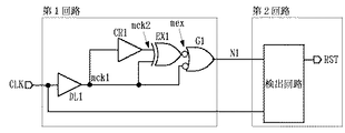
図1には、この発明に係るクロック周波数検出回路を備えた半導体集積回路装置の一実施例のブロック図が示されている。この実施例の半導体集積回路装置は、第1回路と第2回路から構成される。第1回路は、クロック周波数の検出を行う以下の回路より構成される。クロックCLKは、遅延回路DL1を通して遅延されて周波数検出を行うCR遅延回路CR1に入力される。この実施例のCR遅延回路CR1は、上記遅延回路DL1の遅延信号nck1の周波数が所定の周波数よりも低いときにはクロックnck1(CLK)に対応した周波数のパルスを出力し、上記遅延信号nck1の周波数が所定の周波数よりも高いときにはロウレベル又はハイレベルのような固定電位を出力する。 FIG. 1 is a block diagram showing an embodiment of a semiconductor integrated circuit device provided with a clock frequency detection circuit according to the present invention. The semiconductor integrated circuit device of this embodiment is composed of a first circuit and a second circuit. The first circuit includes the following circuits that detect the clock frequency. The clock CLK is delayed through the delay circuit DL1 and input to the CR delay circuit CR1 that performs frequency detection. The CR delay circuit CR1 of this embodiment outputs a pulse having a frequency corresponding to the clock nck1 (CLK) when the frequency of the delay signal nck1 of the delay circuit DL1 is lower than a predetermined frequency, and the frequency of the delay signal nck1 is When the frequency is higher than a predetermined frequency, a fixed potential such as a low level or a high level is output.
この実施例では、クロックCLKの周波数が所定の周波数よりも低いときと高いときのいずれにおいてもパルス信号の形態の周波数検出信号を出力するように、排他的論理和回路EX1及びゲート回路Gが設けられる。つまり、上記CR遅延回路CR1の出力信号nck2は、排他的論理和回路EX1の一方の入力に供給される。この排他的論理和回路EX1の他方の入力には、上記遅延信号nck1が供給される。この排他的論理和回路EX1の出力信号と、上記遅延信号nck1とはゲート回路G1を通して論理和信号が検出信号N1として出力される。 In this embodiment, the exclusive OR circuit EX1 and the gate circuit G are provided so as to output a frequency detection signal in the form of a pulse signal regardless of whether the frequency of the clock CLK is lower or higher than a predetermined frequency. It is done. That is, the output signal nck2 of the CR delay circuit CR1 is supplied to one input of the exclusive OR circuit EX1. The delay signal nck1 is supplied to the other input of the exclusive OR circuit EX1. The output signal of the exclusive OR circuit EX1 and the delayed signal nck1 are output as a detection signal N1 through the gate circuit G1.
上記検出信号N1は、上記のようにクロックCLKの周波数が所定の周波数よりも低いときと高いときのいずれにおいてもパルス信号の形態とされるものであるので、その識別のために上記クロックCLKとともに第2回路に含まれる検出回路に伝えられる。この検出回路では、上記クロックCLKを用いて上記パルス信号の形態の検出信号N1を解読する。つまり、クロックCLKの周波数が所定の周波数よりも低いときには低周波クロック検出信号を含むリセット信号RSTを発生させ、クロックCLKの周波数が所定の周波数よりも高いときにはリセット信号RSTを発生させない。この結果、第2回路に含まれる図示しない信号処理回路では、リセット信号RSTが無効の状態では内部回路がクロックCLKに対応した所定の信号処理動作を行い、リセット信号RSTが有効とされると信号処理回路の動作が強制的に停止させられあるいは無効にさせられる。 Since the detection signal N1 is in the form of a pulse signal both when the frequency of the clock CLK is lower and higher than the predetermined frequency as described above, it is used together with the clock CLK for identification. The signal is transmitted to a detection circuit included in the second circuit. In this detection circuit, the detection signal N1 in the form of the pulse signal is decoded using the clock CLK. That is, the reset signal RST including the low frequency clock detection signal is generated when the frequency of the clock CLK is lower than the predetermined frequency, and the reset signal RST is not generated when the frequency of the clock CLK is higher than the predetermined frequency. As a result, in a signal processing circuit (not shown) included in the second circuit, when the reset signal RST is invalid, the internal circuit performs a predetermined signal processing operation corresponding to the clock CLK, and the signal is output when the reset signal RST is validated. The operation of the processing circuit is forcibly stopped or disabled.
図2には、図1のCR遅延回路の一実施例の回路図が示されている。同図には、参考として図1に用いられた回路記号とそれに対応した具体的回路が示されている。抵抗RとキャパシタCとが直列形態に接続される。上記キャパシタCには、PチャネルMOSFETQ2から上記抵抗Rを通して電源端子VDDから充電電流が供給される。また、上記キャパシタCには、それと並列形態に接続されたNチャネルMOSFETQ1により構成された放電経路が設けられる。上記MOSFETQ1のソースは、回路の接地電位VSSに接続され、上記キャパシタCは回路の接地電位VSSを基準にして上記充電動作及び放電動作が行われる。上記キャパシタCの電圧は、インバータ回路IV2の入力端子に供給される。このインバータ回路IV2は、そのロジックスレショルド電圧を参照電圧として上記キャパシタCの電圧判定を行う。 FIG. 2 shows a circuit diagram of an embodiment of the CR delay circuit of FIG. In the figure, the circuit symbols used in FIG. 1 and specific circuits corresponding thereto are shown for reference. A resistor R and a capacitor C are connected in series. Charging current is supplied from the power supply terminal VDD to the capacitor C through the resistor R from the P-channel MOSFET Q2. The capacitor C is provided with a discharge path constituted by an N-channel MOSFET Q1 connected in parallel with the capacitor C. The source of the MOSFET Q1 is connected to the circuit ground potential VSS, and the capacitor C performs the charging and discharging operations with reference to the circuit ground potential VSS. The voltage of the capacitor C is supplied to the input terminal of the inverter circuit IV2. The inverter circuit IV2 determines the voltage of the capacitor C using the logic threshold voltage as a reference voltage.
この実施例のCR遅延回路は、入力端子inに供給されるパルスの周波数が低いときには、それがロウレベルの期間にPチャネルMOSFETQ2がオン状態となり、抵抗Rを介してキャパシタCに充電動作が行われる。このときの時定数に従ってキャパシタCにはチャージアップが行われる。このチャージアップ動作によって、インバータ回路IV2の入力電圧がそのロジックスレッショルド電圧を越えると、インバータ回路IV2の出力信号outはハイレベルからロウレベルに変化する。 In the CR delay circuit of this embodiment, when the frequency of the pulse supplied to the input terminal in is low, the P-channel MOSFET Q2 is turned on during the low level period, and the capacitor C is charged via the resistor R. . The capacitor C is charged up according to the time constant at this time. When the input voltage of the inverter circuit IV2 exceeds the logic threshold voltage by this charge-up operation, the output signal out of the inverter circuit IV2 changes from high level to low level.
入力端子inに供給されるパルスがハイレベルに変化すると、PチャネルMOSFETQ2がオフ状態になり、NチャネルMOSFETQ1がオン状態となるのでキャパシタCの放電動作を行う。この放電動作によって、キャパシタCの電圧が低下し、インバータ回路IV2の入力電圧がそのロジックスレッショルド電圧より低下すると、インバータ回路IV2の出力信号outはロウレベルからハイレベルに変化する。このように、キャパシタCの電圧が上記インバータ回路IV2のロジックスレッショルド電圧を越えるような低い周波数のときには、入力端子inに供給されるパルスに対応した周波数のパルスが出力される。 When the pulse supplied to the input terminal in changes to high level, the P-channel MOSFET Q2 is turned off and the N-channel MOSFET Q1 is turned on, so that the capacitor C is discharged. As a result of this discharging operation, when the voltage of the capacitor C decreases and the input voltage of the inverter circuit IV2 decreases below its logic threshold voltage, the output signal out of the inverter circuit IV2 changes from low level to high level. As described above, when the voltage of the capacitor C has a low frequency exceeding the logic threshold voltage of the inverter circuit IV2, a pulse having a frequency corresponding to the pulse supplied to the input terminal in is output.
入力端子inに供給されるパルスの周波数が高くなり、それがロウレベルの期間に上記PチャネルMOSFETQ2がオン状態となり、抵抗Rを介してキャパシタCに充電動作が行われてキャパシタCの電圧は上記時定数に従って上昇するが、インバータ回路IV2のロジックスレッショルド電圧に到達する前に、上記ロウレベル期間からハイレベルに期間に切り替わり、PチャネルMOSFETQ2がオフ状態になり、NチャネルMOSFETQ1がオン状態となるのでキャパシタCの放電動作を行う。この結果、インバータ回路IV2の入力電圧がそのロジックスレショルド電圧に到達しないから定常的にハイレベルの出力信号を形成するものとなる。 The frequency of the pulse supplied to the input terminal “in” becomes high, the P-channel MOSFET Q2 is turned on during the low level period, the capacitor C is charged through the resistor R, and the voltage of the capacitor C is The voltage rises according to a constant, but before reaching the logic threshold voltage of the inverter circuit IV2, the low-level period is switched to the high level period, the P-channel MOSFET Q2 is turned off, and the N-channel MOSFET Q1 is turned on. The discharge operation is performed. As a result, since the input voltage of the inverter circuit IV2 does not reach the logic threshold voltage, a high level output signal is steadily formed.
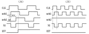
図3には、図1のクロック周波数検出回路の動作の一例を説明するためのタイミング図が示されている。図3(A)は、クロックCLKの周波数が低いときのタイミング図であり、図3(B)は、クロックCLKの周波数が高いときのタイミング図である。図3(A)において、クロックCLKに対して遅延クロックnck1は、遅延回路DL1の遅延時間tdだけ遅延される。CR遅延回路CR1の出力信号nck2は、前記のように周波数が低いのでその時定数に対応した遅延時間tcrだけ遅延させられる。図2のようなCR時定数回路を用いた場合には、周波数に対応してパルス幅(パルスデューティ)が遅延信号nck1に対して狭くなる周波数領域もあるが、同図ではそれよりクロックCLKの周波数が低い場合を例にしている。 FIG. 3 is a timing chart for explaining an example of the operation of the clock frequency detection circuit of FIG. FIG. 3A is a timing diagram when the frequency of the clock CLK is low, and FIG. 3B is a timing diagram when the frequency of the clock CLK is high. In FIG. 3A, the delay clock nck1 is delayed from the clock CLK by the delay time td of the delay circuit DL1. Since the output signal nck2 of the CR delay circuit CR1 has a low frequency as described above, it is delayed by the delay time tcr corresponding to the time constant. When the CR time constant circuit as shown in FIG. 2 is used, there is a frequency region in which the pulse width (pulse duty) becomes narrower than the delay signal nck1 corresponding to the frequency. The case where the frequency is low is taken as an example.
排他的論理和回路EX1は、上記2つのパルスnck1とnck2のレベルが一致したときにロウレベル、不一致のときにハイレベルの出力信号nexを形成する。この信号nexと上記クロックnck1とをゲート回路Gで論理を採ること、具体的にはクロックnck1がハイレベルのときの信号nexの一致出力であるロウレベルをノードN1から出力させる。言い換えると、クロックnck1がロウレベルのときにはゲート回路G1のゲートを閉じて信号nexに無関係にノードN1をハイレベルにする。 The exclusive OR circuit EX1 forms a low level output signal nex when the levels of the two pulses nck1 and nck2 match, and a high level output signal nex when they do not match. The logic of the signal nex and the clock nck1 is taken by the gate circuit G. Specifically, a low level that is a coincident output of the signal nex when the clock nck1 is at a high level is output from the node N1. In other words, when the clock nck1 is at low level, the gate of the gate circuit G1 is closed and the node N1 is set to high level regardless of the signal nex.
このようにして、クロックCLKの周波数が低いときには、上記ノードN1が上記クロックnck1の周期に対応してロウレベルになる期間が発生する。このようなノードN1のパルス信号は、検出回路に伝えられる。検出回路は、クロックCLKのエッジを用いてノードN1のロウレベル/ハイレベルの判定が行われる。同図では、クロックCLKの立ち下がりエッジで最初に上記ノードN1のハイレベルを検出すると、リセット信号RSTを発生させる。このリセット信号RSTはラッチ回路等により保持される。 In this way, when the frequency of the clock CLK is low, a period in which the node N1 is at a low level corresponding to the cycle of the clock nck1 occurs. Such a pulse signal of the node N1 is transmitted to the detection circuit. The detection circuit determines the low level / high level of the node N1 using the edge of the clock CLK. In the figure, when the high level of the node N1 is first detected at the falling edge of the clock CLK, the reset signal RST is generated. This reset signal RST is held by a latch circuit or the like.
図3(B)において、クロックCLKに対して遅延クロックnck1は、遅延回路DL1の遅延時間tdだけ遅延される。CR遅延回路CR1の出力信号nck2は、前記のように周波数が高いのでハイレベルのような固定レベルにされる。排他的論理和回路EX1は、上記2つのパルスnck1とnck2のレベルが一致したときにロウレベル、不一致のときにハイレベルの出力信号nexを形成する。したがって、上記のようにnck2のレベルがハイレベルであるので、上記クロックnck1を反転させた信号をノードN1から出力させる。 In FIG. 3B, the delay clock nck1 is delayed by the delay time td of the delay circuit DL1 with respect to the clock CLK. Since the output signal nck2 of the CR delay circuit CR1 has a high frequency as described above, it is set to a fixed level such as a high level. The exclusive OR circuit EX1 forms a low level output signal nex when the levels of the two pulses nck1 and nck2 match, and a high level output signal nex when they do not match. Accordingly, since the level of nck2 is high as described above, a signal obtained by inverting the clock nck1 is output from the node N1.
このようにして、クロックCLKの周波数が高いときにも、上記ノードN1が上記クロックnck1に対応したパルス信号とされる。このようなノードN1のパルス信号は、検出回路に伝えられる。検出回路は、クロックCLKのエッジを用いてロウレベル/ハイレベルの判定が行う。同図では、クロックCLKの立ち上がりエッジで上記ノードN1のハイレベル/立ち下がりエッジで上記ノードN1のロウレベルを検出するとリセット信号RSTを発生させない。このようなレベル判定のために遅延回路DL1が設けられており、ここでの遅延時間tdが上記ノードN1のハイレベル/ロウレベルを取り込むためのセットアップ時間とされる。 Thus, even when the frequency of the clock CLK is high, the node N1 is a pulse signal corresponding to the clock nck1. Such a pulse signal of the node N1 is transmitted to the detection circuit. The detection circuit performs the low level / high level determination using the edge of the clock CLK. In the figure, when the low level of the node N1 is detected at the high level / falling edge of the node N1 at the rising edge of the clock CLK, the reset signal RST is not generated. A delay circuit DL1 is provided for such level determination, and the delay time td here is set as a setup time for taking in the high level / low level of the node N1.
図1の検出回路の真理値表1は、次の通りである。 The truth table 1 of the detection circuit of FIG. 1 is as follows.
真理知表1
┌───┬────┬─────┐
│CLK│N1 │RST │
├───┼────┼─────┤
│↑ │0 │ 1 │
│↑ │1 │ 0 │
│↓ │0 │ 0 │
│↓ │1 │ 1 │
└───┴────┴─────┘
↑は立ち上がりエッジ
↓は立ち下がりエッジ
0はロウレベル(論理0)
1はハイレベル(論理1)
Truth Table 1
┌───┬────┬─────┐
│CLK│N1 │RST │
├───┼────┼─────┤
│ ↑ │0 │ 1 │
│ ↑ │1 │ 0 │
│ ↓ │0 │ 0 │
│ ↓ │1 │ 1 │
└───┴────┴─────┘
↑ is rising edge ↓ is falling
1 is high level (logic 1)
なお、上記遅延回路DL1は、省略できるものである。すなわち、ノードN1の信号は、上記のようなゲート回路G1によって遅延されるので、ここでの遅延時間を利用して上記検出回路でのノードN1のハイレベル/ロウレベルを取り込むためのセットアップ時間に利用することができる。あるいは、検出回路側でかかるセットアップを設定する遅延回路等を設ける構成であってもよい。 Note that the delay circuit DL1 can be omitted. That is, since the signal of the node N1 is delayed by the gate circuit G1 as described above, the delay time here is used for the setup time for taking in the high level / low level of the node N1 in the detection circuit. can do. Or the structure which provides the delay circuit etc. which set this setup by the detection circuit side may be sufficient.
上記のようにクロックCLKの周波数が検出閾値(検出周波数)よりも高い場合は、クロックCLKそのもの(図1の回路では遅延信号nck1)が反転されてノードN1から出力される。クロックCLK周波数が検出閾値(検出周波数)より低い場合は、CR遅延回路CR1により遅延される。この遅延信号nck2が排他的論理和回路EX1及びゲート回路G1を通すことでノードN1はクロックCLKの次のエッジの前にハイレベル(H)になる。 As described above, when the frequency of the clock CLK is higher than the detection threshold (detection frequency), the clock CLK itself (the delayed signal nck1 in the circuit of FIG. 1) is inverted and output from the node N1. When the clock CLK frequency is lower than the detection threshold (detection frequency), it is delayed by the CR delay circuit CR1. The delayed signal nck2 passes through the exclusive OR circuit EX1 and the gate circuit G1, so that the node N1 becomes high level (H) before the next edge of the clock CLK.
つまり、クロックCLK周波数が検出閾値(検出周波数)より低い場合は、クロックCLKのエッジでは必ずHを出す。これを前記真理値表1のような検出回路を用いることにより、クロックCLKのネガティブエッジのときにリセット信号RSTがハイレベル(H)になり図示しない信号処理回路をリセット状態にする。非検出時にはノードN1がクロックnck1に対応して交流化される。もしも、かかる信号経路であるノードN1をハイレベル/ロウレベルのいずれかに強制的に固定すると必ずリセット信号RSTがハイレベル(H)になり、リセットがかかるようになる。 That is, when the clock CLK frequency is lower than the detection threshold (detection frequency), H is always output at the edge of the clock CLK. By using this detection circuit as shown in the truth table 1, the reset signal RST becomes a high level (H) at the negative edge of the clock CLK, and the signal processing circuit (not shown) is reset. At the time of non-detection, the node N1 is ACed corresponding to the clock nck1. If the node N1, which is such a signal path, is forcibly fixed to either the high level or the low level, the reset signal RST always becomes the high level (H), and the reset is started.
この実施例のように検出回路に至る信号経路(ノードN1)の信号のうちの固定レベル(直流的信号)を上記のような排他的論理和回路及びゲート回路G1を組み合わせることでパルス信号(交流的信号)にする回路構成にしたことで、CR遅延回路CR1で形成される検出信号のうちの直流的信号が見えないようにした。この結果、低周波数検出回路を有するICにおいて、低周波数検出回路に供給されるクロックCLKが所定周波数範囲内にあるときと、所定周波数範囲外にある時で異なるパターンのパルス信号(交流信号)を出力する第1回路と、かかる第1回路の出力とクロックCLK(上記とは別でも可)とにより上記出力を取りこむ第2回路を設けることにより、外部からの不正アタックに対する内部情報の機密を保持することができる。 As in this embodiment, a fixed level (DC signal) of the signals on the signal path (node N1) leading to the detection circuit is combined with the exclusive OR circuit and the gate circuit G1 as described above to generate a pulse signal (AC Circuit), the DC signal among the detection signals formed by the CR delay circuit CR1 is made invisible. As a result, in an IC having a low frequency detection circuit, pulse signals (AC signals) having different patterns are generated when the clock CLK supplied to the low frequency detection circuit is within a predetermined frequency range and when the clock CLK is outside the predetermined frequency range. Maintaining confidentiality of internal information against illegal attacks from the outside by providing a first circuit that outputs and a second circuit that captures the output by the output of the first circuit and the clock CLK (may be different from the above) can do.
すなわち、ノードN1にクロックCLKが重畳した信号を検出回路への出力とすることで、低周波検出での完全交流信号化が可能となり、その信号伝達経路の特定が困難となるばかりか、外部からノードN1に対して固定レベルを供給するような攻撃を受けた場合でも、リセット信号RSTを出すので内部情報を取り出しの防止をすることができる。この結果、外部攻撃に対するICチップのセキュリティが向上することでセキュリティ認証を取得しやすくなり、ICカード用マイコンとしての付加価値を高める事ができる。 That is, by making a signal with the clock CLK superimposed on the node N1 as an output to the detection circuit, it becomes possible to make a complete AC signal with low frequency detection, and it becomes difficult to specify the signal transmission path from the outside. Even in the case of an attack that supplies a fixed level to the node N1, the reset signal RST is issued, so that internal information can be prevented from being taken out. As a result, the security of the IC chip against external attacks is improved, so that it is easy to obtain security authentication, and the added value as an IC card microcomputer can be increased.
CR時定数回路のようなアナログディレイ素子の出力信号を前記のような排他的論理和回路及びゲート回路で交流信号化することで、ディレイ時間の高精度化と高セキュリティ化を両立できる。低周波数検出回路はIC内部のマイクロプロセッサやマイクロコンピュータ等の動作周波数以外の周波数入力を禁止し、誤動作を防ぐために必須の回路である。よって、この周波数回路の閥値が使用条件でばらついたりすることは望ましくない。結果として、CR時定数回路のようなアナログ素子を使用したディレイ回路を使用するのが望ましい。 By converting the output signal of an analog delay element such as a CR time constant circuit into an AC signal by the exclusive OR circuit and the gate circuit as described above, both high accuracy of delay time and high security can be achieved. The low frequency detection circuit is an indispensable circuit for prohibiting frequency input other than the operating frequency of the microprocessor or microcomputer in the IC and preventing malfunction. Therefore, it is not desirable that the threshold value of the frequency circuit varies depending on use conditions. As a result, it is desirable to use a delay circuit using analog elements such as a CR time constant circuit.
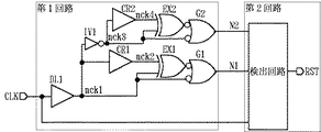
図4には、この発明に係るクロック周波数検出回路を備えた半導体集積回路装置の他の一実施例のブロック図が示されている。この実施例では、図1の第1回路の低周波数を検出するための回路が2組設けられる。つまり、前記図1と同様なCR遅延回路CR1、排他的論理和回路EX1及びゲート回路G1からなる低周波数検出部と、それと同じ回路構成からなるCR遅延回路CR2,排他的論理和回路EX2及びゲート回路G2が設けられる。そして、この新たに設けられたCR遅延回路CR2及び排他的論理和回路EX2には、上記遅延信号nck1の反転信号nck3が供給される。この反転信号nck3は、上記遅延信号nck1を受けるインバータ回路IV1によって形成される。これら2組の低周波数を検出するための回路によりそれぞれ検出信号N1とN2が形成されて、第2回路に含まれる検出回路に伝えられる。 FIG. 4 is a block diagram showing another embodiment of a semiconductor integrated circuit device having a clock frequency detection circuit according to the present invention. In this embodiment, two sets of circuits for detecting the low frequency of the first circuit of FIG. 1 are provided. That is, the low frequency detection unit including the CR delay circuit CR1, the exclusive OR circuit EX1, and the gate circuit G1 as in FIG. 1, the CR delay circuit CR2, the exclusive OR circuit EX2, and the gate having the same circuit configuration as the low frequency detection unit. A circuit G2 is provided. The newly provided CR delay circuit CR2 and exclusive OR circuit EX2 are supplied with the inverted signal nck3 of the delay signal nck1. This inverted signal nck3 is formed by an inverter circuit IV1 that receives the delay signal nck1. Detection signals N1 and N2 are formed by the circuits for detecting these two sets of low frequencies, respectively, and transmitted to the detection circuit included in the second circuit.
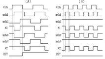
図5には、図4のクロック周波数検出回路の動作の一例を説明するためのタイミング図が示されている。この実施例では、上記新たに設けられた周波数検出部によりクロックCLKがロウレベルの期間において、上記排他的論理和回路EX2の不一致出力に対応したロウレベルのパルスがノードN2から出力される。このように排他的論理和回路EX1とEX2をパラレルに配置することにより、図1の実施例の回路と比較して、クロックCLKのポジティブエッジ及びネガティエッジの両方のエッジで低周波の検出が可能となり、よりセキュリティ性を向上させることができる。例えば、クロックCLKのパルスデューティを変更することにより行われる不正アタックを防ぐことができる。 FIG. 5 is a timing chart for explaining an example of the operation of the clock frequency detection circuit of FIG. In this embodiment, a low level pulse corresponding to the mismatch output of the exclusive OR circuit EX2 is output from the node N2 during the period when the clock CLK is low level by the newly provided frequency detection unit. In this way, by arranging the exclusive OR circuits EX1 and EX2 in parallel, it is possible to detect low frequency at both the positive edge and the negative edge of the clock CLK as compared with the circuit of the embodiment of FIG. Thus, security can be further improved. For example, an illegal attack performed by changing the pulse duty of the clock CLK can be prevented.
図6には、この発明に係るクロック周波数検出回路を備えた半導体集積回路装置の更に他の一実施例のブロック図が示されている。この実施例では、図4の第1回路の排他的論理和回路EX1,EX2をオアゲート回路G3及びG4に置き換えたものであり、あるいは排他的論理和回路EX1,EX2を省略してゲート回路G1,G2を上記オアゲート回路G3及びG4に置き換えたものである。このようなオアゲート回路G3,G4を用いて検出論理を変えての構成も可能である。 FIG. 6 is a block diagram showing still another embodiment of a semiconductor integrated circuit device having a clock frequency detection circuit according to the present invention. In this embodiment, the exclusive OR circuits EX1 and EX2 of the first circuit of FIG. 4 are replaced with OR gate circuits G3 and G4, or the exclusive OR circuits EX1 and EX2 are omitted and the gate circuits G1 and EX2 are omitted. G2 is replaced with the above OR gate circuits G3 and G4. A configuration in which the detection logic is changed using such OR gate circuits G3 and G4 is also possible.
図7には、図6のクロック周波数検出回路の動作の一例を説明するためのタイミング図が示されている。上記のようなオアゲート回路G3,G4を用いることにより、ノードN1,N2のパルスは、前記図4の実施例と同様なパルスとすることができる。このように排他的論理和回路をオアゲート回路に変えても前記図4と同様の検出が可能となる。 FIG. 7 is a timing chart for explaining an example of the operation of the clock frequency detection circuit of FIG. By using the OR gate circuits G3 and G4 as described above, the pulses at the nodes N1 and N2 can be the same as those in the embodiment of FIG. Thus, even if the exclusive OR circuit is changed to an OR gate circuit, the same detection as in FIG. 4 is possible.
前記図4及び図6の検出回路の真理値表2は、次の通りである。 The truth table 2 of the detection circuit of FIGS. 4 and 6 is as follows.
真理知表2
┌───┬───┬───┬───┐
│CLK│N1 │N2 │RST│
├───┼───┼───┼───┤
│↑ │0 │0 │1 │
│↑ │1 │1 │1 │
│↓ │0 │0 │1 │
│↓ │1 │1 │1 │
├───┼───┼───┼───┤
│↑ │0 │1 │1 │
│↑ │1 │0 │0 │
│↓ │0 │1 │0 │
│↓ │1 │0 │1 │
└───┴───┴───┴───┘
↑は立ち上がりエッジ
↓は立ち下がりエッジ
0はロウレベル(論理0)
1はハイレベル(論理1)
Truth Table 2
┌───┬───┬───┬───┐
│CLK│N1 │N2 │RST│
├───┼───┼───┼───┤
│ ↑ │0 │0 │1 │
│ ↑ │1 │1 │1 │
│ ↓ │0 │0 │1 │
│ ↓ │1 │1 │1 │
├───┼───┼───┼───┤
│ ↑ │0 │1 │1 │
│ ↑ │1 │0 │0 │
│ ↓ │0 │1 │0 │
│ ↓ │1 │0 │1 │
└───┴───┴───┴───┘
↑ is rising edge ↓ is falling
1 is high level (logic 1)
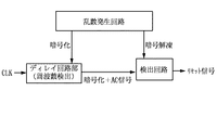
図8には、この発明に係るクロック周波数検出回路を備えた半導体集積回路装置の更に他の一実施例のブロック図が示されている。この実施例では、半導体集積回路装置に乱数発生回路を搭載して、第1回路に対応したディレイ回路部に暗号化を入力し、前記AC信号+暗号化を形成して第2回路の検出回路に伝達する。そして、検出回路では上記乱数発生回路から供給される暗号解凍を受けて上記第1回路から伝えられるAC信号+暗号化の中からAC信号を取り出してリセット信号を発生させる。これにより、ノードN1に出力される信号をAC信号化+暗号化することで、AC信号自体を解析することを困難としてセキュリティ性を向上させることができる。例えば、ICカード搭載用の半導体集積回路装置は乱数発生回路を備えているものがあり、かかる半導体集積回路装置では乱数発生回路を共用することができる。 FIG. 8 is a block diagram showing still another embodiment of a semiconductor integrated circuit device having a clock frequency detection circuit according to the present invention. In this embodiment, a random number generation circuit is mounted on a semiconductor integrated circuit device, encryption is input to a delay circuit section corresponding to the first circuit, and the AC signal + encryption is formed to detect the second circuit. To communicate. The detection circuit receives the encryption decompression supplied from the random number generation circuit, extracts the AC signal from the AC signal + encryption transmitted from the first circuit, and generates a reset signal. Thus, by converting the signal output to the node N1 into an AC signal and encrypting it, it is difficult to analyze the AC signal itself, and security can be improved. For example, some semiconductor integrated circuit devices for mounting an IC card include a random number generation circuit, and such a semiconductor integrated circuit device can share the random number generation circuit.
図9には、図8のクロック周波数検出回路の一実施例の具体的ブロック図が示されている。乱数発生回路で形成された乱数信号をパルス列として出力し、それを排他的論理和回路EX3とEX4に供給する。上記排他的論理和回路EX3の他方の入力には、上記図1、図4あるいは図4の実施例のようなディレイ回路部(周波数検出)の出力信号N1を供給する。排他的論理和信号EX3は、上記パルス列からなる乱数が論理1のときには、上記ノードN1の出力レベルを反転させ、乱数が論理0のときには上記ノードN1の出力信号をそのまま出力するという乱数信号を発生させる。検出回路側に設けられた排他的論理和回路EX4は、上記同じパルス列からなる乱数が論理1のときには、上記AC信号のレベルを反転させ、乱数が論理0のときには上記AC信号をそのまま出力する。このようにして、検出回路には上記ノードN1に対応したAC信号のみが再生されて伝えられる。
FIG. 9 shows a specific block diagram of an embodiment of the clock frequency detection circuit of FIG. The random number signal formed by the random number generation circuit is output as a pulse train and supplied to the exclusive OR circuits EX3 and EX4. The other input of the exclusive OR circuit EX3 is supplied with the output signal N1 of the delay circuit section (frequency detection) as in the embodiment of FIG. 1, FIG. 4 or FIG. The exclusive OR signal EX3 generates a random number signal that inverts the output level of the node N1 when the random number of the pulse train is logic 1, and outputs the output signal of the node N1 as it is when the random number is
特に制限されないが、排他的論理和回路EX3のノードN1がアナログ部のウエルとデジタル部のウエルにまたがって存在して、2つの排他的論理和回路EX3,EX4とそれらを結ぶ配線についてノードN1以外がデジタル部のウエルに存在している。このような構成にすると2つの排他的論理和回路EX3,EX4やそれらを結ぶ配線がアナログ部のウエルとデジタル部のウエルにまたがっていたら、配線が見つけられてパターン解析されてしまうことを防ぐ上で有益となる。 Although not particularly limited, the node N1 of the exclusive OR circuit EX3 exists across the well of the analog part and the well of the digital part, and the two exclusive OR circuits EX3 and EX4 and the wiring connecting them are other than the node N1. Is present in the well of the digital part. With such a configuration, if the two exclusive OR circuits EX3 and EX4 and the wiring connecting them extend over the analog well and the digital well, the wiring is found and the pattern analysis is prevented. It will be beneficial.
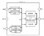
図10には、この発明に係る半導体集積回路装置が搭載されたICカードの一実施例のブロック図が示されている。この実施例では、演算回路、ROM(リード・オンリー・メモリ)、RAM(ランダム・アクセス・メモリ)、FLASH(一括消去型不揮発性メモリ)のような各種メモリ、周辺回路からなる信号処理回路に、上記半導体集積回路装置の動作に必要な電源を供給するための第1電源端子と該第一電源端子よりも低い電源を供給するための第2電源端子と、上記半導体集積回路装置の内部回路をリセットするためのリセット端子と、上記第1クロックが供給されるクロック端子と、上記半導体集積回路装置の外部との信号入出力を行うための入出力端子と、保護回路として前記説明したような低周波数検出回路(LFD)の他に、高周波数検出回路(HFD)、低電圧検出回路(LVD)、高電圧検出回路(HVD)が設けられる。これらの各検出回路で検出信号が形成されると、リセット信号RSTが形成されて上記信号処理回路を構成する演算回路、ROM、RAM、FLASHのような各種メモリ、周辺回路の動作が強制的に停止(リセット)状態にされる。 FIG. 10 is a block diagram showing an embodiment of an IC card on which the semiconductor integrated circuit device according to the present invention is mounted. In this embodiment, a signal processing circuit including an arithmetic circuit, a ROM (Read Only Memory), a RAM (Random Access Memory), a FLASH (Batch Erase Nonvolatile Memory), a peripheral circuit, A first power supply terminal for supplying power necessary for the operation of the semiconductor integrated circuit device; a second power supply terminal for supplying power lower than the first power supply terminal; and an internal circuit of the semiconductor integrated circuit device. A reset terminal for resetting, a clock terminal to which the first clock is supplied, an input / output terminal for inputting / outputting a signal to / from the outside of the semiconductor integrated circuit device, and a protection circuit as described above In addition to the frequency detection circuit (LFD), a high frequency detection circuit (HFD), a low voltage detection circuit (LVD), and a high voltage detection circuit (HVD) are provided. When a detection signal is formed by each of these detection circuits, a reset signal RST is formed to force the operation of various arithmetic circuits, ROM, RAM, FLASH, and peripheral circuits constituting the signal processing circuit. Stopped (reset) state.
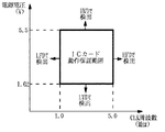
図11には、この発明が適用されるICカードの動作特性図が示されている。この実施例のICカードは、動作周波数としては低周波数検出回路(LFD)で設定された周波数よりも高い領域でかつ高周波数検出回路(HFD)で設定された周波数よりも低い領域が動作補償範囲とされ、動作電圧としては低電圧検出回路(LVD)で設定された電圧よりも高い領域でかつ高電圧検出回路(HVD)で設定された電圧よりも低い領域が動作補償範囲とされる。このようなICカードの動作補償範囲以外の周波数のクロックが端子CLKから供給されたり、ICカードの動作補償範囲以外の電圧が電源端子から供給されたりすると、これらの回路が検知して、上記信号処理回路を構成する演算回路、ROM、RAM、FLASHのような各種メモリ、周辺回路の動作が強制的に停止(リセット)状態にされる。 FIG. 11 shows an operating characteristic diagram of an IC card to which the present invention is applied. The IC card of this embodiment has an operation compensation range in which the operating frequency is higher than the frequency set by the low frequency detection circuit (LFD) and lower than the frequency set by the high frequency detection circuit (HFD). As the operation voltage, the region that is higher than the voltage set by the low voltage detection circuit (LVD) and lower than the voltage set by the high voltage detection circuit (HVD) is set as the operation compensation range. When such a clock having a frequency outside the operation compensation range of the IC card is supplied from the terminal CLK, or when a voltage outside the operation compensation range of the IC card is supplied from the power supply terminal, these circuits detect the above signal. The operations of the arithmetic circuit, the various memories such as ROM, RAM, and FLASH, and the peripheral circuits constituting the processing circuit are forcibly stopped (reset).
以上本発明者によってなされた発明を、前記実施形態に基づき具体的に説明したが、本発明は、前記実施形態に限定されるものではなく、その要旨を逸脱しない範囲において種々変更可能である。例えば、上記のように周波数検出信号のうちの固定レベルにされる信号に対してクロックを用いてパルス信号に変換する回路は、種々の実施形態を採ることができる。上記CR遅延回路は、キャパシタと抵抗とを並列形態に接続して、例えばPチャネルMOSFETにより充電電流を供給し、放電経路は並列接続の抵抗により行うようにするものであってもよい。このように遅延回路によって所定の周波数を検出する回路は、種々の実施形態を採ることができるものである。この発明は、周波数検出により内部回路の保護機能の強化を実現した半導体集積回路装置に広く利用できる。 Although the invention made by the inventor has been specifically described based on the above embodiment, the present invention is not limited to the above embodiment, and various modifications can be made without departing from the scope of the invention. For example, as described above, a circuit that converts a signal having a fixed level among frequency detection signals into a pulse signal using a clock can take various embodiments. The CR delay circuit may be configured such that a capacitor and a resistor are connected in parallel, a charging current is supplied by, for example, a P-channel MOSFET, and a discharging path is performed by a resistor connected in parallel. As described above, the circuit for detecting the predetermined frequency by the delay circuit can take various embodiments. The present invention can be widely used for semiconductor integrated circuit devices in which the protection function of the internal circuit is enhanced by frequency detection.
DL…遅延回路、CR1,CR2…CR遅延回路(周波数検出)、EX1〜EX4…排他的論理和回路、G1〜G4…ゲート回路、IV1,IV2…インバータ回路、Q1,Q2…MOSFET、R…抵抗、C…キャパシタ。 DL ... delay circuit, CR1, CR2 ... CR delay circuit (frequency detection), EX1 to EX4 ... exclusive OR circuit, G1 to G4 ... gate circuit, IV1, IV2 ... inverter circuit, Q1, Q2 ... MOSFET, R ... resistance , C: Capacitor.
Claims (10)
上記低周波クロック検出回路は、第1回路と第2回路を有し、
上記第1回路は、第1クロックが供給され、上記一定の周波数よりも低い時と上記一定の周波数よりも高い時とのそれぞれにおいて上記第1クロックを基準にして異なる波形とみなされる第1信号を出力し、
上記第2回路は、上記第1信号と上記第1クロックに基づいて上記低周波クロック検出信号を出力することを特徴とする半導体集積回路装置。 It has a low-frequency clock detection circuit that detects whether the frequency is lower than a certain frequency, and the operation of the internal circuit is forcibly stopped or invalidated based on the low-frequency clock detection signal formed by the low-frequency clock circuit. A semiconductor integrated circuit device comprising:
The low frequency clock detection circuit has a first circuit and a second circuit,
The first circuit is supplied with a first clock, and is considered to have a different waveform with respect to the first clock when the frequency is lower than the fixed frequency and when the frequency is higher than the fixed frequency. Output
The semiconductor integrated circuit device, wherein the second circuit outputs the low-frequency clock detection signal based on the first signal and the first clock.
上記第2回路は、上記第1信号と第1クロックに基づいて上記第1クロックが上記一定の周波数よりも低いと判定される条件が成立すると、その状態を保持して上記低周波クロック検出信号を出力することを特徴とする半導体集積回路装置。 In claim 1,
When the condition for determining that the first clock is lower than the fixed frequency is satisfied based on the first signal and the first clock, the second circuit maintains the state and maintains the low frequency clock detection signal. Output a semiconductor integrated circuit device.
上記第1信号は、上記第1クロックが上記一定の周波数よりも低い時と上記一定の周波数よりも高い時とのそれぞれにおいて周期が異なるものであることを特徴とする半導体集積回路装置。 In claim 1,
The semiconductor integrated circuit device according to claim 1, wherein the first signal has a different period when the first clock is lower than the fixed frequency and when the first clock is higher than the fixed frequency.
上記第1信号は、上記第1クロックが上記一定の周波数よりも低い時と上記一定の周波数よりも高い時とのそれぞれにおいてパルスデューティが異なるものであることを特徴とする半導体集積回路装置。 In claim 1,
The semiconductor integrated circuit device according to claim 1, wherein the first signal has a different pulse duty when the first clock is lower than the fixed frequency and when the first clock is higher than the fixed frequency.
上記第1回路は、
上記第1クロックを受けるCR遅延回路と、
上記CR遅延回路の遅延出力を受けて上記一定の周波数よりも高い時にはハイレベル又はロウレベルの直流レベルを出力し、上記一定の周波数よりも低い時には上記第1クロックに対応した周波数のパルス信号を形成するインバータ回路と、
上記第1クロックに対応したクロックと上記インバータ回路の出力信号を受ける一致/不一致回路と、かかる一致/不一致回路の出力信号と上記第1クロックに対応したクロックとを受ける論理和回路とを含むことを特徴とする半導体集積回路装置。 In claim 2,
The first circuit includes:
A CR delay circuit for receiving the first clock;
In response to the delay output of the CR delay circuit, a DC level of a high level or a low level is output when the frequency is higher than the certain frequency, and a pulse signal having a frequency corresponding to the first clock is formed when the frequency is lower than the certain frequency. An inverter circuit to
A matching / mismatching circuit that receives a clock corresponding to the first clock and an output signal of the inverter circuit; and an OR circuit that receives an output signal of the matching / mismatching circuit and a clock corresponding to the first clock. A semiconductor integrated circuit device.
上記CR遅延回路は、キャパシタと、かかるキャパシタに直列形態にされた抵抗素子と、上記抵抗素子を通して上記キャパシタに充電電流を供給する第1導電型の第1MOSFETと、上記キャパシタと並列形態に接続されてキャパシタの放電電流を流す第2導電型の第2MOSFETとを備え、
上記第1MOSFETと第2MOSFETのゲートに上記第1クロックが供給されて上記第1クロックの立ち上がり又は立ち下がりの遅延信号を形成するものであり、
上記キャパシタにより形成される遅延信号が上記インバータ回路の入力端子に供給されるものであることを特徴とする半導体集積回路装置。 In claim 5,
The CR delay circuit is connected in parallel with a capacitor, a resistance element in series with the capacitor, a first MOSFET of a first conductivity type that supplies a charging current to the capacitor through the resistance element, and the capacitor. A second MOSFET of a second conductivity type that allows a capacitor discharge current to flow,
The first clock is supplied to the gates of the first MOSFET and the second MOSFET to form a rising or falling delay signal of the first clock;
A semiconductor integrated circuit device, wherein a delay signal formed by the capacitor is supplied to an input terminal of the inverter circuit.
上記第2回路は、上記第1クロックの立ち上がり時と立ち下がり時における上記第1信号のレベルを判定して上記低周波検出信号を形成するものであることを特徴とする半導体集積回路装置。 In claim 2,
The semiconductor integrated circuit device, wherein the second circuit forms the low-frequency detection signal by determining the level of the first signal at the rise and fall of the first clock.
上記半導体集積回路装置は、上記半導体集積回路装置の動作に必要な第1電源端子と該第一電源端子よりも低い電源を供給するための第2電源端子と、
上記半導体集積回路装置の内部回路をリセットするためのリセット端子と、
上記第1クロックが供給されるクロック端子と、
上記半導体集積回路装置の外部との信号入出力を行うための入出力端子とを有することを特徴とする半導体集積回路装置。 In claim 2,
The semiconductor integrated circuit device includes: a first power supply terminal necessary for the operation of the semiconductor integrated circuit device; a second power supply terminal for supplying power lower than the first power supply terminal;
A reset terminal for resetting an internal circuit of the semiconductor integrated circuit device;
A clock terminal to which the first clock is supplied;
A semiconductor integrated circuit device having an input / output terminal for inputting / outputting a signal to / from the outside of the semiconductor integrated circuit device.
上記一定の周波数は、上記半導体集積回路装置の内部回路に対して不正なアクセスが行われる確率が高いと判定されるような周波数に設定されるものであることを特徴とする半導体集積回路装置。 In claim 1,
2. The semiconductor integrated circuit device according to claim 1, wherein the fixed frequency is set to a frequency at which it is determined that the probability of unauthorized access to an internal circuit of the semiconductor integrated circuit device is high.
上記半導体集積回路装置は、ICカードに搭載されるものであることを特徴とする半導体集積回路装置。
In claim 6,
The semiconductor integrated circuit device is mounted on an IC card.
Priority Applications (1)
| Application Number | Priority Date | Filing Date | Title |
|---|---|---|---|
| JP2003302884A JP2005071237A (en) | 2003-08-27 | 2003-08-27 | Semiconductor integrated circuit device |
Applications Claiming Priority (1)
| Application Number | Priority Date | Filing Date | Title |
|---|---|---|---|
| JP2003302884A JP2005071237A (en) | 2003-08-27 | 2003-08-27 | Semiconductor integrated circuit device |
Publications (1)
| Publication Number | Publication Date |
|---|---|
| JP2005071237A true JP2005071237A (en) | 2005-03-17 |
Family
ID=34407030
Family Applications (1)
| Application Number | Title | Priority Date | Filing Date |
|---|---|---|---|
| JP2003302884A Pending JP2005071237A (en) | 2003-08-27 | 2003-08-27 | Semiconductor integrated circuit device |
Country Status (1)
| Country | Link |
|---|---|
| JP (1) | JP2005071237A (en) |
-
2003
- 2003-08-27 JP JP2003302884A patent/JP2005071237A/en active Pending
Similar Documents
| Publication | Publication Date | Title |
|---|---|---|
| US6419159B1 (en) | Integrated circuit device with power analysis protection circuitry | |
| US7251734B2 (en) | Secure integrated circuit including parts having a confidential nature and method for operating the same | |
| US11355457B2 (en) | Fully digital glitch detection mechanism with process and temperature compensation | |
| Manich et al. | Detection of probing attempts in secure ICs | |
| KR100875786B1 (en) | Random number generation method and semiconductor integrated circuit device | |
| EP1721231B1 (en) | Method and apparatus for protecting an integrated circuit using an intrusion detection by Monte Carlo analysis | |
| Ferraiuolo et al. | Experimental analysis of a ring oscillator network for hardware trojan detection in a 90nm asic | |
| US8296845B2 (en) | Integrated circuits including reverse engineering detection using differences in signals | |
| US10671763B2 (en) | Protecting circuits from hacking using a digital reset detector | |
| JPH02199561A (en) | Safeguards against unauthorized detection of protected data | |
| US7080001B2 (en) | System for monitoring a period of an operation clock signal of a CPU and stopping operations of the CPU when the period is out of a predetermined allowable range | |
| US10976360B2 (en) | Aging-sensitive recycling sensors for chip authentication | |
| US8104690B2 (en) | Smart card system and operating method thereof | |
| Lin et al. | Novel self-calibrating recycling sensor using Schmitt-Trigger and voltage boosting for fine-grained detection | |
| US20070101172A1 (en) | Semiconductor apparatus with protective measure against power consumption analysis | |
| JP2005071237A (en) | Semiconductor integrated circuit device | |
| Zhang et al. | A 0.1-pJ/b and ACF< 0.04 multiple-valued PUF for chip identification using bit-line sharing strategy in 65-nm CMOS | |
| JP5262981B2 (en) | Latch device and latch method | |
| CN209330091U (en) | A kind of detected device of anti-stop signal | |
| JP2010216998A (en) | Test mode setting circuit and semiconductor integrated circuit comprising the same | |
| Kundu et al. | Hardware security of scan chain | |
| KR100650816B1 (en) | Internal circuit protection device | |
| JP2008211708A (en) | Signal line monitoring circuit, protection method and electronic device using the same | |
| US20250384169A1 (en) | Real-time overvoltage monitoring to prevent unauthorized access via timing fault exploitation | |
| Kamal et al. | Capacitive physically unclonable function |
Legal Events
| Date | Code | Title | Description |
|---|---|---|---|
| A621 | Written request for application examination |
Free format text: JAPANESE INTERMEDIATE CODE: A621 Effective date: 20060809 |
|
| A131 | Notification of reasons for refusal |
Free format text: JAPANESE INTERMEDIATE CODE: A131 Effective date: 20090225 |
|
| A02 | Decision of refusal |
Free format text: JAPANESE INTERMEDIATE CODE: A02 Effective date: 20090715 |