JP2005283207A - 半導体集積回路装置 - Google Patents
半導体集積回路装置 Download PDFInfo
- Publication number
- JP2005283207A JP2005283207A JP2004094490A JP2004094490A JP2005283207A JP 2005283207 A JP2005283207 A JP 2005283207A JP 2004094490 A JP2004094490 A JP 2004094490A JP 2004094490 A JP2004094490 A JP 2004094490A JP 2005283207 A JP2005283207 A JP 2005283207A
- Authority
- JP
- Japan
- Prior art keywords
- terminal
- unused
- output
- test
- input
- Prior art date
- Legal status (The legal status is an assumption and is not a legal conclusion. Google has not performed a legal analysis and makes no representation as to the accuracy of the status listed.)
- Granted
Links
- 239000004065 semiconductor Substances 0.000 title claims abstract description 14
- 238000012360 testing method Methods 0.000 claims abstract description 142
- 239000000872 buffer Substances 0.000 claims abstract description 66
- 230000002457 bidirectional effect Effects 0.000 claims abstract description 42
- 238000012545 processing Methods 0.000 claims description 26
- 238000000034 method Methods 0.000 description 12
- 238000010586 diagram Methods 0.000 description 7
- 238000010998 test method Methods 0.000 description 6
- 230000006378 damage Effects 0.000 description 2
- 230000007547 defect Effects 0.000 description 2
- 238000007796 conventional method Methods 0.000 description 1
- 238000004519 manufacturing process Methods 0.000 description 1
- 238000012986 modification Methods 0.000 description 1
- 230000004048 modification Effects 0.000 description 1
Images



Classifications
-
- G—PHYSICS
- G01—MEASURING; TESTING
- G01R—MEASURING ELECTRIC VARIABLES; MEASURING MAGNETIC VARIABLES
- G01R31/00—Arrangements for testing electric properties; Arrangements for locating electric faults; Arrangements for electrical testing characterised by what is being tested not provided for elsewhere
- G01R31/28—Testing of electronic circuits, e.g. by signal tracer
- G01R31/317—Testing of digital circuits
- G01R31/3181—Functional testing
- G01R31/3185—Reconfiguring for testing, e.g. LSSD, partitioning
- G01R31/318533—Reconfiguring for testing, e.g. LSSD, partitioning using scanning techniques, e.g. LSSD, Boundary Scan, JTAG
- G01R31/318572—Input/Output interfaces
-
- G—PHYSICS
- G01—MEASURING; TESTING
- G01R—MEASURING ELECTRIC VARIABLES; MEASURING MAGNETIC VARIABLES
- G01R31/00—Arrangements for testing electric properties; Arrangements for locating electric faults; Arrangements for electrical testing characterised by what is being tested not provided for elsewhere
- G01R31/28—Testing of electronic circuits, e.g. by signal tracer
- G01R31/317—Testing of digital circuits
- G01R31/31712—Input or output aspects
Landscapes
- Engineering & Computer Science (AREA)
- General Engineering & Computer Science (AREA)
- Physics & Mathematics (AREA)
- General Physics & Mathematics (AREA)
- Semiconductor Integrated Circuits (AREA)
- Tests Of Electronic Circuits (AREA)
Abstract
外部端子数が内部論理回路のテストを行うテスタのピン数より多い場合であってもLSI内部の接続テストを可能にする半導体集積回路装置を提供する。
【解決手段】
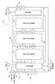
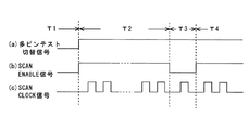
LSIは、外部端子に接続されるバッファと内部回路と間に複数のSFFからなるスキャンチェーンを有し、テストモード時には、このスキャンチェーンを利用してLSIの内部回路にテスト信号を入力する。この場合、外部端子のうち双方向端子111iの出力バッファ3に、多ピンテスト切替信号S101を入力し、これにより双方向端子111iを出力モードに設定すると共に、入力端子112jに出力バッファ14を設け、同じく多ピンテスト切替信号S101により入力端子112jを出力モードに設定する。
【選択図】 図2
Description
1.入力端子及び入力モード時の双方向端子は、端子がオープンになるため、ノイズ等により入力バッファが破壊される
2.テスタに繋がない浮き端子から信号の出し入れができないため、LSI全体の十分なテストを行うことができない
Claims (9)
- 複数の外部端子と、
前記複数の外部端子に接続される内部回路と、
前記複数の外部端子のうちテストモード時に未使用となる未使用外部端子の処理をする未使用端子処理手段と
を有することを特徴とする半導体集積回路装置。 - 前記未使用外部端子と前記内部回路との間に設けられ、該未使用外部端子のそれぞれに接続されるスキャン・フリップフロップからなるシフトレジスタを有する
ことを特徴とする請求項1記載の半導体集積回路装置。 - 前記未使用端子処理手段は、前記未使用外部端子のうち入力端子に接続される出力バッファと、当該出力バッファを出力モードに設定可能な未使用端子制御信号を入力する未使用端子制御信号線とを有し、前記テストモード時に未使用端子制御信号により当該入力端子を出力モードに設定する
ことを特徴とする請求項1又は2に記載の半導体集積回路装置。 - 前記未使用端子制御信号線は、前記未使用端子処理手段の出力バッファに共通に接続されたものであって、
前記未使用端子制御信号線に接続され前記未使用端子制御信号を入力する切替信号入力端子を有する
ことを特徴とする請求項3記載の半導体集積回路装置。 - 前記未使用端子処理手段は、前記未使用外部端子のうち双方向端子に接続される出力バッファを出力モードに設定可能な未使用端子制御信号を入力する未使用端子制御信号線を有し、前記テストモード時に未使用端子制御信号により当該双方向端子を出力モードに設定する
ことを特徴とする請求項1記載の半導体集積回路装置。 - 前記未使用端子処理手段は、前記未使用外部端子のうち双方向端子に接続される出力バッファを通常モード時に出力モードに設定可能な制御信号及び当該出力バッファをテストモード時に出力モードに設定可能な未使用端子制御信号を入力とする論理回路を有し、前記テストモード時に未使用端子制御信号により当該双方向端子を出力モードに設定する
ことを特徴とする請求項1記載の半導体集積回路装置。 - 前記未使用端子処理手段は、前記未使用外部端子のうち入力端子及び/又は双方向端子の電位を固定させる電位固定手段である
を有することを特徴とする請求項1又は2に記載の半導体集積回路装置。 - 前記電位固定手段は、前記未使用外部端子に接続される抵抗と、テストモード時に未使用端子制御信号が入力されて前記抵抗を電源電位又はグランド電位に接続するスイッチとを有する
ことを特徴とする請求項7記載の半導体集積回路装置。 - 前記未使用端子制御信号線は、前記電位固定手段のスイッチに共通に接続されたものであって、
前記未使用端子制御信号線に接続され前記未使用端子制御信号を入力する切替信号入力端子を有する
ことを特徴とする請求項8記載の半導体集積回路装置。
Priority Applications (3)
| Application Number | Priority Date | Filing Date | Title |
|---|---|---|---|
| JP2004094490A JP4610919B2 (ja) | 2004-03-29 | 2004-03-29 | 半導体集積回路装置 |
| EP05004264A EP1584935A1 (en) | 2004-03-29 | 2005-02-26 | Configuration of unused external pins during the test mode in a semiconductor integrated circuit |
| US11/085,149 US7284171B2 (en) | 2004-03-29 | 2005-03-22 | Integrated circuit device |
Applications Claiming Priority (1)
| Application Number | Priority Date | Filing Date | Title |
|---|---|---|---|
| JP2004094490A JP4610919B2 (ja) | 2004-03-29 | 2004-03-29 | 半導体集積回路装置 |
Publications (2)
| Publication Number | Publication Date |
|---|---|
| JP2005283207A true JP2005283207A (ja) | 2005-10-13 |
| JP4610919B2 JP4610919B2 (ja) | 2011-01-12 |
Family
ID=34909424
Family Applications (1)
| Application Number | Title | Priority Date | Filing Date |
|---|---|---|---|
| JP2004094490A Expired - Fee Related JP4610919B2 (ja) | 2004-03-29 | 2004-03-29 | 半導体集積回路装置 |
Country Status (3)
| Country | Link |
|---|---|
| US (1) | US7284171B2 (ja) |
| EP (1) | EP1584935A1 (ja) |
| JP (1) | JP4610919B2 (ja) |
Cited By (2)
| Publication number | Priority date | Publication date | Assignee | Title |
|---|---|---|---|---|
| JP2009164425A (ja) * | 2008-01-08 | 2009-07-23 | Oki Semiconductor Co Ltd | リアルタイムモニタ装置及び動作方法 |
| JP2017201256A (ja) * | 2016-05-06 | 2017-11-09 | 日置電機株式会社 | 測定装置および測定方法 |
Families Citing this family (2)
| Publication number | Priority date | Publication date | Assignee | Title |
|---|---|---|---|---|
| ITVA20050007A1 (it) * | 2005-02-08 | 2006-08-09 | St Microelectronics Srl | Circuito di distribuzione di un segnale di prova applicato su un pad di un dispositivo elettronico |
| EP3435100B1 (en) * | 2017-07-24 | 2020-04-01 | TDK-Micronas GmbH | Method for testing an electronic device and an interface circuit therefore |
Citations (4)
| Publication number | Priority date | Publication date | Assignee | Title |
|---|---|---|---|---|
| JPH0587889A (ja) * | 1991-09-30 | 1993-04-06 | Fujitsu Ltd | 半導体回路素子とその試験処理方法 |
| JPH08105944A (ja) * | 1994-10-06 | 1996-04-23 | Fujitsu Ltd | Mcmに搭載されたlsiの試験方法および装置 |
| JP2001066350A (ja) * | 1999-08-27 | 2001-03-16 | Fuji Electric Co Ltd | 集積回路のテスト方法 |
| JP2001320021A (ja) * | 2000-05-09 | 2001-11-16 | Yaskawa Electric Corp | Asicテスト回路 |
Family Cites Families (9)
| Publication number | Priority date | Publication date | Assignee | Title |
|---|---|---|---|---|
| JPH04213849A (ja) * | 1990-12-10 | 1992-08-04 | Fujitsu Ltd | 半導体装置及びその初期不良検出方法 |
| US5337254A (en) * | 1991-12-16 | 1994-08-09 | Hewlett-Packard Company | Programmable integrated circuit output pad |
| US5459733A (en) * | 1992-03-20 | 1995-10-17 | National Semiconductor Corporation | Input/output checker for a memory array |
| JP3331712B2 (ja) * | 1993-12-21 | 2002-10-07 | セイコーエプソン株式会社 | 半導体装置 |
| US6363505B1 (en) * | 1997-11-14 | 2002-03-26 | Altera Corporation | Programmable control circuit for grounding unused outputs |
| US6016563A (en) * | 1997-12-30 | 2000-01-18 | Fleisher; Evgeny G. | Method and apparatus for testing a logic design of a programmable logic device |
| JP3324583B2 (ja) * | 1999-01-08 | 2002-09-17 | セイコーエプソン株式会社 | 半導体装置及びその製造方法 |
| JP3708493B2 (ja) * | 2001-05-18 | 2005-10-19 | 株式会社ソニー・コンピュータエンタテインメント | デバッグシステム、半導体集積回路、半導体集積回路のデバッグ方法、半導体集積回路のデバッグプログラム、及び半導体集積回路のデバッグプログラムを記録したコンピュータ読み取り可能な記録媒体 |
| JP2003057309A (ja) | 2001-08-16 | 2003-02-26 | Mitsubishi Electric Corp | 半導体集積回路装置 |
-
2004
- 2004-03-29 JP JP2004094490A patent/JP4610919B2/ja not_active Expired - Fee Related
-
2005
- 2005-02-26 EP EP05004264A patent/EP1584935A1/en not_active Withdrawn
- 2005-03-22 US US11/085,149 patent/US7284171B2/en not_active Expired - Lifetime
Patent Citations (4)
| Publication number | Priority date | Publication date | Assignee | Title |
|---|---|---|---|---|
| JPH0587889A (ja) * | 1991-09-30 | 1993-04-06 | Fujitsu Ltd | 半導体回路素子とその試験処理方法 |
| JPH08105944A (ja) * | 1994-10-06 | 1996-04-23 | Fujitsu Ltd | Mcmに搭載されたlsiの試験方法および装置 |
| JP2001066350A (ja) * | 1999-08-27 | 2001-03-16 | Fuji Electric Co Ltd | 集積回路のテスト方法 |
| JP2001320021A (ja) * | 2000-05-09 | 2001-11-16 | Yaskawa Electric Corp | Asicテスト回路 |
Cited By (2)
| Publication number | Priority date | Publication date | Assignee | Title |
|---|---|---|---|---|
| JP2009164425A (ja) * | 2008-01-08 | 2009-07-23 | Oki Semiconductor Co Ltd | リアルタイムモニタ装置及び動作方法 |
| JP2017201256A (ja) * | 2016-05-06 | 2017-11-09 | 日置電機株式会社 | 測定装置および測定方法 |
Also Published As
| Publication number | Publication date |
|---|---|
| JP4610919B2 (ja) | 2011-01-12 |
| US20050216803A1 (en) | 2005-09-29 |
| US7284171B2 (en) | 2007-10-16 |
| EP1584935A1 (en) | 2005-10-12 |
Similar Documents
| Publication | Publication Date | Title |
|---|---|---|
| US6861866B2 (en) | System on chip (SOC) and method of testing and/or debugging the system on chip | |
| JP2009515160A (ja) | 集積回路検査方法及び装置 | |
| JP2007178421A (ja) | 2相クロック制御によるタイミング競合バウンダリスキャンレジスタを用いないシフトレジスタ | |
| JPH11231027A (ja) | 大規模集積回路およびそのボードテスト方法 | |
| US20110175638A1 (en) | Semiconductor integrated circuit and core test circuit | |
| JP2007525684A (ja) | 階層コアのためのテスト回路及び方法 | |
| JP2004110265A (ja) | 半導体集積回路のテスト容易化方法 | |
| US6806731B2 (en) | Semiconductor integrated circuit device and fault-detecting method of a semiconductor integrated circuit device | |
| JP4265934B2 (ja) | スキャンパス回路およびそれを備える論理回路ならびに集積回路のテスト方法 | |
| JP4610919B2 (ja) | 半導体集積回路装置 | |
| US7240263B2 (en) | Apparatus for performing stuck fault testings within an integrated circuit | |
| US20050204227A1 (en) | Semiconductor circuit apparatus and scan test method for semiconductor circuit | |
| JP2024138860A (ja) | 半導体集積回路及び半導体集積回路のテスト方法 | |
| JP5231065B2 (ja) | スキャン用フリップフロップ回路 | |
| JP2004004047A (ja) | 集積回路のための入力/出力特徴付けチェーン | |
| JP2006292646A (ja) | Lsiのテスト方法 | |
| JP4416469B2 (ja) | 半導体集積回路およびその設計方法 | |
| US20040030976A1 (en) | Partial BIST with recording of the connections between individual blocks | |
| KR100532747B1 (ko) | 반도체 집적회로 및 그 설계방법과 반도체 집적회로의 설계프로그램을 기록한 기록매체 | |
| JPH112664A (ja) | バウンダリスキャンレジスタ | |
| JP2010025703A (ja) | 半導体装置およびそのテスト方法 | |
| JP2007003338A (ja) | 半導体装置及びそのテスト方法 | |
| JP2009175154A (ja) | 半導体集積回路およびその設計方法 | |
| JP2874248B2 (ja) | 診断用スキャンパス付き電子回路 | |
| US20050289421A1 (en) | Semiconductor chip |
Legal Events
| Date | Code | Title | Description |
|---|---|---|---|
| A621 | Written request for application examination |
Free format text: JAPANESE INTERMEDIATE CODE: A621 Effective date: 20070110 |
|
| A131 | Notification of reasons for refusal |
Free format text: JAPANESE INTERMEDIATE CODE: A131 Effective date: 20100302 |
|
| A521 | Request for written amendment filed |
Free format text: JAPANESE INTERMEDIATE CODE: A523 Effective date: 20100331 |
|
| TRDD | Decision of grant or rejection written | ||
| A01 | Written decision to grant a patent or to grant a registration (utility model) |
Free format text: JAPANESE INTERMEDIATE CODE: A01 Effective date: 20101012 |
|
| A01 | Written decision to grant a patent or to grant a registration (utility model) |
Free format text: JAPANESE INTERMEDIATE CODE: A01 |
|
| A61 | First payment of annual fees (during grant procedure) |
Free format text: JAPANESE INTERMEDIATE CODE: A61 Effective date: 20101013 |
|
| FPAY | Renewal fee payment (event date is renewal date of database) |
Free format text: PAYMENT UNTIL: 20131022 Year of fee payment: 3 |
|
| R150 | Certificate of patent or registration of utility model |
Free format text: JAPANESE INTERMEDIATE CODE: R150 |
|
| LAPS | Cancellation because of no payment of annual fees |