JP2005285109A - 半導体装置、icカード - Google Patents
半導体装置、icカード Download PDFInfo
- Publication number
- JP2005285109A JP2005285109A JP2005059938A JP2005059938A JP2005285109A JP 2005285109 A JP2005285109 A JP 2005285109A JP 2005059938 A JP2005059938 A JP 2005059938A JP 2005059938 A JP2005059938 A JP 2005059938A JP 2005285109 A JP2005285109 A JP 2005285109A
- Authority
- JP
- Japan
- Prior art keywords
- integrated circuit
- emitting element
- antenna
- light
- light emitting
- Prior art date
- Legal status (The legal status is an assumption and is not a legal conclusion. Google has not performed a legal analysis and makes no representation as to the accuracy of the status listed.)
- Withdrawn
Links
Images










Classifications
-
- H—ELECTRICITY
- H10—SEMICONDUCTOR DEVICES; ELECTRIC SOLID-STATE DEVICES NOT OTHERWISE PROVIDED FOR
- H10D—INORGANIC ELECTRIC SEMICONDUCTOR DEVICES
- H10D86/00—Integrated devices formed in or on insulating or conducting substrates, e.g. formed in silicon-on-insulator [SOI] substrates or on stainless steel or glass substrates
- H10D86/01—Manufacture or treatment
- H10D86/021—Manufacture or treatment of multiple TFTs
- H10D86/0214—Manufacture or treatment of multiple TFTs using temporary substrates
-
- G—PHYSICS
- G06—COMPUTING OR CALCULATING; COUNTING
- G06K—GRAPHICAL DATA READING; PRESENTATION OF DATA; RECORD CARRIERS; HANDLING RECORD CARRIERS
- G06K19/00—Record carriers for use with machines and with at least a part designed to carry digital markings
- G06K19/06—Record carriers for use with machines and with at least a part designed to carry digital markings characterised by the kind of the digital marking, e.g. shape, nature, code
- G06K19/067—Record carriers with conductive marks, printed circuits or semiconductor circuit elements, e.g. credit or identity cards also with resonating or responding marks without active components
- G06K19/07—Record carriers with conductive marks, printed circuits or semiconductor circuit elements, e.g. credit or identity cards also with resonating or responding marks without active components with integrated circuit chips
- G06K19/077—Constructional details, e.g. mounting of circuits in the carrier
-
- G—PHYSICS
- G06—COMPUTING OR CALCULATING; COUNTING
- G06K—GRAPHICAL DATA READING; PRESENTATION OF DATA; RECORD CARRIERS; HANDLING RECORD CARRIERS
- G06K19/00—Record carriers for use with machines and with at least a part designed to carry digital markings
- G06K19/06—Record carriers for use with machines and with at least a part designed to carry digital markings characterised by the kind of the digital marking, e.g. shape, nature, code
- G06K19/067—Record carriers with conductive marks, printed circuits or semiconductor circuit elements, e.g. credit or identity cards also with resonating or responding marks without active components
- G06K19/07—Record carriers with conductive marks, printed circuits or semiconductor circuit elements, e.g. credit or identity cards also with resonating or responding marks without active components with integrated circuit chips
-
- G—PHYSICS
- G06—COMPUTING OR CALCULATING; COUNTING
- G06K—GRAPHICAL DATA READING; PRESENTATION OF DATA; RECORD CARRIERS; HANDLING RECORD CARRIERS
- G06K19/00—Record carriers for use with machines and with at least a part designed to carry digital markings
- G06K19/06—Record carriers for use with machines and with at least a part designed to carry digital markings characterised by the kind of the digital marking, e.g. shape, nature, code
- G06K19/067—Record carriers with conductive marks, printed circuits or semiconductor circuit elements, e.g. credit or identity cards also with resonating or responding marks without active components
- G06K19/07—Record carriers with conductive marks, printed circuits or semiconductor circuit elements, e.g. credit or identity cards also with resonating or responding marks without active components with integrated circuit chips
- G06K19/0723—Record carriers with conductive marks, printed circuits or semiconductor circuit elements, e.g. credit or identity cards also with resonating or responding marks without active components with integrated circuit chips the record carrier comprising an arrangement for non-contact communication, e.g. wireless communication circuits on transponder cards, non-contact smart cards or RFIDs
-
- G—PHYSICS
- G06—COMPUTING OR CALCULATING; COUNTING
- G06K—GRAPHICAL DATA READING; PRESENTATION OF DATA; RECORD CARRIERS; HANDLING RECORD CARRIERS
- G06K19/00—Record carriers for use with machines and with at least a part designed to carry digital markings
- G06K19/06—Record carriers for use with machines and with at least a part designed to carry digital markings characterised by the kind of the digital marking, e.g. shape, nature, code
- G06K19/067—Record carriers with conductive marks, printed circuits or semiconductor circuit elements, e.g. credit or identity cards also with resonating or responding marks without active components
- G06K19/07—Record carriers with conductive marks, printed circuits or semiconductor circuit elements, e.g. credit or identity cards also with resonating or responding marks without active components with integrated circuit chips
- G06K19/0723—Record carriers with conductive marks, printed circuits or semiconductor circuit elements, e.g. credit or identity cards also with resonating or responding marks without active components with integrated circuit chips the record carrier comprising an arrangement for non-contact communication, e.g. wireless communication circuits on transponder cards, non-contact smart cards or RFIDs
- G06K19/0728—Record carriers with conductive marks, printed circuits or semiconductor circuit elements, e.g. credit or identity cards also with resonating or responding marks without active components with integrated circuit chips the record carrier comprising an arrangement for non-contact communication, e.g. wireless communication circuits on transponder cards, non-contact smart cards or RFIDs the arrangement being an optical or sound-based communication interface
-
- G—PHYSICS
- G06—COMPUTING OR CALCULATING; COUNTING
- G06K—GRAPHICAL DATA READING; PRESENTATION OF DATA; RECORD CARRIERS; HANDLING RECORD CARRIERS
- G06K19/00—Record carriers for use with machines and with at least a part designed to carry digital markings
- G06K19/06—Record carriers for use with machines and with at least a part designed to carry digital markings characterised by the kind of the digital marking, e.g. shape, nature, code
- G06K19/067—Record carriers with conductive marks, printed circuits or semiconductor circuit elements, e.g. credit or identity cards also with resonating or responding marks without active components
- G06K19/07—Record carriers with conductive marks, printed circuits or semiconductor circuit elements, e.g. credit or identity cards also with resonating or responding marks without active components with integrated circuit chips
- G06K19/077—Constructional details, e.g. mounting of circuits in the carrier
- G06K19/07749—Constructional details, e.g. mounting of circuits in the carrier the record carrier being capable of non-contact communication, e.g. constructional details of the antenna of a non-contact smart card
-
- G—PHYSICS
- G06—COMPUTING OR CALCULATING; COUNTING
- G06K—GRAPHICAL DATA READING; PRESENTATION OF DATA; RECORD CARRIERS; HANDLING RECORD CARRIERS
- G06K19/00—Record carriers for use with machines and with at least a part designed to carry digital markings
- G06K19/06—Record carriers for use with machines and with at least a part designed to carry digital markings characterised by the kind of the digital marking, e.g. shape, nature, code
- G06K19/08—Record carriers for use with machines and with at least a part designed to carry digital markings characterised by the kind of the digital marking, e.g. shape, nature, code using markings of different kinds or more than one marking of the same kind in the same record carrier, e.g. one marking being sensed by optical and the other by magnetic means
- G06K19/10—Record carriers for use with machines and with at least a part designed to carry digital markings characterised by the kind of the digital marking, e.g. shape, nature, code using markings of different kinds or more than one marking of the same kind in the same record carrier, e.g. one marking being sensed by optical and the other by magnetic means at least one kind of marking being used for authentication, e.g. of credit or identity cards
- G06K19/14—Record carriers for use with machines and with at least a part designed to carry digital markings characterised by the kind of the digital marking, e.g. shape, nature, code using markings of different kinds or more than one marking of the same kind in the same record carrier, e.g. one marking being sensed by optical and the other by magnetic means at least one kind of marking being used for authentication, e.g. of credit or identity cards the marking being sensed by radiation
- G06K19/145—Record carriers for use with machines and with at least a part designed to carry digital markings characterised by the kind of the digital marking, e.g. shape, nature, code using markings of different kinds or more than one marking of the same kind in the same record carrier, e.g. one marking being sensed by optical and the other by magnetic means at least one kind of marking being used for authentication, e.g. of credit or identity cards the marking being sensed by radiation at least one of the further markings being adapted for galvanic or wireless sensing, e.g. an RFID tag with both a wireless and an optical interface or memory, or a contact type smart card with ISO 7816 contacts and an optical interface or memory
-
- H—ELECTRICITY
- H10—SEMICONDUCTOR DEVICES; ELECTRIC SOLID-STATE DEVICES NOT OTHERWISE PROVIDED FOR
- H10D—INORGANIC ELECTRIC SEMICONDUCTOR DEVICES
- H10D86/00—Integrated devices formed in or on insulating or conducting substrates, e.g. formed in silicon-on-insulator [SOI] substrates or on stainless steel or glass substrates
- H10D86/40—Integrated devices formed in or on insulating or conducting substrates, e.g. formed in silicon-on-insulator [SOI] substrates or on stainless steel or glass substrates characterised by multiple TFTs
-
- H—ELECTRICITY
- H10—SEMICONDUCTOR DEVICES; ELECTRIC SOLID-STATE DEVICES NOT OTHERWISE PROVIDED FOR
- H10D—INORGANIC ELECTRIC SEMICONDUCTOR DEVICES
- H10D86/00—Integrated devices formed in or on insulating or conducting substrates, e.g. formed in silicon-on-insulator [SOI] substrates or on stainless steel or glass substrates
- H10D86/40—Integrated devices formed in or on insulating or conducting substrates, e.g. formed in silicon-on-insulator [SOI] substrates or on stainless steel or glass substrates characterised by multiple TFTs
- H10D86/60—Integrated devices formed in or on insulating or conducting substrates, e.g. formed in silicon-on-insulator [SOI] substrates or on stainless steel or glass substrates characterised by multiple TFTs wherein the TFTs are in active matrices
-
- H—ELECTRICITY
- H10—SEMICONDUCTOR DEVICES; ELECTRIC SOLID-STATE DEVICES NOT OTHERWISE PROVIDED FOR
- H10D—INORGANIC ELECTRIC SEMICONDUCTOR DEVICES
- H10D86/00—Integrated devices formed in or on insulating or conducting substrates, e.g. formed in silicon-on-insulator [SOI] substrates or on stainless steel or glass substrates
- H10D86/80—Integrated devices formed in or on insulating or conducting substrates, e.g. formed in silicon-on-insulator [SOI] substrates or on stainless steel or glass substrates characterised by multiple passive components, e.g. resistors, capacitors or inductors
-
- H—ELECTRICITY
- H10—SEMICONDUCTOR DEVICES; ELECTRIC SOLID-STATE DEVICES NOT OTHERWISE PROVIDED FOR
- H10F—INORGANIC SEMICONDUCTOR DEVICES SENSITIVE TO INFRARED RADIATION, LIGHT, ELECTROMAGNETIC RADIATION OF SHORTER WAVELENGTH OR CORPUSCULAR RADIATION
- H10F55/00—Radiation-sensitive semiconductor devices covered by groups H10F10/00, H10F19/00 or H10F30/00 being structurally associated with electric light sources and electrically or optically coupled thereto
- H10F55/10—Radiation-sensitive semiconductor devices covered by groups H10F10/00, H10F19/00 or H10F30/00 being structurally associated with electric light sources and electrically or optically coupled thereto wherein the radiation-sensitive semiconductor devices control the electric light source, e.g. image converters, image amplifiers or image storage devices
- H10F55/15—Radiation-sensitive semiconductor devices covered by groups H10F10/00, H10F19/00 or H10F30/00 being structurally associated with electric light sources and electrically or optically coupled thereto wherein the radiation-sensitive semiconductor devices control the electric light source, e.g. image converters, image amplifiers or image storage devices wherein the radiation-sensitive devices and the electric light source are all semiconductor devices
-
- H—ELECTRICITY
- H10—SEMICONDUCTOR DEVICES; ELECTRIC SOLID-STATE DEVICES NOT OTHERWISE PROVIDED FOR
- H10F—INORGANIC SEMICONDUCTOR DEVICES SENSITIVE TO INFRARED RADIATION, LIGHT, ELECTROMAGNETIC RADIATION OF SHORTER WAVELENGTH OR CORPUSCULAR RADIATION
- H10F99/00—Subject matter not provided for in other groups of this subclass
-
- Y—GENERAL TAGGING OF NEW TECHNOLOGICAL DEVELOPMENTS; GENERAL TAGGING OF CROSS-SECTIONAL TECHNOLOGIES SPANNING OVER SEVERAL SECTIONS OF THE IPC; TECHNICAL SUBJECTS COVERED BY FORMER USPC CROSS-REFERENCE ART COLLECTIONS [XRACs] AND DIGESTS
- Y10—TECHNICAL SUBJECTS COVERED BY FORMER USPC
- Y10S—TECHNICAL SUBJECTS COVERED BY FORMER USPC CROSS-REFERENCE ART COLLECTIONS [XRACs] AND DIGESTS
- Y10S257/00—Active solid-state devices, e.g. transistors, solid-state diodes
- Y10S257/923—Active solid-state devices, e.g. transistors, solid-state diodes with means to optimize electrical conductor current carrying capacity, e.g. particular conductor aspect ratio
Landscapes
- Engineering & Computer Science (AREA)
- Physics & Mathematics (AREA)
- General Physics & Mathematics (AREA)
- Theoretical Computer Science (AREA)
- Computer Hardware Design (AREA)
- Microelectronics & Electronic Packaging (AREA)
- Computer Networks & Wireless Communication (AREA)
- Thin Film Transistor (AREA)
Abstract
【解決手段】 本発明の半導体装置、IDチップ、ICカードは、絶縁分離された薄膜の半導体膜で形成されたTFT(薄膜トランジスタ)が用いられた集積回路を有する。さらに本発明の半導体装置、IDチップ、ICカードは、光電変換を行なうための層に非単結晶の薄膜を用いた、発光素子及び受光素子を有する。発光素子または受光素子は、集積回路と連続して形成(一体形成)されていても良いし、別途形成して集積回路に貼り合わされていても良い。
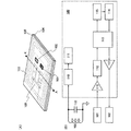
【選択図】 図1
Description

Claims (16)
- アンテナと、集積回路と、発光素子と、受光素子とを有し、
前記集積回路は薄膜トランジスタを有し、
前記発光素子及び前記受光素子は、それぞれ非単結晶の薄膜を用いた、光電変換を行なうための層を有し、
前記アンテナ、前記発光素子及び前記受光素子は、前記集積回路に接続されていることを特徴とする半導体装置。 - アンテナと、集積回路と、発光素子と、受光素子とを有し、
前記集積回路は薄膜トランジスタを有し、
前記アンテナ、前記発光素子及び前記受光素子は、前記集積回路に接続されており、
前記集積回路、前記発光素子及び前記受光素子は、一体形成されていることを特徴とする半導体装置。 - アンテナと、集積回路と、発光素子と、受光素子とを有し、
前記集積回路は薄膜トランジスタを有し、
前記アンテナ、前記発光素子及び前記受光素子は、前記集積回路に接続されており、
前記アンテナ、前記集積回路、前記発光素子及び前記受光素子は、一体形成されていることを特徴とする半導体装置。 - 集積回路と、発光素子と、受光素子とを有し、
前記集積回路は、接続端子と、アンテナによって前記接続端子に入力された交流の信号から電源電圧を生成する整流回路と、前記受光素子において受信した第1の信号を復調する復調回路と、復調された前記第1の信号に従って演算処理を行ない第2の信号を生成する論理回路とを有し、
前記発光素子は前記第2の信号を光信号に変換することができ、
前記集積回路、前記発光素子及び前記受光素子は、一体形成されていることを特徴とする半導体装置。 - アンテナと、集積回路と、発光素子と、受光素子とを有し、
前記集積回路は薄膜トランジスタを有し、
前記発光素子及び前記受光素子は、それぞれ非単結晶の薄膜を用いた、光電変換を行なうための層を有し、
前記アンテナ、前記発光素子及び前記受光素子は、前記集積回路に接続されており、
前記集積回路、前記発光素子及び前記受光素子は、第1の基板上に形成された後、剥離され、第2の基板上に貼り合わされていることを特徴とする半導体装置。 - アンテナと、集積回路と、発光素子と、受光素子とを有し、
前記集積回路は薄膜トランジスタを有し、
前記アンテナ、前記発光素子及び前記受光素子は、前記集積回路に接続されており、
前記集積回路、前記発光素子及び前記受光素子は、第1の基板上に形成された後、剥離され、第2の基板上に貼り合わされていることを特徴とする半導体装置。 - アンテナと、集積回路と、発光素子と、受光素子とを有し、
前記集積回路は薄膜トランジスタを有し、
前記アンテナ、前記発光素子及び前記受光素子は、前記集積回路に接続されており、
前記アンテナ、前記集積回路、前記発光素子及び前記受光素子は、第1の基板上に形成された後、剥離され、第2の基板上に貼り合わされていることを特徴とする半導体装置。 - 集積回路と、発光素子と、受光素子とを有し、
前記集積回路は、接続端子と、アンテナによって前記接続端子に入力された交流の信号から電源電圧を生成する整流回路と、前記受光素子において受信した第1の信号を復調する復調回路と、復調された前記第1の信号に従って演算処理を行ない第2の信号を生成する論理回路とを有し、
前記発光素子は前記第2の信号を光信号に変換することができ、
前記集積回路、前記発光素子及び前記受光素子は、一体形成されており、
前記集積回路、前記発光素子及び前記受光素子は、第1の基板上に形成された後、剥離され、第2の基板上に貼り合わされていることを特徴とする半導体装置。 - 請求項5乃至8のいずれか一項において、
前記第1の基板はガラスであり、前記第2の基板はプラスチックであることを特徴とする半導体装置。 - アンテナと、集積回路と、発光素子と、受光素子とを有し、
前記集積回路は薄膜トランジスタを有し、
前記アンテナ、前記発光素子及び前記受光素子は、前記集積回路に接続されており、
前記集積回路、前記発光素子及び前記受光素子は、一体形成されていることを特徴とするICカード。 - アンテナと、集積回路と、発光素子と、受光素子とを有し、
前記集積回路は薄膜トランジスタを有し、
前記アンテナ、前記発光素子及び前記受光素子は、前記集積回路に接続されており、
前記アンテナ、前記集積回路、前記発光素子及び前記受光素子は、一体形成されていることを特徴とするICカード。 - 集積回路と、発光素子と、受光素子とを有し、
前記集積回路は、接続端子と、アンテナによって前記接続端子に入力された交流の信号から電源電圧を生成する整流回路と、前記受光素子において受信した第1の信号を復調する復調回路と、復調された前記第1の信号に従って演算処理を行ない第2の信号を生成する論理回路とを有し、
前記発光素子は前記第2の信号を光信号に変換することができ、
前記集積回路、前記発光素子及び前記受光素子は、一体形成されていることを特徴とするICカード。 - アンテナと、集積回路と、発光素子と、受光素子とを有し、
前記集積回路は薄膜トランジスタを有し、
前記アンテナ、前記発光素子及び前記受光素子は、前記集積回路に接続されており、
前記集積回路、前記発光素子及び前記受光素子は、第1の基板上に形成された後、剥離され、第2の基板上に貼り合わされていることを特徴とするICカード。 - アンテナと、集積回路と、発光素子と、受光素子とを有し、
前記集積回路は薄膜トランジスタを有し、
前記アンテナ、前記発光素子及び前記受光素子は、前記集積回路に接続されており、
前記アンテナ、前記集積回路、前記発光素子及び前記受光素子は、第1の基板上に形成された後、剥離され、第2の基板上に貼り合わされていることを特徴とするICカード。 - 集積回路と、発光素子と、受光素子とを有し、
前記集積回路は、接続端子と、アンテナによって前記接続端子に入力された交流の信号から電源電圧を生成する整流回路と、前記受光素子において受信した第1の信号を復調する復調回路と、復調された前記第1の信号に従って演算処理を行ない第2の信号を生成する論理回路とを有し、
前記発光素子は前記第2の信号を光信号に変換することができ、
前記集積回路、前記発光素子及び前記受光素子は、一体形成されており、
前記集積回路、前記発光素子及び前記受光素子は、第1の基板上に形成された後、剥離され、第2の基板上に貼り合わされていることを特徴とするICカード。 - 請求項13乃至15のいずれか一項において、
前記第1の基板はガラスであり、前記第2の基板はプラスチックであることを特徴とするICカード。
Priority Applications (1)
| Application Number | Priority Date | Filing Date | Title |
|---|---|---|---|
| JP2005059938A JP2005285109A (ja) | 2004-03-04 | 2005-03-04 | 半導体装置、icカード |
Applications Claiming Priority (2)
| Application Number | Priority Date | Filing Date | Title |
|---|---|---|---|
| JP2004060103 | 2004-03-04 | ||
| JP2005059938A JP2005285109A (ja) | 2004-03-04 | 2005-03-04 | 半導体装置、icカード |
Publications (2)
| Publication Number | Publication Date |
|---|---|
| JP2005285109A true JP2005285109A (ja) | 2005-10-13 |
| JP2005285109A5 JP2005285109A5 (ja) | 2008-04-10 |
Family
ID=34918006
Family Applications (1)
| Application Number | Title | Priority Date | Filing Date |
|---|---|---|---|
| JP2005059938A Withdrawn JP2005285109A (ja) | 2004-03-04 | 2005-03-04 | 半導体装置、icカード |
Country Status (5)
| Country | Link |
|---|---|
| US (3) | US8030745B2 (ja) |
| JP (1) | JP2005285109A (ja) |
| KR (1) | KR101098777B1 (ja) |
| CN (1) | CN100478986C (ja) |
| WO (1) | WO2005086088A1 (ja) |
Cited By (15)
| Publication number | Priority date | Publication date | Assignee | Title |
|---|---|---|---|---|
| JP2007172592A (ja) * | 2005-11-25 | 2007-07-05 | Semiconductor Energy Lab Co Ltd | 半導体装置 |
| WO2007077850A1 (en) * | 2005-12-27 | 2007-07-12 | Semiconductor Energy Laboratory Co., Ltd. | Semiconductor device and manufacturing method thereof |
| WO2008013007A1 (fr) * | 2006-07-27 | 2008-01-31 | Kabushiki Kaisha Toshiba | Procédé de fabrication d'entrée de carte sans fil, procédé de fabrication de carte sans fil, entrée de carte sans fil et carte sans fil |
| WO2008065993A1 (fr) * | 2006-11-28 | 2008-06-05 | Philtech Inc. | Particule de poudre rf, poudre rf et procédé d'excitation de poudre rf |
| KR100968489B1 (ko) | 2008-06-17 | 2010-07-07 | 재단법인서울대학교산학협력재단 | 데이터 저장 입자 및 데이터 전송 시스템 |
| WO2010086904A1 (ja) * | 2009-02-02 | 2010-08-05 | 新田工業株式会社 | Icタグ |
| CN102135577A (zh) * | 2010-12-29 | 2011-07-27 | 中山达华智能科技股份有限公司 | 一种跟踪电子电器产品使用寿命的方法及装置 |
| US8178415B2 (en) | 2006-11-27 | 2012-05-15 | Philtech, Inc. | Method for manufacturing RF powder |
| US8237622B2 (en) | 2006-12-28 | 2012-08-07 | Philtech Inc. | Base sheet |
| US8318047B2 (en) | 2006-11-28 | 2012-11-27 | Philtech, Inc. | Method for providing RF powder and RF powder-containing liquid |
| WO2013039395A1 (en) * | 2011-09-14 | 2013-03-21 | Ec Solution Group B.V. | Active matrix display smart card |
| JP5294042B2 (ja) * | 2009-09-28 | 2013-09-18 | アイシン精機株式会社 | ドア開閉装置 |
| US8766802B2 (en) | 2006-11-27 | 2014-07-01 | Philtech Inc. | Base data management system |
| US8766853B2 (en) | 2006-11-27 | 2014-07-01 | Philtech Inc. | Method for adding RF powder and RF powder-added base sheet |
| US8933784B2 (en) | 2006-11-28 | 2015-01-13 | Philtech Inc. | RF powder particle, RF powder, and RF powder-containing base |
Families Citing this family (45)
| Publication number | Priority date | Publication date | Assignee | Title |
|---|---|---|---|---|
| US8030745B2 (en) * | 2004-03-04 | 2011-10-04 | Semiconductor Energy Laboratory Co., Ltd. | ID chip and IC card |
| US7681232B2 (en) * | 2004-03-08 | 2010-03-16 | Cardlab Aps | Credit card and a secured data activation system |
| WO2006001287A1 (en) * | 2004-06-24 | 2006-01-05 | Semiconductor Energy Laboratory Co., Ltd. | Method for manufacturing thin film integrated circuit |
| WO2006078065A1 (en) | 2005-01-21 | 2006-07-27 | Semiconductor Energy Laboratory Co., Ltd. | Semiconductor device |
| US7605056B2 (en) | 2005-05-31 | 2009-10-20 | Semiconductor Energy Laboratory Co., Ltd. | Method of manufacturing a semiconductor device including separation by physical force |
| US7799654B2 (en) * | 2005-08-31 | 2010-09-21 | Taiwan Semiconductor Manufacturing Company, Ltd. | Reduced refractive index and extinction coefficient layer for enhanced photosensitivity |
| US8232621B2 (en) * | 2006-07-28 | 2012-07-31 | Semiconductor Energy Laboratory Co., Ltd. | Semiconductor device |
| KR101478810B1 (ko) | 2006-07-28 | 2015-01-02 | 가부시키가이샤 한도오따이 에네루기 켄큐쇼 | 축전 장치 |
| JP2008136019A (ja) * | 2006-11-29 | 2008-06-12 | Philtech Inc | 磁界結合装置および読取り装置 |
| US7750852B2 (en) * | 2007-04-13 | 2010-07-06 | Semiconductor Energy Laboratory Co., Ltd. | Semiconductor device |
| JP2009087928A (ja) * | 2007-09-13 | 2009-04-23 | Semiconductor Energy Lab Co Ltd | 半導体装置およびその作製方法 |
| US7764498B2 (en) | 2007-09-24 | 2010-07-27 | Sixis, Inc. | Comb-shaped power bus bar assembly structure having integrated capacitors |
| US20090159709A1 (en) * | 2007-12-24 | 2009-06-25 | Dynamics Inc. | Advanced dynamic credit cards |
| WO2011022099A2 (en) * | 2009-05-29 | 2011-02-24 | Arizona Board Of Regents, For And On Behalf Of Arizona State University | Flexible identification systems and related methods |
| TWI424574B (zh) * | 2009-07-28 | 2014-01-21 | Prime View Int Co Ltd | 數位x光探測面板及其製作方法 |
| DE102010019615A1 (de) * | 2010-05-06 | 2011-11-10 | Rat Asset & Trading Ag | Karte zur elektronischen Zugangskontrolle |
| KR101235942B1 (ko) * | 2010-08-13 | 2013-02-21 | 임은석 | 인레이 시트 및 그 제조 방법 |
| JP2012043689A (ja) * | 2010-08-20 | 2012-03-01 | Toshiba Tec Corp | 有機el装置の製造方法 |
| US9781783B2 (en) * | 2011-04-15 | 2017-10-03 | Semiconductor Energy Laboratory Co., Ltd. | Light-emitting device, display device, light-emitting system, and display system |
| US8649820B2 (en) | 2011-11-07 | 2014-02-11 | Blackberry Limited | Universal integrated circuit card apparatus and related methods |
| US8763914B2 (en) * | 2012-01-17 | 2014-07-01 | On Track Innovations Ltd. | Decoupled contactless bi-directional systems and methods |
| US8936199B2 (en) | 2012-04-13 | 2015-01-20 | Blackberry Limited | UICC apparatus and related methods |
| USD703208S1 (en) * | 2012-04-13 | 2014-04-22 | Blackberry Limited | UICC apparatus |
| USD701864S1 (en) * | 2012-04-23 | 2014-04-01 | Blackberry Limited | UICC apparatus |
| US9269032B2 (en) * | 2012-10-28 | 2016-02-23 | Zlotech Llc | Glass-containing transaction card and method of making the same |
| USD707682S1 (en) * | 2012-12-05 | 2014-06-24 | Logomotion, S.R.O. | Memory card |
| USD759022S1 (en) * | 2013-03-13 | 2016-06-14 | Nagrastar Llc | Smart card interface |
| US9647997B2 (en) | 2013-03-13 | 2017-05-09 | Nagrastar, Llc | USB interface for performing transport I/O |
| USD729808S1 (en) | 2013-03-13 | 2015-05-19 | Nagrastar Llc | Smart card interface |
| USD758372S1 (en) * | 2013-03-13 | 2016-06-07 | Nagrastar Llc | Smart card interface |
| US9888283B2 (en) | 2013-03-13 | 2018-02-06 | Nagrastar Llc | Systems and methods for performing transport I/O |
| SG11201509289UA (en) | 2013-04-12 | 2015-12-30 | Cardlab Aps | A card, an assembly, a method of assembling the card and a method of outputting information |
| KR20160005709A (ko) | 2013-04-12 | 2016-01-15 | 카드랩 에이피에스 | 오프셋 필드 생성기를 갖는 카드 |
| DE102014018393A1 (de) * | 2014-10-14 | 2016-04-14 | Infineon Technologies Ag | Chipkartenmodul-Anordnung, Chipkarten-Anordnung und Verfahren zum Herstellen einer Chipkarten-Anordnung |
| CN104485334B (zh) * | 2014-12-16 | 2018-02-13 | 京东方科技集团股份有限公司 | 阵列基板及其制作方法、显示装置 |
| EP3035230A1 (en) | 2014-12-19 | 2016-06-22 | Cardlab ApS | A method and an assembly for generating a magnetic field |
| MA41187A (fr) | 2014-12-19 | 2021-04-07 | Cardlab Aps | Procédé et ensemble pour générer un champ magnétique et procédé de fabrication d'un ensemble |
| US9436941B1 (en) * | 2015-02-18 | 2016-09-06 | Calay Venture S.à.r.l. | Smart payment instruments |
| USD780763S1 (en) | 2015-03-20 | 2017-03-07 | Nagrastar Llc | Smart card interface |
| EP3082071A1 (en) | 2015-04-17 | 2016-10-19 | Cardlab ApS | Device for and method of outputting a magnetic field |
| USD864968S1 (en) | 2015-04-30 | 2019-10-29 | Echostar Technologies L.L.C. | Smart card interface |
| USD776664S1 (en) * | 2015-05-20 | 2017-01-17 | Chaya Coleena Hendrick | Smart card |
| TWI655394B (zh) * | 2017-09-29 | 2019-04-01 | 凱祿光電股份有限公司 | 發光裝置及其驅動方法 |
| CN109993243A (zh) * | 2019-03-05 | 2019-07-09 | 浙江大学 | 一种基于透明薄膜rfid芯片的商品防伪追溯系统 |
| CN215814237U (zh) * | 2021-08-26 | 2022-02-11 | 捷德(中国)科技有限公司 | 智能卡 |
Citations (6)
| Publication number | Priority date | Publication date | Assignee | Title |
|---|---|---|---|---|
| JPH0425497A (ja) * | 1990-05-21 | 1992-01-29 | Casio Comput Co Ltd | Icカード |
| JPH1120360A (ja) * | 1997-07-03 | 1999-01-26 | Seiko Epson Corp | Icカード及び薄膜集積回路装置並びにそれらの製造方法 |
| JP2001155134A (ja) * | 1999-11-30 | 2001-06-08 | Seiko Epson Corp | 半導体回路内蔵構造体 |
| JP2001257292A (ja) * | 2000-03-10 | 2001-09-21 | Hitachi Maxell Ltd | 半導体装置 |
| JP2002083894A (ja) * | 2000-06-21 | 2002-03-22 | Hitachi Maxell Ltd | 半導体チップ及びこれを用いた半導体装置 |
| JP2002231909A (ja) * | 2001-01-31 | 2002-08-16 | Canon Inc | 薄膜半導体装置の製造方法 |
Family Cites Families (19)
| Publication number | Priority date | Publication date | Assignee | Title |
|---|---|---|---|---|
| US4575621A (en) * | 1984-03-07 | 1986-03-11 | Corpra Research, Inc. | Portable electronic transaction device and system therefor |
| US4695859A (en) * | 1986-10-20 | 1987-09-22 | Energy Conversion Devices, Inc. | Thin film light emitting diode, photonic circuit employing said diode imager employing said circuits |
| AU7238187A (en) * | 1986-12-01 | 1988-06-30 | Ronald W. Froelich | Computerized data-bearing card and reader/writer therefor |
| US4829166A (en) | 1986-12-01 | 1989-05-09 | Froelich Ronald W | Computerized data-bearing card and reader/writer therefor |
| JP3448450B2 (ja) * | 1996-04-26 | 2003-09-22 | 三洋電機株式会社 | 発光素子およびその製造方法 |
| US5789733A (en) * | 1996-09-20 | 1998-08-04 | Motorola, Inc. | Smart card with contactless optical interface |
| JPH10270535A (ja) * | 1997-03-25 | 1998-10-09 | Nikon Corp | 移動ステージ装置、及び該ステージ装置を用いた回路デバイス製造方法 |
| JPH10321883A (ja) | 1997-05-16 | 1998-12-04 | Semiconductor Energy Lab Co Ltd | 太陽電池およびその作製方法 |
| EP0975027A2 (en) * | 1998-07-23 | 2000-01-26 | Sony Corporation | Light emitting device and process for producing the same |
| JP4562844B2 (ja) * | 2000-02-23 | 2010-10-13 | 浜松ホトニクス株式会社 | 光電陰極及び電子管 |
| US20010030511A1 (en) * | 2000-04-18 | 2001-10-18 | Shunpei Yamazaki | Display device |
| US6838773B2 (en) * | 2000-06-21 | 2005-01-04 | Hitachi Maxell, Ltd. | Semiconductor chip and semiconductor device using the semiconductor chip |
| JP4703883B2 (ja) * | 2001-04-09 | 2011-06-15 | 株式会社半導体エネルギー研究所 | 半導体装置の作製方法 |
| JP3886339B2 (ja) * | 2001-04-11 | 2007-02-28 | シャープ株式会社 | 半導体装置 |
| US7218349B2 (en) * | 2001-08-09 | 2007-05-15 | Semiconductor Energy Laboratory Co., Ltd. | Semiconductor device |
| US7204425B2 (en) * | 2002-03-18 | 2007-04-17 | Precision Dynamics Corporation | Enhanced identification appliance |
| JP4366921B2 (ja) * | 2002-07-12 | 2009-11-18 | セイコーエプソン株式会社 | 本人照合装置、カード型情報記録媒体及びそれを用いた情報処理システム |
| JP4401657B2 (ja) * | 2003-01-10 | 2010-01-20 | 株式会社半導体エネルギー研究所 | 発光装置の製造方法 |
| US8030745B2 (en) * | 2004-03-04 | 2011-10-04 | Semiconductor Energy Laboratory Co., Ltd. | ID chip and IC card |
-
2005
- 2005-02-28 US US10/590,271 patent/US8030745B2/en not_active Expired - Fee Related
- 2005-02-28 CN CNB2005800068836A patent/CN100478986C/zh not_active Expired - Fee Related
- 2005-02-28 WO PCT/JP2005/003804 patent/WO2005086088A1/en not_active Ceased
- 2005-02-28 KR KR1020067020851A patent/KR101098777B1/ko not_active Expired - Fee Related
- 2005-03-04 JP JP2005059938A patent/JP2005285109A/ja not_active Withdrawn
-
2011
- 2011-09-21 US US13/238,763 patent/US9449999B2/en not_active Expired - Fee Related
-
2016
- 2016-09-15 US US15/266,408 patent/US20170004393A1/en not_active Abandoned
Patent Citations (6)
| Publication number | Priority date | Publication date | Assignee | Title |
|---|---|---|---|---|
| JPH0425497A (ja) * | 1990-05-21 | 1992-01-29 | Casio Comput Co Ltd | Icカード |
| JPH1120360A (ja) * | 1997-07-03 | 1999-01-26 | Seiko Epson Corp | Icカード及び薄膜集積回路装置並びにそれらの製造方法 |
| JP2001155134A (ja) * | 1999-11-30 | 2001-06-08 | Seiko Epson Corp | 半導体回路内蔵構造体 |
| JP2001257292A (ja) * | 2000-03-10 | 2001-09-21 | Hitachi Maxell Ltd | 半導体装置 |
| JP2002083894A (ja) * | 2000-06-21 | 2002-03-22 | Hitachi Maxell Ltd | 半導体チップ及びこれを用いた半導体装置 |
| JP2002231909A (ja) * | 2001-01-31 | 2002-08-16 | Canon Inc | 薄膜半導体装置の製造方法 |
Cited By (20)
| Publication number | Priority date | Publication date | Assignee | Title |
|---|---|---|---|---|
| JP2007172592A (ja) * | 2005-11-25 | 2007-07-05 | Semiconductor Energy Lab Co Ltd | 半導体装置 |
| KR101233639B1 (ko) | 2005-12-27 | 2013-02-15 | 가부시키가이샤 한도오따이 에네루기 켄큐쇼 | 반도체장치 및 그 제조방법 |
| WO2007077850A1 (en) * | 2005-12-27 | 2007-07-12 | Semiconductor Energy Laboratory Co., Ltd. | Semiconductor device and manufacturing method thereof |
| JP2007200291A (ja) * | 2005-12-27 | 2007-08-09 | Semiconductor Energy Lab Co Ltd | 半導体装置およびその作製方法 |
| US9177242B2 (en) | 2005-12-27 | 2015-11-03 | Semiconductor Energy Laboratory Co., Ltd. | Semiconductor device and manufacturing method thereof |
| US8476632B2 (en) | 2005-12-27 | 2013-07-02 | Semiconductor Energy Laboratory Co., Ltd. | Semiconductor device and manufacturing method thereof |
| WO2008013007A1 (fr) * | 2006-07-27 | 2008-01-31 | Kabushiki Kaisha Toshiba | Procédé de fabrication d'entrée de carte sans fil, procédé de fabrication de carte sans fil, entrée de carte sans fil et carte sans fil |
| US8766853B2 (en) | 2006-11-27 | 2014-07-01 | Philtech Inc. | Method for adding RF powder and RF powder-added base sheet |
| US8766802B2 (en) | 2006-11-27 | 2014-07-01 | Philtech Inc. | Base data management system |
| US8178415B2 (en) | 2006-11-27 | 2012-05-15 | Philtech, Inc. | Method for manufacturing RF powder |
| US8704202B2 (en) | 2006-11-28 | 2014-04-22 | Philtech Inc. | RF powder particles including an inductance element, a capacitance element, and a photovoltaic cell and method for exciting RF powder |
| US8318047B2 (en) | 2006-11-28 | 2012-11-27 | Philtech, Inc. | Method for providing RF powder and RF powder-containing liquid |
| US8933784B2 (en) | 2006-11-28 | 2015-01-13 | Philtech Inc. | RF powder particle, RF powder, and RF powder-containing base |
| WO2008065993A1 (fr) * | 2006-11-28 | 2008-06-05 | Philtech Inc. | Particule de poudre rf, poudre rf et procédé d'excitation de poudre rf |
| US8237622B2 (en) | 2006-12-28 | 2012-08-07 | Philtech Inc. | Base sheet |
| KR100968489B1 (ko) | 2008-06-17 | 2010-07-07 | 재단법인서울대학교산학협력재단 | 데이터 저장 입자 및 데이터 전송 시스템 |
| WO2010086904A1 (ja) * | 2009-02-02 | 2010-08-05 | 新田工業株式会社 | Icタグ |
| JP5294042B2 (ja) * | 2009-09-28 | 2013-09-18 | アイシン精機株式会社 | ドア開閉装置 |
| CN102135577A (zh) * | 2010-12-29 | 2011-07-27 | 中山达华智能科技股份有限公司 | 一种跟踪电子电器产品使用寿命的方法及装置 |
| WO2013039395A1 (en) * | 2011-09-14 | 2013-03-21 | Ec Solution Group B.V. | Active matrix display smart card |
Also Published As
| Publication number | Publication date |
|---|---|
| WO2005086088A1 (en) | 2005-09-15 |
| KR20070007134A (ko) | 2007-01-12 |
| US20070176622A1 (en) | 2007-08-02 |
| US9449999B2 (en) | 2016-09-20 |
| CN1926561A (zh) | 2007-03-07 |
| US20120007096A1 (en) | 2012-01-12 |
| CN100478986C (zh) | 2009-04-15 |
| US20170004393A1 (en) | 2017-01-05 |
| US8030745B2 (en) | 2011-10-04 |
| KR101098777B1 (ko) | 2011-12-28 |
Similar Documents
| Publication | Publication Date | Title |
|---|---|---|
| JP2005285109A (ja) | 半導体装置、icカード | |
| KR101161361B1 (ko) | 반도체장치 | |
| JP5323382B2 (ja) | 半導体装置 | |
| US8546912B2 (en) | Semiconductor device | |
| US9935363B2 (en) | Semiconductor device | |
| CN100521117C (zh) | 半导体器件及其制造方法 | |
| JP4610348B2 (ja) | 半導体装置 | |
| JP2005340791A (ja) | Mos容量素子及び半導体装置 | |
| JP4566794B2 (ja) | 半導体装置 | |
| JP4718863B2 (ja) | 半導体装置及び半導体装置の作製方法 | |
| JP5041672B2 (ja) | 半導体装置 | |
| JP4545617B2 (ja) | 半導体装置 | |
| JP2005252243A (ja) | 半導体装置 |
Legal Events
| Date | Code | Title | Description |
|---|---|---|---|
| A521 | Request for written amendment filed |
Free format text: JAPANESE INTERMEDIATE CODE: A523 Effective date: 20080225 |
|
| A621 | Written request for application examination |
Free format text: JAPANESE INTERMEDIATE CODE: A621 Effective date: 20080225 |
|
| A131 | Notification of reasons for refusal |
Free format text: JAPANESE INTERMEDIATE CODE: A131 Effective date: 20101102 |
|
| A521 | Request for written amendment filed |
Free format text: JAPANESE INTERMEDIATE CODE: A523 Effective date: 20101213 |
|
| A02 | Decision of refusal |
Free format text: JAPANESE INTERMEDIATE CODE: A02 Effective date: 20110322 |
|
| A761 | Written withdrawal of application |
Free format text: JAPANESE INTERMEDIATE CODE: A761 Effective date: 20110405 |