JP2005290171A - Adhesive film for semiconductor and semiconductor device - Google Patents
Adhesive film for semiconductor and semiconductor device Download PDFInfo
- Publication number
- JP2005290171A JP2005290171A JP2004106274A JP2004106274A JP2005290171A JP 2005290171 A JP2005290171 A JP 2005290171A JP 2004106274 A JP2004106274 A JP 2004106274A JP 2004106274 A JP2004106274 A JP 2004106274A JP 2005290171 A JP2005290171 A JP 2005290171A
- Authority
- JP
- Japan
- Prior art keywords
- semiconductor
- adhesive film
- resin
- weight
- thermosetting resin
- Prior art date
- Legal status (The legal status is an assumption and is not a legal conclusion. Google has not performed a legal analysis and makes no representation as to the accuracy of the status listed.)
- Pending
Links
Landscapes
- Manufacture Of Macromolecular Shaped Articles (AREA)
- Compositions Of Macromolecular Compounds (AREA)
- Die Bonding (AREA)
Abstract
Description
本発明は、半導体用接着フィルム及び半導体装置に関する。 The present invention relates to an adhesive film for a semiconductor and a semiconductor device.
近年、電子機器の高機能化等に対応して半導体装置の高密度化、高集積化の要求が強まり、半導体パッケージの大容量高密度化が進んでいる。このような要求に対応するため、例えば半導体素子の上にリードを接着するリード・オン・チップ(LOC)構造が採用されている。LOC構造では、半導体素子とリードフレームとを接合するため、その接合部での接着信頼性が半導体パッケージの信頼性に大きく影響している。 In recent years, there has been an increasing demand for higher density and higher integration of semiconductor devices in response to higher functions of electronic devices, and semiconductor packages have been increasing in capacity and density. In order to meet such requirements, for example, a lead-on-chip (LOC) structure in which a lead is bonded onto a semiconductor element is employed. In the LOC structure, since the semiconductor element and the lead frame are bonded, the reliability of bonding at the bonded portion greatly affects the reliability of the semiconductor package.
従来、半導体素子とリードフレームとの接着には、ペースト状接着剤が用いられている。ペースト状接着剤をリードフレームに薄く均一にかつ適量塗布することは困難であり、半導体素子やリードフレームから接着剤がはみ出すことがあった。 Conventionally, a paste adhesive is used for bonding a semiconductor element and a lead frame. It is difficult to apply an appropriate amount of paste adhesive to the lead frame in a thin and uniform manner, and the adhesive sometimes protrudes from the semiconductor element or the lead frame.
例えばLOC構造ではポリイミド樹脂を用いたホットメルト型の接着剤フィルム等の耐熱性基材に接着剤を塗布したフィルム状接着剤が用いられてきている(例えば、特許文献1参照)。ホットメルト型の接着剤フィルムは、高温で接着する必要があるため、高密度化した半導体素子、リードフレームに熱損傷を与える場合があった。 For example, in the LOC structure, a film adhesive in which an adhesive is applied to a heat resistant substrate such as a hot-melt adhesive film using a polyimide resin has been used (for example, see Patent Document 1). Since the hot melt type adhesive film needs to be bonded at a high temperature, it may cause thermal damage to the densified semiconductor element and lead frame.
特に近年の半導体パッケージはチップの上にチップを多段で積層することでパッケージ
の小型化、薄型化、大容量化を実現している。そういったパッケージにはリードフレームに代わりビスマレイミド−トリアジン基板やポリイミド基板のような有機基板の使用が増加している。こういった有機基板の増加とともにパッケージをはんだ付けするための赤外線リフロー時に密着性不良によるパッケージクラックが技術課題となっており特に半導体素子接着剤の寄与するところが大きいことが分かっている。
本発明の目的は、半導体素子とリードフレーム、有機基板等の半導体素子搭載用支持部材とを接着することができ低温接着性および高温での密着性に優れた半導体用接着フィルムおよび半導体装置を提供することである。 An object of the present invention is to provide a semiconductor adhesive film and a semiconductor device that can adhere a semiconductor element and a support member for mounting a semiconductor element such as a lead frame or an organic substrate and have excellent low-temperature adhesion and high-temperature adhesion. It is to be.
このような目的は、下記(1)〜(6)に記載の本発明により達成される。
(1)アクリル酸共重合体、第一の熱硬化性樹脂及び第二の熱硬化性樹脂を含む樹脂組成物を用いて形成してなることを特徴とする半導体用接着フィルム。
(2) 前記第一の熱硬化性樹脂及び第二の熱硬化性樹脂をエポキシ樹脂とする第(1)項記載の半導体用接着フィルム。
(3) 第一の熱硬化樹脂の融点Aと、第二の熱硬化樹脂の融点Bとが、A>Bとなる第(1)又は(2)項記載の半導体用接着フィルム。
(4)第一の熱硬化性樹脂の融点Aが70〜150℃となる第(1)〜(3)項記載の半導体用接着フィルム。
(5)第二の熱硬化性樹脂の融点Bが30〜80℃となる第(1)〜(4)項記載の半導体用接着フィルム。
(6) 第(1)〜(5)項のいずれか1項に記載の半導体用接着フィルムを用いて、半導体素子と半導体素子搭載用支持部材とを接合していることを特徴とする半導体装置。
Such an object is achieved by the present invention described in the following (1) to (6).
(1) An adhesive film for a semiconductor formed by using a resin composition containing an acrylic acid copolymer, a first thermosetting resin, and a second thermosetting resin.
(2) The adhesive film for a semiconductor according to (1), wherein the first thermosetting resin and the second thermosetting resin are epoxy resins.
(3) The adhesive film for a semiconductor according to (1) or (2), wherein the melting point A of the first thermosetting resin and the melting point B of the second thermosetting resin satisfy A> B.
(4) The adhesive film for a semiconductor according to (1) to (3), wherein the melting point A of the first thermosetting resin is 70 to 150 ° C.
(5) The adhesive film for a semiconductor according to (1) to (4), wherein the melting point B of the second thermosetting resin is 30 to 80 ° C.
(6) A semiconductor device characterized in that a semiconductor element and a semiconductor element mounting support member are joined using the adhesive film for a semiconductor according to any one of (1) to (5). .
本発明によれば、半導体素子とリードフレーム、有機基板等の半導体素子搭載用支持部材とを接着することができ低温接着性および高温での密着性の優れた半導体用接着フィルムおよび半導体装置を提供することができる。 According to the present invention, there are provided a semiconductor adhesive film and a semiconductor device capable of adhering a semiconductor element and a support member for mounting a semiconductor element such as a lead frame and an organic substrate and having excellent low-temperature adhesion and high-temperature adhesion. can do.
本発明の半導体用接着フィルムは、アクリル酸共重合体、第一の熱硬化性樹脂及び第二
の熱硬化性樹脂を含有してなる樹脂組成物からなることを特徴とする。
The adhesive film for semiconductor of the present invention is characterized by comprising a resin composition containing an acrylic acid copolymer, a first thermosetting resin, and a second thermosetting resin.
本発明に用いるアクリル酸共重合体のは、接着力の向上、凝集力の向上という点で優れている。またアクリル酸共重合体のガラス転移温度は−20〜120℃であることが好ましい。さらに−20〜60℃がより好ましく、特に−10〜50℃が好ましい。ガラス転移温度が前記下限値未満であると半導体用接着フィルムの粘着力が強くなり作業性が低下する場合があり、前記上限値を超えると低温接着性を向上する効果が低下する場合がある。 The acrylic acid copolymer used in the present invention is excellent in terms of improvement in adhesion and cohesion. The glass transition temperature of the acrylic acid copolymer is preferably -20 to 120 ° C. Furthermore, -20-60 degreeC is more preferable, and -10-50 degreeC is especially preferable. When the glass transition temperature is less than the lower limit value, the adhesive strength of the adhesive film for a semiconductor may be increased and workability may be reduced. When the glass transition temperature exceeds the upper limit value, the effect of improving the low temperature adhesive property may be reduced.
前記アクリル酸共重合体は、アクリル酸、アクリル酸エステル、メタクリル酸エステルおよびアクリルニトリルのうち少なくとも1つをモノマー成分とした共重合体が挙げられ、中でも官能基としてエポキシ基、水酸基、カルボキシル基、二トリル基等を持つ化合物を有するアクリル酸共重合体が好ましい。これにより、半導体素子等の被着体への密着性をより向上することができる。前記官能基を持つ化合物として、具体的にはグリシジルエーテル基を持つグリシジルメタクリレート、水酸基を持つヒドロキシメタクリレート、カルボキシル基を持つカルボキシメタクリレート、二トリル基を持つアクリロニトリル等が挙げられる。 Examples of the acrylic acid copolymer include a copolymer having at least one of acrylic acid, acrylic acid ester, methacrylic acid ester, and acrylonitrile as a monomer component, among which an epoxy group, a hydroxyl group, a carboxyl group, An acrylic acid copolymer having a compound having a nitrile group or the like is preferable. Thereby, the adhesiveness to adherends, such as a semiconductor element, can be improved more. Specific examples of the compound having a functional group include glycidyl methacrylate having a glycidyl ether group, hydroxy methacrylate having a hydroxyl group, carboxy methacrylate having a carboxyl group, and acrylonitrile having a nitrile group.
前記官能基を持つ化合物の含有量は、特に限定されないが、前記アクリル酸共重合体全体の0.5〜40重量%が好ましく、特に5〜30重量%が好ましい。含有量が前記下限値未満であると密着性を向上する効果が低下する場合があり、前記上限値を超えると粘着力が強すぎて作業性を向上する効果が低下する場合がある。 The content of the compound having a functional group is not particularly limited, but is preferably 0.5 to 40% by weight, particularly preferably 5 to 30% by weight, based on the entire acrylic acid copolymer. When the content is less than the lower limit, the effect of improving the adhesion may be reduced, and when the content exceeds the upper limit, the adhesive force is too strong and the effect of improving the workability may be reduced.
前記アクリル酸共重合体の重量平均分子量は、特に限定されないが、10万以上が好ましく、特に15万〜100万が好ましい。重量平均分子量が前記範囲内であると、特に半導体用接着フィルムの製膜性を向上することができる。 The weight average molecular weight of the acrylic acid copolymer is not particularly limited, but is preferably 100,000 or more, particularly preferably 150,000 to 1,000,000. When the weight average molecular weight is within the above range, the film forming property of the adhesive film for a semiconductor can be improved.
次に、本発明に用いる第一の熱硬化性樹脂及び第二の熱硬化性樹脂は、例えばビスフェノールAエポキシ樹脂、ビスフェノールFエポキシ樹脂等のビスフェノール型エポキシ樹脂、ノボラックエポキシ樹脂、クレゾールノボラックエポキシ樹脂等のノボラック型エポキシ樹脂、ビフェニル型エポキシ樹脂、スチルベン型エポキシ樹脂、トリフェノールメタン型エポキシ樹脂、アルキル変性トリフェノールメタン型エポキシ樹脂、トリアジン核含有エポキシ樹脂、ジシクロペンタジエン変性フェノール型エポキシ樹脂等のエポキシ樹脂等が挙げられ、またフェノールノボラック樹脂、クレゾールノボラック樹脂、ビスフェノールAノボラック樹脂等のノボラック型フェノール樹脂、レゾールフェノール樹脂等のフェノール樹脂、ユリア(尿素)樹脂、メラミン樹脂等のトリアジン環を有する樹脂、不飽和ポリエステル樹脂、ビスマレイミド樹脂、ポリウレタン樹脂、ジアリルフタレート樹脂、シリコン樹脂、ベンゾオキサジン環を有する樹脂、シアネートエステル樹脂等も挙げられる。 Next, the first thermosetting resin and the second thermosetting resin used in the present invention are, for example, bisphenol type epoxy resins such as bisphenol A epoxy resin and bisphenol F epoxy resin, novolac epoxy resins, cresol novolac epoxy resins, and the like. Epoxy resins such as novolac type epoxy resin, biphenyl type epoxy resin, stilbene type epoxy resin, triphenolmethane type epoxy resin, alkyl modified triphenolmethane type epoxy resin, triazine nucleus-containing epoxy resin, dicyclopentadiene modified phenol type epoxy resin In addition, phenol novolac resins, cresol novolac resins, novolac type phenol resins such as bisphenol A novolac resins, phenol resins such as resol phenol resins, urea (urea) Fat, resins having a triazine ring such as melamine resins, unsaturated polyester resins, bismaleimide resins, polyurethane resins, diallyl phthalate resins, silicone resins, resins having a benzoxazine ring, and also cyanate ester resin.
第一の熱硬化性樹脂及び第二の熱硬化性樹脂は、エポキシ樹脂が好ましく、特に結晶性エポキシ樹脂が好ましい。このような結晶性エポキシ樹脂としては、ビフェニル骨格、ビ
スフェノール骨格、スチルベン骨格等の剛直な構造を主鎖に有し、比較的低分子量であるものが挙げられる。結晶性エポキシ樹脂が好ましい理由は、常温では結晶化している固体であるが、融点以上の温度域では急速に融解して低粘度の液状に変化するからである。それによって、初期密着性をより向上することができる。
The first thermosetting resin and the second thermosetting resin are preferably epoxy resins, and particularly preferably crystalline epoxy resins. Examples of such crystalline epoxy resins include those having a rigid structure such as a biphenyl skeleton, a bisphenol skeleton, and a stilbene skeleton in the main chain and having a relatively low molecular weight. The reason why the crystalline epoxy resin is preferable is that it is a solid that is crystallized at room temperature, but rapidly melts into a low-viscosity liquid in a temperature range above the melting point. Thereby, the initial adhesion can be further improved.
第一の熱硬化性樹脂の融点Aと、第二の熱硬化性樹脂の融点Bとの差(A−B)を大きくすることが好ましい。第一の熱硬化性樹脂及び第二の熱硬化性樹脂に低融点の熱硬化性樹脂のみを使用すると、フロー性が大きくなりすぎ、樹脂はみ出しの原因となる。また、第一の熱硬化性樹脂及び第二の熱硬化性樹脂に高融点の熱硬化性樹脂のみを使用すると、低温接着性が減少する。第一の硬化性樹脂と第二の硬化性樹脂に、前記融点の差(A−B)の大きい熱硬化性樹脂を組み合わせることで、低温貼付性及び樹脂はみ出し特性の両立した半導体用接着フィルムを提供することができる。 It is preferable to increase the difference (A−B) between the melting point A of the first thermosetting resin and the melting point B of the second thermosetting resin. If only the low-melting-point thermosetting resin is used for the first thermosetting resin and the second thermosetting resin, the flow property becomes too high, causing the resin to protrude. Moreover, when only the high melting point thermosetting resin is used for the first thermosetting resin and the second thermosetting resin, the low-temperature adhesiveness is reduced. By combining the first curable resin and the second curable resin with a thermosetting resin having a large difference in melting point (A-B), an adhesive film for a semiconductor having both low-temperature adhesiveness and resin extruding characteristics can be obtained. Can be provided.
第一の熱硬化性樹脂の融点は、70〜150℃が好ましく、特に80〜140℃が好ましい。融点が前記範囲内であると特に高温での密着性を向上することができる。また、第二の熱硬化性樹脂の融点は、30〜80℃が好ましく、特に40〜70℃が好ましい。融点が前記範囲内であると、特に低温接着性を向上することができる。前記融点は、例えば示差走査熱量計を用いて、常温から昇温速度5℃/分で昇温した結晶融解の吸熱ピークの頂点温度で評価することができる。 The melting point of the first thermosetting resin is preferably 70 to 150 ° C, particularly preferably 80 to 140 ° C. When the melting point is within the above range, adhesion at a particularly high temperature can be improved. Moreover, 30-80 degreeC is preferable and, as for melting | fusing point of 2nd thermosetting resin, 40-70 degreeC is especially preferable. When the melting point is within the above range, particularly low-temperature adhesion can be improved. The melting point can be evaluated by using, for example, a differential scanning calorimeter at the apex temperature of the endothermic peak of crystal melting that is heated from room temperature at a heating rate of 5 ° C./min.
前記第一の熱硬化性樹脂の含有量は特に限定されないが、前記アクリル酸共重合体100重量部に対して10〜100重量部が好ましい。含有量が前記下限値未満であると密着性を向上する効果が低下する場合があり、前記上限値を超えるとアウトガスの原因や耐熱性を向上する効果が低下する場合がある。 Although content of said 1st thermosetting resin is not specifically limited, 10-100 weight part is preferable with respect to 100 weight part of said acrylic acid copolymers. If the content is less than the lower limit value, the effect of improving the adhesion may be reduced, and if the content exceeds the upper limit value, the cause of outgassing and the effect of improving the heat resistance may be reduced.
前記第二の熱硬化性樹脂の含有量は特に限定されないが、前記アクリル酸共重合体100重量部に対して10〜100重量部が好ましい。含有量が前記下限値未満であると密着性を向上する効果が低下する場合があり、前記上限値を超えるとアウトガスの原因や耐熱性を向上する効果が低下する場合がある。 Although content of said 2nd thermosetting resin is not specifically limited, 10-100 weight part is preferable with respect to 100 weight part of said acrylic acid copolymers. If the content is less than the lower limit value, the effect of improving the adhesion may be reduced, and if the content exceeds the upper limit value, the cause of outgassing and the effect of improving the heat resistance may be reduced.
前記樹脂組成物は硬化剤(特に、フェノール系硬化剤)を含むことが好ましい。
前記硬化剤としては、例えばジエチレントリアミン(DETA)、トリエチレンテトラミン(TETA)、メタキシレリレンジアミン(MXDA)などの脂肪族ポリアミン、ジアミノジフェニルメタン(DDM)、m−フェニレンジアミン(MPDA)、ジアミノジフェニルスルホン(DDS)などの芳香族ポリアミンのほか、ジシアンジアミド(DICY)、有機酸ジヒドララジドなどを含むポリアミン化合物等のアミン系硬化剤、ヘキサヒドロ無水フタル酸(HHPA)、メチルテトラヒドロ無水フタル酸(MTHPA)などの脂環族酸無水物(液状酸無水物)、無水トリメリット酸(TMA)、無水ピロメリット酸(PMDA)、ベンゾフェノンテトラカルボン酸(BTDA)等の芳香族酸無水物等の酸無水物系硬化剤、フェノール樹脂等のフェノール系硬化剤が挙げられる。これらの中でもフェノール系硬化剤が好ましく、具体的にはビス(4−ヒドロキシ−3,5−ジメチルフェニル)メタン(通称テトラメチルビスフェノールF)、4,4’−スルホニルジフェノール、4,4’−イソプロピリデンジフェノール(通称ビスフェノールA)、ビス(4−ヒドロキシフェニル)メタン、ビス(2−ヒドロキシフェニル)メタン、(2−ヒドロキシフェニル)(4−ヒドロキシフェニル)メタンおよびこれらの内ビス(4−ヒドロキシフェニル)メタン、ビス(2−ヒドロキシフェニル)メタン、(2−ヒドロキシフェニル)(4−ヒドロキシフェニル)メタンの3種の混合物(例えば、本州化学工業(株)製、ビスフェノールF−D)等のビスフェノール類、1,2−ベンゼンジオール、1,3−ベンゼンジオール、1,4−ベンゼンジオール等のジヒドロキシベンゼン類、1,2,4−ベンゼントリオール等のトリヒドロキシベンゼン類、1,6−ジヒドロキシナフタレン等
のジヒドロキシナフタレン類の各種異性体、2,2’−ビフェノール、4,4’−ビフェノール等のビフェノール類の各種異性体等の化合物が挙げられる。
The resin composition preferably contains a curing agent (particularly a phenolic curing agent).
Examples of the curing agent include aliphatic polyamines such as diethylenetriamine (DETA), triethylenetetramine (TETA), and metaxylylenediamine (MXDA), diaminodiphenylmethane (DDM), m-phenylenediamine (MPDA), and diaminodiphenylsulfone. In addition to aromatic polyamines such as (DDS), amine-based curing agents such as polyamine compounds including dicyandiamide (DICY) and organic acid dihydralazide, and fats such as hexahydrophthalic anhydride (HHPA) and methyltetrahydrophthalic anhydride (MTHPA) Acid anhydride curing agents such as aromatic acid anhydrides such as cyclic acid anhydride (liquid acid anhydride), trimellitic anhydride (TMA), pyromellitic anhydride (PMDA), benzophenone tetracarboxylic acid (BTDA) , Phenolic tree Phenolic curing agent and the like. Among these, a phenolic curing agent is preferable, and specifically, bis (4-hydroxy-3,5-dimethylphenyl) methane (common name: tetramethylbisphenol F), 4,4′-sulfonyldiphenol, 4,4′- Isopropylidene diphenol (commonly called bisphenol A), bis (4-hydroxyphenyl) methane, bis (2-hydroxyphenyl) methane, (2-hydroxyphenyl) (4-hydroxyphenyl) methane and bis (4-hydroxy) Bisphenols such as three mixtures of phenyl) methane, bis (2-hydroxyphenyl) methane, and (2-hydroxyphenyl) (4-hydroxyphenyl) methane (for example, bisphenol FD manufactured by Honshu Chemical Industry Co., Ltd.) , 1,2-benzenediol, 1,3-benzenediol Dihydroxybenzenes such as 1,4-benzenediol, trihydroxybenzenes such as 1,2,4-benzenetriol, various isomers of dihydroxynaphthalenes such as 1,6-dihydroxynaphthalene, 2,2′-biphenol, Examples of the compound include various isomers of biphenols such as 4,4′-biphenol.
前記硬化剤(特にフェノール系硬化剤)の含有量は、特に限定されないが、前記アクリル酸共重合体100重量部に対して1〜30重量部が好ましく、特に3〜10重量部が好ましい。含有量が前記下限値未満であると耐熱性を向上する効果が低下する場合があり、前記上限値を超えると保存性が低下する場合がある。 Although content of the said hardening | curing agent (especially phenol type hardening | curing agent) is not specifically limited, 1-30 weight part is preferable with respect to 100 weight part of said acrylic acid copolymers, and 3-10 weight part is especially preferable. If the content is less than the lower limit, the effect of improving the heat resistance may be reduced, and if the content exceeds the upper limit, the storage stability may be reduced.
前記樹脂組成物は、硬化促進剤としてイミダゾール類を含んでも良く1−ベンジル−2メチルイミダゾール、1−ベンジル−2フェニルイミダゾール、1−シアノエチル−2−エチル−4−メチルイミダゾールなどの化合物が挙げられる。 The resin composition may contain imidazoles as a curing accelerator, and examples thereof include compounds such as 1-benzyl-2methylimidazole, 1-benzyl-2phenylimidazole, 1-cyanoethyl-2-ethyl-4-methylimidazole. .
前記硬化促進剤の含有量は、特に限定されないが、前記アクリル酸共重合体100重量部に対して0.01〜30重量部が好ましく、特に0.5〜10重量部が好ましい。含有量が前記下限値未満であると硬化性が不十分である場合があり、前記上限値を超えると保存性が低下する場合がある。 Although content of the said hardening accelerator is not specifically limited, 0.01-30 weight part is preferable with respect to 100 weight part of said acrylic acid copolymers, and 0.5-10 weight part is especially preferable. If the content is less than the lower limit, the curability may be insufficient, and if the content exceeds the upper limit, the storage stability may decrease.
前記樹脂組成物はさらにカップリング剤を含むことが好ましい。これにより樹脂と被着体及び樹脂とシリカ界面との密着性を向上させることができる。
前記カップリング剤としてはシラン系、チタン系、アルミニウム系などが挙げられるが中でもシラン系カップリング剤が好ましい。
前記カップリング剤としては例えばビニルトリクロロシラン、ビニルトリメトキシシラン、ビニルトリエトキシシラン、β−(3,4エポキシシクロヘキシル)エチルトリメトキシシラン、γ−グリシドキシプロピルトリメトキシシラン、γ−グリシドキシプロピルメチルジメトキシシラン、γ−メタクリロキシプロピルトリメトキシシラン、γ−メタクリロキシプロピルメチルジエトキシシラン、γ−メタクリロキシプロピルトリエトキシシラン、N−β(アミノエチル)γ−アミノプロピルメチルジメトキシシラン、N−β(アミノエチル)γ−アミノプロピルトリメトキシシラン、N−β(アミノエチル)γ−アミノプロピルトリエトキシシラン、γ−アミノプロピルトリメトキシシラン、γ−アミノプロピルトリエトキシシラン、N−フェニル−γ−アミノプロピルトリメトキシシラン、γ−クロロプロピルトリメトキシシラン、γ−メルカプトプロピルトリメトキシシラン、3−イソシアネートプロピルトリエトキシシラン、3−アクリロキシプロピルトリメトキシシランなどが挙げられる。
The resin composition preferably further contains a coupling agent. Thereby, the adhesiveness between the resin and the adherend and between the resin and the silica interface can be improved.
Examples of the coupling agent include silane-based, titanium-based, and aluminum-based, among which silane-based coupling agents are preferable.
Examples of the coupling agent include vinyltrichlorosilane, vinyltrimethoxysilane, vinyltriethoxysilane, β- (3,4 epoxy cyclohexyl) ethyltrimethoxysilane, γ-glycidoxypropyltrimethoxysilane, and γ-glycidoxy. Propylmethyldimethoxysilane, γ-methacryloxypropyltrimethoxysilane, γ-methacryloxypropylmethyldiethoxysilane, γ-methacryloxypropyltriethoxysilane, N-β (aminoethyl) γ-aminopropylmethyldimethoxysilane, N- β (aminoethyl) γ-aminopropyltrimethoxysilane, N-β (aminoethyl) γ-aminopropyltriethoxysilane, γ-aminopropyltrimethoxysilane, γ-aminopropyltriethoxysilane, N-phenyl -Γ-aminopropyltrimethoxysilane, γ-chloropropyltrimethoxysilane, γ-mercaptopropyltrimethoxysilane, 3-isocyanatopropyltriethoxysilane, 3-acryloxypropyltrimethoxysilane and the like.
前記カップリング剤の含有量は、特に限定されないが、前記前記アクリル酸共重合体100重量部に対して0.01〜10重量部が好ましく、特に0.5〜10重量部が好ましい。含有量が前記下限値未満であると密着性の効果が不十分である場合があり、前記上限値を超えるとアウトガスやボイドの原因になる場合がある。 Although content of the said coupling agent is not specifically limited, 0.01-10 weight part is preferable with respect to 100 weight part of said acrylic acid copolymers, and 0.5-10 weight part is especially preferable. If the content is less than the lower limit, the effect of adhesion may be insufficient, and if it exceeds the upper limit, it may cause outgassing or voids.
本発明の半導体用接着フィルムは、例えば前記樹脂組成物をメチルエチルケトン、アセトン、トルエン、ジメチルホルムアルデヒド等の溶剤に溶解して、ワニスの状態にした後、コンマコーター、ダイコーター、グラビアコーター等を用いてキャリアフィルムに塗工し、乾燥させることで得られる。
前記半導体用接着フィルムの厚さは、特に限定されないが、3〜100μmが好ましく、特に5〜70μmが好ましい。厚さが前記範囲内であると、特に厚さ精度の制御を容易にできる。
The adhesive film for semiconductors of the present invention is prepared by, for example, dissolving the resin composition in a solvent such as methyl ethyl ketone, acetone, toluene, dimethylformaldehyde, etc. to make a varnish, and then using a comma coater, die coater, gravure coater, etc. It is obtained by coating on a carrier film and drying.
Although the thickness of the said adhesive film for semiconductors is not specifically limited, 3-100 micrometers is preferable and 5-70 micrometers is especially preferable. When the thickness is within the above range, it is particularly easy to control the thickness accuracy.
次に、本発明の半導体装置について説明する。
得られた半導体用接着フィルムを用いて半導体素子と金属製のリードフレーム、ガラス繊維にエポキシ樹脂を含浸した基板、ポリイミド基板、ビスマレイミド−トリアジン樹脂
基板等の有機基板の接合に用いることができる。
Next, the semiconductor device of the present invention will be described.
The obtained adhesive film for a semiconductor can be used for bonding a semiconductor element and a metal lead frame, a substrate in which glass fibers are impregnated with an epoxy resin, a polyimide substrate, a bismaleimide-triazine resin substrate, or an organic substrate.
接合の条件としては半導体素子と前記半導体搭載用支持部材とを該接着フィルムを介して温度80〜200℃、時間0.1〜30秒で圧着する。その後必要に応じてワイヤボンディング、封止材により封入を経て半導体装置を得ることができる。 As a bonding condition, the semiconductor element and the semiconductor mounting support member are pressure-bonded via the adhesive film at a temperature of 80 to 200 ° C. for a time of 0.1 to 30 seconds. Thereafter, if necessary, the semiconductor device can be obtained through wire bonding and sealing with a sealing material.
以下、本発明を実施例および比較例に基づいて詳細に説明するが、本発明はこれに限定されるものではない。 EXAMPLES Hereinafter, although this invention is demonstrated in detail based on an Example and a comparative example, this invention is not limited to this.
まず、半導体用接着フィルムの実施例および比較例について説明する。
(実施例1)
1.半導体用接着フィルム樹脂ワニスの調製
アクリル酸共重合体(エチルアクリレート−アクリロニトリル−N,Nジメチルアクリルアミド−グリシジルメタクリレート共重合体、ナガセケムテックス(株)製、SG−80H、Tg:15℃、重量平均分子量:3500,000)100重量部と、熱硬化性樹脂としてエポキシ樹脂(EOCN−1020−80、日本化薬(株)製、融点80℃)20重量部と、エポキシ樹脂(NC6000、日本化薬(株)製、融点60℃)80重量部、硬化促進剤としてイミダゾール化合物(2PHZ−PW、四国化成(株)製)0.4重量部、カップリング剤としてγ−グリシドキシプロピルトリメトキシシラン(KBM403、信越化学(株)製)0.2重量部、N−フェニル−γ−アミノプロピルトリメトキシシラン(KBM573、信越化学(株)製)2重量部とをメチルエチルケトン(MEK)に溶解して樹脂固形分30%の樹脂ワニスを得た。
First, the Example and comparative example of the adhesive film for semiconductors are demonstrated.
(Example 1)
1. Preparation of adhesive film resin varnish for semiconductor Acrylic acid copolymer (ethyl acrylate-acrylonitrile-N, N dimethylacrylamide-glycidyl methacrylate copolymer, manufactured by Nagase ChemteX Corporation, SG-80H, Tg: 15 ° C., weight average 100 parts by weight of molecular weight: 3500,000), 20 parts by weight of epoxy resin (EOCN-1020-80, Nippon Kayaku Co., Ltd., melting point 80 ° C.) as a thermosetting resin, and epoxy resin (NC6000, Nippon Kayaku) 80 parts by weight manufactured by Co., Ltd., melting point 60 ° C., 0.4 parts by weight imidazole compound (2PHZ-PW, manufactured by Shikoku Kasei Co., Ltd.) as a curing accelerator, and γ-glycidoxypropyltrimethoxysilane as a coupling agent (KBM403, manufactured by Shin-Etsu Chemical Co., Ltd.) 0.2 parts by weight, N-phenyl-γ-aminopropyltri Tokishishiran (KBM573, Shin-Etsu Chemical Co., Ltd.) to obtain a 2 parts by weight of methyl ethyl ketone (MEK) and dissolved to the resin solid content of 30% resin varnish.
2.半導体用接着フィルムの製造
コンマコーターを用いて上述の樹脂ワニスを、キャリアフィルムであるポリエチレンテレフタレートフィルム(王子製紙(株)製、RL−07、厚さ38μm)に塗布した後、70℃、10分間乾燥して、キャリアフィルム付き厚さ25μmの半導体用接着フィルムを得た。
2. Manufacture of adhesive film for semiconductor After applying the above-mentioned resin varnish to a polyethylene terephthalate film (manufactured by Oji Paper Co., Ltd., RL-07, thickness 38 μm) using a comma coater, 70 ° C., 10 minutes It dried and obtained the adhesive film for semiconductors of 25 micrometers in thickness with a carrier film.
(実施例2)
半導体用接着フィルム樹脂ワニスの配合を以下のようにした以外は、実施例1と同様にして半導体用接着フィルムを得た。
アクリル酸共重合体(エチルアクリレート−アクリロニトリル−N,Nジメチルアクリルアミド−グリシジルメタクリレート共重合体、ナガセケムテックス(株)製、SG−80H、Tg:15℃、重量平均分子量:3500,000)100重量部と、熱硬化性樹脂としてエポキシ樹脂(EOCN−1020−80、日本化薬(株)製、融点80℃)80重量部と、シアネート樹脂(L−10、旭化成エポキシ(株)製、常温で液状)20重量部、硬化促進剤としてイミダゾール化合物(2PHZ−PW、四国化成(株)製)0.4重量部、カップリング剤としてγ−グリシドキシプロピルトリメトキシシラン(KBM403、信越化学(株)製)0.2重量部、N−フェニル−γ−アミノプロピルトリメトキシシラン(KBM573、信越化学(株)製)2重量部とをメチルエチルケトン(MEK)に溶解した樹脂固形分30%の樹脂ワニスを用いた。
(Example 2)
The adhesive film for semiconductors was obtained like Example 1 except having mix | blended the adhesive film resin varnish for semiconductors as follows.
Acrylic acid copolymer (ethyl acrylate-acrylonitrile-N, N dimethylacrylamide-glycidyl methacrylate copolymer, manufactured by Nagase ChemteX Corporation, SG-80H, Tg: 15 ° C., weight average molecular weight: 3500,000) 100 weight Part, 80 parts by weight of epoxy resin (EOCN-1020-80, Nippon Kayaku Co., Ltd., melting point 80 ° C.) as a thermosetting resin, cyanate resin (L-10, manufactured by Asahi Kasei Epoxy Co., Ltd.) at room temperature 20 parts by weight of a liquid), 0.4 parts by weight of an imidazole compound (2PHZ-PW, manufactured by Shikoku Kasei Co., Ltd.) as a curing accelerator, and γ-glycidoxypropyltrimethoxysilane (KBM403, Shin-Etsu Chemical Co., Ltd.) as a coupling agent )) 0.2 parts by weight, N-phenyl-γ-aminopropyltrimethoxysilane (KBM573, Shin-Etsu) A resin varnish having a resin solid content of 30% and 2 parts by weight of Chemical Co., Ltd. dissolved in methyl ethyl ketone (MEK) was used.
(実施例3)
半導体用接着フィルム樹脂ワニスの配合を以下のようにした以外は、実施例1と同様にして半導体用接着フィルムを得た。
アクリル酸共重合体(エチルアクリレート−アクリロニトリル−N,Nジメチルアクリルアミド−グリシジルメタクリレート共重合体、ナガセケムテックス(株)製、SG−80H、Tg:15℃、重量平均分子量:3500,000)100重量部と、熱硬化性樹
脂としてエポキシ樹脂(EPICLON N−865、大日本インキ化学工業(株)製、融点75℃)80重量部と、エポキシ樹脂(NC−6000、日本化薬(株)製、融点60℃)20重量部、硬化促進剤としてイミダゾール化合物(2PHZ−PW、四国化成(株)製)0.4重量部、カップリング剤としてγ−グリシドキシプロピルトリメトキシシラン(KBM403、信越化学(株)製)0.2重量部、N−フェニル−γ−アミノプロピルトリメトキシシラン(KBM573、信越化学(株)製)2重量部とをメチルエチルケトン(MEK)に溶解した樹脂固形分30%の樹脂ワニスを用いた。
(Example 3)
The adhesive film for semiconductors was obtained like Example 1 except having mix | blended the adhesive film resin varnish for semiconductors as follows.
Acrylic acid copolymer (ethyl acrylate-acrylonitrile-N, N dimethylacrylamide-glycidyl methacrylate copolymer, manufactured by Nagase ChemteX Corporation, SG-80H, Tg: 15 ° C., weight average molecular weight: 3500,000) 100 weight Parts, epoxy resin (EPICLON N-865, manufactured by Dainippon Ink & Chemicals, Inc., melting point 75 ° C.) 80 parts by weight, and epoxy resin (NC-6000, manufactured by Nippon Kayaku Co., Ltd.) 20 parts by weight of melting point 60 ° C., 0.4 parts by weight of imidazole compound (2PHZ-PW, manufactured by Shikoku Kasei Co., Ltd.) as a curing accelerator, and γ-glycidoxypropyltrimethoxysilane (KBM403, Shin-Etsu Chemical) as a coupling agent 0.2 parts by weight, N-phenyl-γ-aminopropyltrimethoxysilane (KBM) 73, was used by Shin-Etsu Chemical Co., Ltd.) 2 parts by weight of methyl ethyl ketone (MEK) solid resin was dissolved content of 30% resin varnish.
(実施例4)
半導体用接着フィルム樹脂ワニスの配合を以下のようにした以外は、実施例1と同様にして半導体用接着フィルムを得た。
アクリル酸共重合体(エチルアクリレート−アクリロニトリル−N,Nジメチルアクリルアミド−グリシジルメタクリレート共重合体、ナガセケムテックス(株)製、SG−80H、Tg:15℃、重量平均分子量:3500,000)100重量部と、熱硬化性樹脂としてエポキシ樹脂(エピコート YX4000H、油化シェルエポキシ(株)製、融点105〜110℃)80重量部と、エポキシ樹脂(NC−6000、日本化薬(株)製、融点60℃)20重量部、硬化促進剤としてイミダゾール化合物(2PHZ−PW、四国化成(株)製)0.4重量部、カップリング剤としてγ−グリシドキシプロピルトリメトキシシラン(KBM403、信越化学(株)製)0.2重量部、N−フェニル−γ−アミノプロピルトリメトキシシラン(KBM573、信越化学(株)製)2重量部とをメチルエチルケトン(MEK)に溶解した樹脂固形分30%の樹脂ワニスを用いた。
Example 4
The adhesive film for semiconductors was obtained like Example 1 except having mix | blended the adhesive film resin varnish for semiconductors as follows.
Acrylic acid copolymer (ethyl acrylate-acrylonitrile-N, N dimethylacrylamide-glycidyl methacrylate copolymer, manufactured by Nagase ChemteX Corporation, SG-80H, Tg: 15 ° C., weight average molecular weight: 3500,000) 100 weight Parts, 80 parts by weight of an epoxy resin (Epicoat YX4000H, manufactured by Yuka Shell Epoxy Co., Ltd., melting point 105 to 110 ° C.) as a thermosetting resin, and an epoxy resin (NC-6000, manufactured by Nippon Kayaku Co., Ltd., melting point) 60 parts by weight), imidazole compound (2PHZ-PW, manufactured by Shikoku Kasei Co., Ltd.) 0.4 part by weight as a curing accelerator, and γ-glycidoxypropyltrimethoxysilane (KBM403, Shin-Etsu Chemical) as a coupling agent 0.2 parts by weight, N-phenyl-γ-aminopropyltrimethoxysilane KBM573, was used by Shin-Etsu Chemical Co., Ltd.) 2 parts by weight of methyl ethyl ketone (MEK) solid resin was dissolved content of 30% resin varnish.
(比較例1)
半導体用接着フィルム樹脂ワニスの配合を以下のようにした以外は、実施例1と同様に
して半導体用接着フィルムを得た。
アクリル酸共重合体(エチルアクリレート−アクリロニトリル−N,Nジメチルアクリルアミド−グリシジルメタクリレート共重合体、ナガセケムテックス(株)製、SG−80H、Tg:15℃、重量平均分子量:3500,000)100重量部と、熱硬化性樹脂としてエポキシ樹脂(EOCN−1020−80、日本化薬(株)製、融点80℃)80重量部、硬化促進剤としてイミダゾール化合物(2PHZ−PW、四国化成(株)製)0.4重量部、カップリング剤としてγ−グリシドキシプロピルトリメトキシシラン(KBM403、信越化学(株)製)0.2重量部、N−フェニル−γ−アミノプロピルトリメトキシシラン(KBM573、信越化学(株)製)2重量部とをメチルエチルケトン(MEK)に溶解した樹脂固形分30%の樹脂ワニスを用いた。
(Comparative Example 1)
The adhesive film for semiconductors was obtained like Example 1 except having mix | blended the adhesive film resin varnish for semiconductors as follows.
Acrylic acid copolymer (ethyl acrylate-acrylonitrile-N, N dimethylacrylamide-glycidyl methacrylate copolymer, manufactured by Nagase ChemteX Corporation, SG-80H, Tg: 15 ° C., weight average molecular weight: 3500,000) 100 weight Parts, epoxy resin (EOCN-1020-80, Nippon Kayaku Co., Ltd., melting point 80 ° C.) 80 parts by weight as thermosetting resin, imidazole compound (2PHZ-PW, Shikoku Kasei Co., Ltd.) as curing accelerator ) 0.4 part by weight, 0.2 part by weight of γ-glycidoxypropyltrimethoxysilane (KBM403, manufactured by Shin-Etsu Chemical Co., Ltd.) as a coupling agent, N-phenyl-γ-aminopropyltrimethoxysilane (KBM573, Resin solid content 3 dissolved in methyl ethyl ketone (MEK) with 2 parts by weight of Shin-Etsu Chemical Co., Ltd. A 0% resin varnish was used.
(比較例2)
半導体用接着フィルム樹脂ワニスの配合を以下のようにした以外は、実施例1と同様に
して半導体用接着フィルムを得た。
アクリル酸共重合体(エチルアクリレート−アクリロニトリル−N,Nジメチルアクリルアミド−グリシジルメタクリレート共重合体、ナガセケムテックス(株)製、SG−80H、Tg:15℃、重量平均分子量:3500,000)100重量部と、熱硬化性樹脂としてエポキシ樹脂(NC−6000、日本化薬(株)製、融点60℃)80重量部と、硬化促進剤としてイミダゾール化合物(2PHZ−PW、四国化成(株)製)0.4重量部、カップリング剤としてγ−グリシドキシプロピルトリメトキシシラン(KBM403、信越化学(株)製)0.2重量部、N−フェニル−γ−アミノプロピルトリメトキシシラン(KBM573、信越化学(株)製)2重量部とをメチルエチルケトン(MEK)に溶解した樹脂固形分30%の樹脂ワニスを用いた。
(Comparative Example 2)
The adhesive film for semiconductors was obtained like Example 1 except having mix | blended the adhesive film resin varnish for semiconductors as follows.
Acrylic acid copolymer (ethyl acrylate-acrylonitrile-N, N dimethylacrylamide-glycidyl methacrylate copolymer, manufactured by Nagase ChemteX Corporation, SG-80H, Tg: 15 ° C., weight average molecular weight: 3500,000) 100 weight And 80 parts by weight of an epoxy resin (NC-6000, Nippon Kayaku Co., Ltd., melting point 60 ° C.) as a thermosetting resin, and an imidazole compound (2PHZ-PW, manufactured by Shikoku Kasei Co., Ltd.) as a curing accelerator 0.4 part by weight, γ-glycidoxypropyltrimethoxysilane (KBM403, manufactured by Shin-Etsu Chemical Co., Ltd.) 0.2 part by weight as a coupling agent, N-phenyl-γ-aminopropyltrimethoxysilane (KBM573, Shin-Etsu) 2% by weight of chemical (manufactured by Chemical Co., Ltd.) with 30% resin solids dissolved in methyl ethyl ketone A fat varnish was used.
(比較例3)
半導体用接着フィルム樹脂ワニスの配合を以下のようにした以外は、実施例1と同様に
して半導体用接着フィルムを得た。
アクリル酸共重合体(エチルアクリレート−アクリロニトリル−N,Nジメチルアクリルアミド−グリシジルメタクリレート共重合体、ナガセケムテックス(株)製、SG−80H、Tg:15℃、重量平均分子量:3500,000)100重量部と、熱硬化性樹脂としてシアネート樹脂(L−10、旭化成エポキシ(株)製、常温で液状)80重量部、硬化促進剤としてイミダゾール化合物(2PHZ−PW、四国化成(株)製)0.4重量部、カップリング剤としてγ−グリシドキシプロピルトリメトキシシラン(KBM403、信越化学(株)製)0.2重量部、N−フェニル−γ−アミノプロピルトリメトキシシラン(KBM573、信越化学(株)製)2重量部とをメチルエチルケトン(MEK)に溶解した樹脂固形分30%の樹脂ワニスを用いた。
(Comparative Example 3)
The adhesive film for semiconductors was obtained like Example 1 except having mix | blended the adhesive film resin varnish for semiconductors as follows.
Acrylic acid copolymer (ethyl acrylate-acrylonitrile-N, N dimethylacrylamide-glycidyl methacrylate copolymer, manufactured by Nagase ChemteX Corporation, SG-80H, Tg: 15 ° C., weight average molecular weight: 3500,000) 100 weight 80 parts by weight of a cyanate resin (L-10, manufactured by Asahi Kasei Epoxy Co., Ltd., liquid at room temperature) as a thermosetting resin, and an imidazole compound (2PHZ-PW, manufactured by Shikoku Kasei Co., Ltd.) as a curing accelerator. 4 parts by weight, 0.2 parts by weight of γ-glycidoxypropyltrimethoxysilane (KBM403, manufactured by Shin-Etsu Chemical Co., Ltd.) as a coupling agent, N-phenyl-γ-aminopropyltrimethoxysilane (KBM573, Shin-Etsu Chemical ( Made of 30% resin solids dissolved in methyl ethyl ketone (MEK) A fat varnish was used.
次に、半導体用接着フィルムを用いた半導体装置について説明する。 Next, a semiconductor device using the semiconductor adhesive film will be described.
3.半導体装置の製造
実施例および比較例で得られた半導体用接着フィルムを5インチ550μmウエハーの
裏面に100℃で貼り付けし、半導体用接着フィルム付きウエハーを得た。
その後ダイシングフィルムを前記ウエハーの接着フィルム面に貼り付け、ダイシングソーを用いて、スピンドル回転数30,000rpm、切断速度50mm/secで5mm×5mm角の半導体素子のサイズにダイシング(切断)して、半導体用接着フィルムが接合した半導体素子を得た。次に、ダイシングシート裏面から突上げしダイシングフィルム及び半導体用接着フィルム層間で剥離し半導体用接着フィルムが接合した半導体素子をビスマレイミド−トリアジン樹脂基板に、130℃、1MPa、1.0秒間圧着して、ダイボンディングし、180℃1時間で加熱し、樹脂で封止して10個の半導体装置を得た。
3. Manufacturing of Semiconductor Device The semiconductor adhesive films obtained in Examples and Comparative Examples were attached to the back surface of a 5-inch 550 μm wafer at 100 ° C. to obtain a wafer with an adhesive film for semiconductors.
Then, the dicing film is attached to the adhesive film surface of the wafer, and using a dicing saw, the dicing (cutting) is performed to a size of a semiconductor element of 5 mm × 5 mm square at a spindle rotation speed of 30,000 rpm and a cutting speed of 50 mm / sec. A semiconductor element having a semiconductor adhesive film bonded thereto was obtained. Next, the semiconductor element which is pushed up from the back surface of the dicing sheet and peeled between the dicing film and the adhesive film for semiconductor and bonded with the adhesive film for semiconductor is pressure-bonded to a bismaleimide-triazine resin substrate at 130 ° C., 1 MPa for 1.0 second. Then, die bonding was performed, heating was performed at 180 ° C. for 1 hour, and sealing was performed with resin to obtain ten semiconductor devices.
各実施例および比較例で得られた半導体接着用フィルムおよび半導体装置に関して次の評価を行った。評価項目を内容と共に示す。得られた結果を表1に示す。 The following evaluation was performed regarding the film for semiconductor adhesion and the semiconductor device obtained in each of the examples and comparative examples. The evaluation items are shown together with the contents. The obtained results are shown in Table 1.
1.半導体用接着フィルムの初期接着性
半導体用接着フィルムの初期接着性は、半導体用接着フィルムを接合した半導体素子と、ビスマレイミド−トリアジン樹脂基板とを180℃、1MPa、1.0秒間の条件で接合し、そのまま未処理(硬化処理前)の状態で半導体素子とビスマレイミド−トリアジン樹脂基板との剪断強度を評価した。
◎:剪断強度が、1.0MPa以上である
○:剪断強度が、0.75以上、かつ1.0MPa未満である
△:剪断強度が、0.5以上、かつ0.75MPa未満である
×:剪断強度が、0.5MPa未満である
1. Initial adhesiveness of adhesive film for semiconductor Initial adhesiveness of adhesive film for semiconductor is determined by bonding a semiconductor element to which an adhesive film for semiconductor is bonded and a bismaleimide-triazine resin substrate at 180 ° C., 1 MPa, and 1.0 second. Then, the shear strength between the semiconductor element and the bismaleimide-triazine resin substrate was evaluated in an untreated state (before the curing treatment).
A: Shear strength is 1.0 MPa or more. O: Shear strength is 0.75 or more and less than 1.0 MPa. Δ: Shear strength is 0.5 or more and less than 0.75 MPa. Shear strength is less than 0.5 MPa
2.吸湿処理後の接着性
吸湿処理後の接着性は、半導体用接着フィルムを接合した半導体素子と、ビスマレイミド−トリアジン樹脂基板とを180℃、1MPa、1.0秒間の条件で接合し、85℃/85%RH/168時間吸湿処理をした後、半導体素子とビスマレイミド−トリアジン樹脂基板との剪断強度を評価した。
◎:剪断強度が、1.0MPa以上である
○:剪断強度が、0.75以上、かつ1.0MPa未満である
△:剪断強度が、0.5以上、かつ0.75MPa未満である
×:剪断強度が、0.5MPa未満である
2. Adhesiveness after moisture absorption treatment Adhesiveness after moisture absorption treatment is obtained by joining a semiconductor element bonded with an adhesive film for a semiconductor and a bismaleimide-triazine resin substrate under conditions of 180 ° C., 1 MPa, 1.0 second, 85 ° C. After hygroscopic treatment of / 85% RH / 168 hours, the shear strength between the semiconductor element and the bismaleimide-triazine resin substrate was evaluated.
A: Shear strength is 1.0 MPa or more. O: Shear strength is 0.75 or more and less than 1.0 MPa. Δ: Shear strength is 0.5 or more and less than 0.75 MPa. Shear strength is less than 0.5 MPa
3.耐クラック性
耐クラック性は、各実施例および比較例で得られた半導体用接着フィルムを用いた半導体装置を85℃/85%RH/168時間吸湿処理をした後、260℃のIRリフローを
3回行い走査型超音波探傷機(SAT)で評価した。各符号は、以下の通りである。
◎:クラックが全く無し
○:クラックが、7/10個以上無し
△:クラックが、9/10個以上、かつ7/10個未満有り
×:クラックが、10/10個有り
3. Crack resistance Crack resistance was determined by subjecting a semiconductor device using the semiconductor adhesive film obtained in each Example and Comparative Example to a moisture absorption treatment of 85 ° C./85% RH / 168 hours, and then performing IR reflow at 260 ° C. 3 This was evaluated by a scanning ultrasonic flaw detector (SAT). Each code is as follows.
◎: No crack at all ○: No crack at 7/10 or more △: There are 9/10 or more cracks and less than 7/10 ×: There are 10/10 cracks
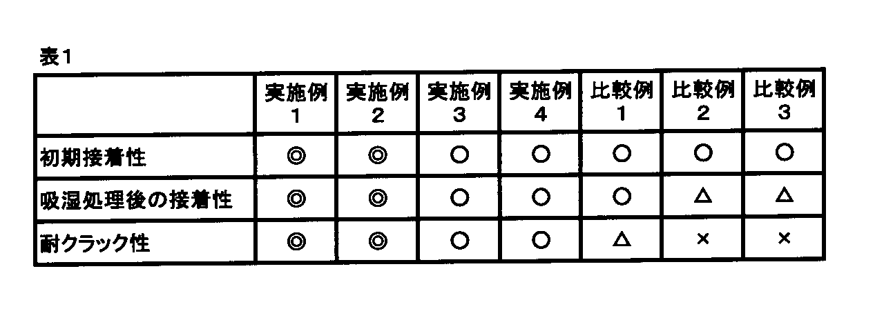
表1から明らかなように、実施例1〜4は、接着性に優れ、かつ耐クラック性にも優れていた。 As is clear from Table 1, Examples 1 to 4 were excellent in adhesion and crack resistance.
本発明の半導体用接着フィルムは、半導体素子とリードフレーム、有機基板等の半導体素子搭載用支持部材とを低温で接着することができ、かつ高温密着性も優れており、LOC構造やチップの上にチップを多段で積層する多層構造の半導体装置等に好適に用いることができる。 The adhesive film for a semiconductor of the present invention can bond a semiconductor element and a support member for mounting a semiconductor element such as a lead frame or an organic substrate at a low temperature, and has excellent high-temperature adhesion. It can be suitably used for a semiconductor device having a multilayer structure in which chips are stacked in multiple stages.
Claims (6)
Priority Applications (1)
| Application Number | Priority Date | Filing Date | Title |
|---|---|---|---|
| JP2004106274A JP2005290171A (en) | 2004-03-31 | 2004-03-31 | Adhesive film for semiconductor and semiconductor device |
Applications Claiming Priority (1)
| Application Number | Priority Date | Filing Date | Title |
|---|---|---|---|
| JP2004106274A JP2005290171A (en) | 2004-03-31 | 2004-03-31 | Adhesive film for semiconductor and semiconductor device |
Publications (1)
| Publication Number | Publication Date |
|---|---|
| JP2005290171A true JP2005290171A (en) | 2005-10-20 |
Family
ID=35323476
Family Applications (1)
| Application Number | Title | Priority Date | Filing Date |
|---|---|---|---|
| JP2004106274A Pending JP2005290171A (en) | 2004-03-31 | 2004-03-31 | Adhesive film for semiconductor and semiconductor device |
Country Status (1)
| Country | Link |
|---|---|
| JP (1) | JP2005290171A (en) |
Cited By (1)
| Publication number | Priority date | Publication date | Assignee | Title |
|---|---|---|---|---|
| JP2009256588A (en) * | 2008-03-26 | 2009-11-05 | Hitachi Chem Co Ltd | Film-like adhesive for sealing semiconductor, semiconductor device, and its manufacturing method |
Citations (6)
| Publication number | Priority date | Publication date | Assignee | Title |
|---|---|---|---|---|
| JPH04189885A (en) * | 1990-04-26 | 1992-07-08 | Nippon Carbide Ind Co Inc | Thermosetting pressure-sensitive adhesive composition and thermosetting pressure-sensitive adhesive sheet |
| JPH07300577A (en) * | 1993-09-20 | 1995-11-14 | Cheil Synthetics Inc | Adhesive composition for flexible printed circuit substrate |
| JP2002322457A (en) * | 2001-04-26 | 2002-11-08 | Tomoegawa Paper Co Ltd | Adhesive composition for semiconductor device and adhesive sheet for semiconductor device |
| JP2003206464A (en) * | 2002-01-15 | 2003-07-22 | Hitachi Chem Co Ltd | Adhesive composition, adhesive film, wiring board for mounting semiconductor, semiconductor device and method of manufacturing the same |
| JP2003286391A (en) * | 2002-03-28 | 2003-10-10 | Nippon Steel Chem Co Ltd | Epoxy resin composition, varnish, film adhesive using this epoxy resin composition, and cured product thereof |
| JP2004099833A (en) * | 2002-09-12 | 2004-04-02 | Three M Innovative Properties Co | Thermosetting adhesive composition, film adhesive, and semiconductor device |
-
2004
- 2004-03-31 JP JP2004106274A patent/JP2005290171A/en active Pending
Patent Citations (6)
| Publication number | Priority date | Publication date | Assignee | Title |
|---|---|---|---|---|
| JPH04189885A (en) * | 1990-04-26 | 1992-07-08 | Nippon Carbide Ind Co Inc | Thermosetting pressure-sensitive adhesive composition and thermosetting pressure-sensitive adhesive sheet |
| JPH07300577A (en) * | 1993-09-20 | 1995-11-14 | Cheil Synthetics Inc | Adhesive composition for flexible printed circuit substrate |
| JP2002322457A (en) * | 2001-04-26 | 2002-11-08 | Tomoegawa Paper Co Ltd | Adhesive composition for semiconductor device and adhesive sheet for semiconductor device |
| JP2003206464A (en) * | 2002-01-15 | 2003-07-22 | Hitachi Chem Co Ltd | Adhesive composition, adhesive film, wiring board for mounting semiconductor, semiconductor device and method of manufacturing the same |
| JP2003286391A (en) * | 2002-03-28 | 2003-10-10 | Nippon Steel Chem Co Ltd | Epoxy resin composition, varnish, film adhesive using this epoxy resin composition, and cured product thereof |
| JP2004099833A (en) * | 2002-09-12 | 2004-04-02 | Three M Innovative Properties Co | Thermosetting adhesive composition, film adhesive, and semiconductor device |
Cited By (1)
| Publication number | Priority date | Publication date | Assignee | Title |
|---|---|---|---|---|
| JP2009256588A (en) * | 2008-03-26 | 2009-11-05 | Hitachi Chem Co Ltd | Film-like adhesive for sealing semiconductor, semiconductor device, and its manufacturing method |
Similar Documents
| Publication | Publication Date | Title |
|---|---|---|
| KR101058659B1 (en) | Semiconductor film, manufacturing method of semiconductor film and semiconductor device | |
| WO2010044179A1 (en) | Method for manufacturing semiconductor device and semiconductor device | |
| WO2009113296A1 (en) | Resin varnish for semiconductor element bonding film formation, semiconductor element bonding film, and semiconductor device | |
| JP5115096B2 (en) | Adhesive film | |
| JP2011018806A (en) | Film for semiconductor, and method of manufacturing semiconductor device | |
| JP3754700B1 (en) | Adhesive film for semiconductor and semiconductor device using the same | |
| JP4893640B2 (en) | Adhesive film for semiconductor and semiconductor device using the same | |
| JP4303705B2 (en) | Adhesive film for semiconductor and semiconductor device using the same | |
| JP4380684B2 (en) | Adhesive film for semiconductor, dicing film and semiconductor device | |
| JP4309710B2 (en) | Adhesive film for semiconductor, dicing film and semiconductor device | |
| JP2008211224A (en) | Die attach film with dicing sheet function and method for manufacturing semiconductor device using the same | |
| JP2006269887A (en) | Adhesive film for semiconductor and semiconductor device using the same | |
| JP4319108B2 (en) | Adhesive film for semiconductor and semiconductor device | |
| JP2006165074A (en) | Die attach film with dicing sheet function and method for manufacturing semiconductor device using the same | |
| JP4466397B2 (en) | Adhesive film for semiconductor and semiconductor device using the same | |
| JP4050290B2 (en) | Adhesive film for semiconductor and semiconductor device using the same | |
| JP2005203401A (en) | Semiconductor device manufacturing method and semiconductor device | |
| JP4400609B2 (en) | Adhesive film for semiconductor and semiconductor device | |
| JP5003090B2 (en) | Adhesive film and semiconductor device using the same | |
| JP5564782B2 (en) | Adhesive composition, film adhesive, adhesive sheet and semiconductor device | |
| JP2008300862A (en) | Adhesive film for semiconductor and semiconductor device | |
| JP3735106B2 (en) | Adhesive film for semiconductor and semiconductor device | |
| JP2006237483A (en) | A die attach film with a dicing sheet function, a method of manufacturing a semiconductor device using the same, and a semiconductor device. | |
| JP2006206787A (en) | A die attach film with a dicing sheet function, a method of manufacturing a semiconductor device using the same, and a semiconductor device. | |
| JP2005290171A (en) | Adhesive film for semiconductor and semiconductor device |
Legal Events
| Date | Code | Title | Description |
|---|---|---|---|
| A621 | Written request for application examination |
Free format text: JAPANESE INTERMEDIATE CODE: A621 Effective date: 20061027 |
|
| A977 | Report on retrieval |
Free format text: JAPANESE INTERMEDIATE CODE: A971007 Effective date: 20090611 |
|
| A131 | Notification of reasons for refusal |
Free format text: JAPANESE INTERMEDIATE CODE: A131 Effective date: 20090616 |
|
| A521 | Written amendment |
Free format text: JAPANESE INTERMEDIATE CODE: A523 Effective date: 20090817 |
|
| A131 | Notification of reasons for refusal |
Free format text: JAPANESE INTERMEDIATE CODE: A131 Effective date: 20091104 |
|
| A521 | Written amendment |
Free format text: JAPANESE INTERMEDIATE CODE: A523 Effective date: 20091225 |
|
| A131 | Notification of reasons for refusal |
Free format text: JAPANESE INTERMEDIATE CODE: A131 Effective date: 20100202 |
|
| A02 | Decision of refusal |
Free format text: JAPANESE INTERMEDIATE CODE: A02 Effective date: 20100601 |