JP2005294793A - 窒化物半導体発光素子及びその製造方法 - Google Patents
窒化物半導体発光素子及びその製造方法 Download PDFInfo
- Publication number
- JP2005294793A JP2005294793A JP2004212480A JP2004212480A JP2005294793A JP 2005294793 A JP2005294793 A JP 2005294793A JP 2004212480 A JP2004212480 A JP 2004212480A JP 2004212480 A JP2004212480 A JP 2004212480A JP 2005294793 A JP2005294793 A JP 2005294793A
- Authority
- JP
- Japan
- Prior art keywords
- nitride semiconductor
- semiconductor layer
- light emitting
- emitting device
- layer
- Prior art date
- Legal status (The legal status is an assumption and is not a legal conclusion. Google has not performed a legal analysis and makes no representation as to the accuracy of the status listed.)
- Granted
Links
Images
Classifications
-
- H—ELECTRICITY
- H10—SEMICONDUCTOR DEVICES; ELECTRIC SOLID-STATE DEVICES NOT OTHERWISE PROVIDED FOR
- H10H—INORGANIC LIGHT-EMITTING SEMICONDUCTOR DEVICES HAVING POTENTIAL BARRIERS
- H10H20/00—Individual inorganic light-emitting semiconductor devices having potential barriers, e.g. light-emitting diodes [LED]
- H10H20/01—Manufacture or treatment
- H10H20/011—Manufacture or treatment of bodies, e.g. forming semiconductor layers
- H10H20/013—Manufacture or treatment of bodies, e.g. forming semiconductor layers having light-emitting regions comprising only Group III-V materials
- H10H20/0137—Manufacture or treatment of bodies, e.g. forming semiconductor layers having light-emitting regions comprising only Group III-V materials the light-emitting regions comprising nitride materials
-
- F—MECHANICAL ENGINEERING; LIGHTING; HEATING; WEAPONS; BLASTING
- F21—LIGHTING
- F21V—FUNCTIONAL FEATURES OR DETAILS OF LIGHTING DEVICES OR SYSTEMS THEREOF; STRUCTURAL COMBINATIONS OF LIGHTING DEVICES WITH OTHER ARTICLES, NOT OTHERWISE PROVIDED FOR
- F21V7/00—Reflectors for light sources
- F21V7/0008—Reflectors for light sources providing for indirect lighting
-
- F—MECHANICAL ENGINEERING; LIGHTING; HEATING; WEAPONS; BLASTING
- F21—LIGHTING
- F21S—NON-PORTABLE LIGHTING DEVICES; SYSTEMS THEREOF; VEHICLE LIGHTING DEVICES SPECIALLY ADAPTED FOR VEHICLE EXTERIORS
- F21S8/00—Lighting devices intended for fixed installation
- F21S8/08—Lighting devices intended for fixed installation with a standard
- F21S8/085—Lighting devices intended for fixed installation with a standard of high-built type, e.g. street light
-
- F—MECHANICAL ENGINEERING; LIGHTING; HEATING; WEAPONS; BLASTING
- F21—LIGHTING
- F21V—FUNCTIONAL FEATURES OR DETAILS OF LIGHTING DEVICES OR SYSTEMS THEREOF; STRUCTURAL COMBINATIONS OF LIGHTING DEVICES WITH OTHER ARTICLES, NOT OTHERWISE PROVIDED FOR
- F21V29/00—Protecting lighting devices from thermal damage; Cooling or heating arrangements specially adapted for lighting devices or systems
- F21V29/50—Cooling arrangements
- F21V29/60—Cooling arrangements characterised by the use of a forced flow of gas, e.g. air
- F21V29/67—Cooling arrangements characterised by the use of a forced flow of gas, e.g. air characterised by the arrangement of fans
-
- H—ELECTRICITY
- H10—SEMICONDUCTOR DEVICES; ELECTRIC SOLID-STATE DEVICES NOT OTHERWISE PROVIDED FOR
- H10P—GENERIC PROCESSES OR APPARATUS FOR THE MANUFACTURE OR TREATMENT OF DEVICES COVERED BY CLASS H10
- H10P14/00—Formation of materials, e.g. in the shape of layers or pillars
- H10P14/20—Formation of materials, e.g. in the shape of layers or pillars of semiconductor materials
- H10P14/27—Formation of materials, e.g. in the shape of layers or pillars of semiconductor materials using selective deposition, e.g. simultaneous growth of monocrystalline and non-monocrystalline semiconductor materials
- H10P14/271—Formation of materials, e.g. in the shape of layers or pillars of semiconductor materials using selective deposition, e.g. simultaneous growth of monocrystalline and non-monocrystalline semiconductor materials characterised by the preparation of substrate for selective deposition
-
- H—ELECTRICITY
- H10—SEMICONDUCTOR DEVICES; ELECTRIC SOLID-STATE DEVICES NOT OTHERWISE PROVIDED FOR
- H10P—GENERIC PROCESSES OR APPARATUS FOR THE MANUFACTURE OR TREATMENT OF DEVICES COVERED BY CLASS H10
- H10P14/00—Formation of materials, e.g. in the shape of layers or pillars
- H10P14/20—Formation of materials, e.g. in the shape of layers or pillars of semiconductor materials
- H10P14/27—Formation of materials, e.g. in the shape of layers or pillars of semiconductor materials using selective deposition, e.g. simultaneous growth of monocrystalline and non-monocrystalline semiconductor materials
- H10P14/276—Lateral overgrowth
-
- H—ELECTRICITY
- H10—SEMICONDUCTOR DEVICES; ELECTRIC SOLID-STATE DEVICES NOT OTHERWISE PROVIDED FOR
- H10P—GENERIC PROCESSES OR APPARATUS FOR THE MANUFACTURE OR TREATMENT OF DEVICES COVERED BY CLASS H10
- H10P14/00—Formation of materials, e.g. in the shape of layers or pillars
- H10P14/20—Formation of materials, e.g. in the shape of layers or pillars of semiconductor materials
- H10P14/29—Formation of materials, e.g. in the shape of layers or pillars of semiconductor materials characterised by the substrates
- H10P14/2901—Materials
- H10P14/2907—Materials being Group IIIA-VA materials
- H10P14/2908—Nitrides
-
- H—ELECTRICITY
- H10—SEMICONDUCTOR DEVICES; ELECTRIC SOLID-STATE DEVICES NOT OTHERWISE PROVIDED FOR
- H10P—GENERIC PROCESSES OR APPARATUS FOR THE MANUFACTURE OR TREATMENT OF DEVICES COVERED BY CLASS H10
- H10P14/00—Formation of materials, e.g. in the shape of layers or pillars
- H10P14/20—Formation of materials, e.g. in the shape of layers or pillars of semiconductor materials
- H10P14/32—Formation of materials, e.g. in the shape of layers or pillars of semiconductor materials characterised by intermediate layers between substrates and deposited layers
- H10P14/3202—Materials thereof
- H10P14/3214—Materials thereof being Group IIIA-VA semiconductors
- H10P14/3216—Nitrides
-
- H—ELECTRICITY
- H10—SEMICONDUCTOR DEVICES; ELECTRIC SOLID-STATE DEVICES NOT OTHERWISE PROVIDED FOR
- H10P—GENERIC PROCESSES OR APPARATUS FOR THE MANUFACTURE OR TREATMENT OF DEVICES COVERED BY CLASS H10
- H10P14/00—Formation of materials, e.g. in the shape of layers or pillars
- H10P14/20—Formation of materials, e.g. in the shape of layers or pillars of semiconductor materials
- H10P14/34—Deposited materials, e.g. layers
- H10P14/3402—Deposited materials, e.g. layers characterised by the chemical composition
- H10P14/3414—Deposited materials, e.g. layers characterised by the chemical composition being group IIIA-VIA materials
- H10P14/3416—Nitrides
-
- F—MECHANICAL ENGINEERING; LIGHTING; HEATING; WEAPONS; BLASTING
- F21—LIGHTING
- F21W—INDEXING SCHEME ASSOCIATED WITH SUBCLASSES F21K, F21L, F21S and F21V, RELATING TO USES OR APPLICATIONS OF LIGHTING DEVICES OR SYSTEMS
- F21W2131/00—Use or application of lighting devices or systems not provided for in codes F21W2102/00-F21W2121/00
- F21W2131/10—Outdoor lighting
- F21W2131/103—Outdoor lighting of streets or roads
Landscapes
- Engineering & Computer Science (AREA)
- General Engineering & Computer Science (AREA)
- Led Devices (AREA)
Abstract
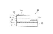
【解決手段】AlNから成る多結晶または非晶質基板(21)と、上記AlN基板(21)上に形成され、ストライプ形状または格子形状の複数個の誘電体パターン(23)と、上記誘電体パターン(23)の形成されたAlN基板(21)上に側面成長法により形成された側面成長窒化物半導体層(24)と、上記窒化物半導体層(24)上に形成された第1導電型窒化物半導体層(25)と、上記第1導電型窒化物半導体層(25)上に形成された活性層(26)と、上記活性層(26)上に形成された第2導電型窒化物半導体層(27)とを含む窒化物半導体発光素子(20)を提供する。
【選択図】図1
Description
32 バッファ層
33 誘電体パターン
34 側面成長窒化物半導体層
35 第1導電型窒化物半導体層
36 活性層
37 第2導電型窒化物半導体層
38 透明電極層
39a、39b 第1及び第2電極
Claims (22)
- AlNから成る多結晶または非晶質基板と、
上記AlN基板上に形成され、ストライプ状または格子状の複数個の誘電体パターンと、
上記誘電体パターンの形成されたAlN基板上に側面成長法により形成された側面成長窒化物半導体層と、
上記窒化物半導体層上に形成された第1導電型窒化物半導体層と、
上記第1導電型窒化物半導体層上に形成された活性層と、
上記活性層上に形成された第2導電型窒化物半導体層と、
を有することを特徴とする窒化物半導体発光素子。 - 上記AlN基板は多結晶基板で、上記AlN多結晶基板は所定の面方向を有する凹凸の形成された上面を有することを特徴とする請求項1に記載の窒化物半導体発光素子。
- 上記AlN基板上に形成されたバッファ層をさらに有することを特徴とする請求項1に記載の窒化物半導体発光素子。
- 上記バッファ層はAlxGa1−xN(0≦x≦1)の物質から成る低温核成長層であることを特徴とする請求項3に記載の窒化物半導体発光素子。
- 上記バッファ層は所定の面方向を有する凹凸の形成された上面を有することを特徴とする請求項3に記載の窒化物半導体発光素子。
- 上記誘電体パターンはSiO2またはSiNから成ることを特徴とする請求項1に記載の窒化物半導体発光素子。
- 上記側面成長窒化物半導体層は第1導電型不純物を含む窒化物半導体層であることを特徴とする請求項1に記載の窒化物半導体発光素子。
- 上記第1導電型窒化物半導体層はn型窒化物半導体層で、上記第2導電型窒化物半導体層はp型窒化物半導体層であることを特徴とする請求項1に記載の窒化物半導体発光素子。
- 上記基板はGa及びIn中少なくとも一つの元素をさらに含む(GaIn)AlN基板であることを特徴とする請求項1に記載の窒化物半導体発光素子。
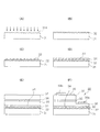
- AlNから成る多結晶または非晶質基板を用意する段階と、
上記AlN基板上にストライプ状または格子状の複数個の誘電体パターンを形成する段階と、
上記誘電体パターンの形成されたAlN基板上に側面成長法を利用して側面成長窒化物半導体層を形成する段階と、
上記窒化物半導体層上に第1導電型窒化物半導体層を形成する段階と、
上記第1導電型窒化物半導体層上に活性層を形成する段階と、
上記活性層上に第2導電型窒化物半導体層を形成する段階と、
を有することを特徴とする窒化物半導体発光素子の製造方法。 - 上記AlN基板は多結晶基板で、上記AlN多結晶基板上に所定の面方向を有する凹凸が形成されるよう、上記AlN基板上面をエッチングする段階をさらに有することを特徴とする請求項10に記載の窒化物半導体発光素子の製造方法。
- 上記エッチングする段階はAlN基板上にNaOHを含むエッチング液を利用して湿式エッチングを適用する段階であることを特徴とする請求項11に記載の窒化物半導体発光素子の製造方法。
- 上記誘電体パターンを形成する段階前に、AlN基板上にバッファ層を形成する段階をさらに有することを特徴とする請求項10に記載の窒化物半導体発光素子の製造方法。
- 上記バッファ層はAlxGa1−xN(0≦x≦1)の物質から成る低温核成長層であることを特徴とする請求項13に記載の窒化物半導体発光素子の製造方法。
- 上記バッファ層上に所定の面方向を有する凹凸が形成されるよう、上記バッファ層上面をエッチングする段階をさらに有することを特徴とする請求項13に記載の窒化物半導体発光素子の製造方法。
- 上記エッチングする段階は、上記バッファ層上にNaOHを含むエッチング液を利用して湿式エッチングを適用する段階であることを特徴とする請求項15に記載の窒化物半導体発光素子の製造方法。
- 上記誘電体パターンはSiO2またはSiNから成ることを特徴とする請求項10に記載の窒化物半導体発光素子製造方法。
- 上記側面成長窒化物半導体層は第1導電型不純物を含んだ窒化物半導体層であることを特徴とする請求項10に記載の窒化物半導体発光素子の製造方法。
- 上記第1導電型窒化物半導体層はn型窒化物半導体層で、上記第2導電型窒化物半導体層はp型窒化物半導体層であることを特徴とする請求項10に記載の窒化物半導体発光素子の製造方法。
- 上記側面成長窒化物半導体層はAlを含んだ窒化物半導体層で、
上記側面成長窒化物半導体層を形成する段階は、
Cl系ガスまたはBr系ガスを注入しながら、側面成長法を利用して上記側面成長窒化物半導体層を形成する段階であることを特徴とする請求項10に記載の窒化物半導体発光素子の製造方法。 - 上記Br系ガスまたは上記Cl系ガスは、
Br2、Cl2、CBr4、CCl4、HBr及びHClから構成された群から選択された少なくとも一種を含むガスであることを特徴とする請求項20に記載の窒化物半導体発光素子の製造方法。 - 上記基板はGa及びIn中少なくとも一つの元素をさらに含む(GaIn)AlN基板であることを特徴とする請求項10に記載の窒化物半導体発光素子の製造方法。
Applications Claiming Priority (1)
| Application Number | Priority Date | Filing Date | Title |
|---|---|---|---|
| KR20040021906A KR100568300B1 (ko) | 2004-03-31 | 2004-03-31 | 질화물 반도체 발광소자 및 그 제조방법 |
Publications (2)
| Publication Number | Publication Date |
|---|---|
| JP2005294793A true JP2005294793A (ja) | 2005-10-20 |
| JP4048191B2 JP4048191B2 (ja) | 2008-02-13 |
Family
ID=35053327
Family Applications (1)
| Application Number | Title | Priority Date | Filing Date |
|---|---|---|---|
| JP2004212480A Expired - Fee Related JP4048191B2 (ja) | 2004-03-31 | 2004-07-21 | 窒化物半導体発光素子及びその製造方法 |
Country Status (3)
| Country | Link |
|---|---|
| US (2) | US8664687B2 (ja) |
| JP (1) | JP4048191B2 (ja) |
| KR (1) | KR100568300B1 (ja) |
Cited By (4)
| Publication number | Priority date | Publication date | Assignee | Title |
|---|---|---|---|---|
| JP2012048862A (ja) * | 2010-08-24 | 2012-03-08 | Stanley Electric Co Ltd | 車両用灯具 |
| JPWO2010100942A1 (ja) * | 2009-03-05 | 2012-09-06 | 株式会社小糸製作所 | 発光モジュール、発光モジュールの製造方法、および灯具ユニット |
| KR101855063B1 (ko) * | 2011-06-24 | 2018-05-04 | 엘지이노텍 주식회사 | 발광 소자 |
| JP2018080103A (ja) * | 2010-12-14 | 2018-05-24 | ヘクサテック,インコーポレイテッド | 多結晶質窒化アルミニウム焼結体の熱膨張処理、および半導体製造へのその応用 |
Families Citing this family (27)
| Publication number | Priority date | Publication date | Assignee | Title |
|---|---|---|---|---|
| KR100649494B1 (ko) * | 2004-08-17 | 2006-11-24 | 삼성전기주식회사 | 레이저를 이용하여 발광 다이오드 기판을 표면 처리하는발광 다이오드 제조 방법 및 이 방법에 의해 제조된 발광다이오드 |
| KR100664988B1 (ko) | 2004-11-04 | 2007-01-09 | 삼성전기주식회사 | 광추출효율이 향상된 반도체 발광소자 |
| US20070145386A1 (en) | 2004-12-08 | 2007-06-28 | Samsung Electro-Mechanics Co., Ltd. | Semiconductor light emitting device and method of manufacturing the same |
| KR100887067B1 (ko) * | 2006-02-14 | 2009-03-04 | 삼성전기주식회사 | 나노 패턴 구조를 지닌 반도체 발광 소자의 제조 방법 |
| KR100624449B1 (ko) | 2004-12-08 | 2006-09-18 | 삼성전기주식회사 | 요철 구조를 포함하는 발광 소자 및 그 제조 방법 |
| EP2259318A3 (en) * | 2005-02-04 | 2014-01-08 | Seoul Opto Device Co., Ltd. | Light emitting device having a plurality of light emitting cells and method of fabricating the same |
| KR100669142B1 (ko) * | 2005-04-20 | 2007-01-15 | (주)더리즈 | 발광 소자와 이의 제조 방법 |
| KR100715011B1 (ko) * | 2005-12-15 | 2007-05-09 | 서울옵토디바이스주식회사 | 버퍼층이 형성된 발광소자와 그의 제조방법 |
| KR100659373B1 (ko) * | 2006-02-09 | 2006-12-19 | 서울옵토디바이스주식회사 | 패터닝된 발광다이오드용 기판 및 그것을 채택하는 발광다이오드 |
| KR20070081184A (ko) | 2006-02-10 | 2007-08-16 | 삼성전기주식회사 | 질화물계 반도체 발광소자 및 그 제조방법 |
| KR100820836B1 (ko) * | 2006-09-12 | 2008-04-11 | 엘지전자 주식회사 | 발광 다이오드 제조방법 |
| DE102006043400A1 (de) * | 2006-09-15 | 2008-03-27 | Osram Opto Semiconductors Gmbh | Optoelektronischer Halbleiterchip |
| KR100836455B1 (ko) * | 2007-01-11 | 2008-06-09 | 엘지이노텍 주식회사 | 반도체 발광소자 및 반도체 발광소자의 제조 방법 |
| KR100893188B1 (ko) * | 2007-03-13 | 2009-04-16 | 삼성전기주식회사 | 질화물계 반도체 발광소자 및 그 제조방법 |
| KR100892664B1 (ko) * | 2007-06-29 | 2009-04-15 | 서울옵토디바이스주식회사 | 수직형 발광 다이오드와 그 제조 방법 및 이를 구비한 발광다이오드 |
| KR100974048B1 (ko) * | 2008-02-19 | 2010-08-04 | 우리엘에스티 주식회사 | 하이브리드 버퍼층을 이용한 질화물 반도체 발광소자 및이의 제조방법 |
| KR100988146B1 (ko) | 2008-07-16 | 2010-10-18 | 주식회사 실트론 | 화합물 반도체 기판, 그 제조 방법 및 이를 이용한 화합물반도체 소자 |
| KR20100030472A (ko) | 2008-09-10 | 2010-03-18 | 삼성전자주식회사 | 발광 소자 및 발광 장치의 제조 방법, 상기 방법을 이용하여 제조한 발광 소자 및 발광 장치 |
| KR101125397B1 (ko) * | 2009-10-20 | 2012-04-02 | 엘지이노텍 주식회사 | 반도체 발광소자 및 그 제조방법 |
| KR101007087B1 (ko) | 2009-10-26 | 2011-01-10 | 엘지이노텍 주식회사 | 발광소자 및 그 제조방법 |
| CN103003920B (zh) * | 2010-09-27 | 2016-09-14 | 株式会社东芝 | GaN基半导体结晶成长用多晶氮化铝基材及使用该基材的GaN基半导体的制造方法 |
| TWI480926B (zh) * | 2010-09-28 | 2015-04-11 | 國立中興大學 | Preparation method of epitaxial element |
| CN102610717B (zh) * | 2011-01-20 | 2015-02-25 | 赛恩倍吉科技顾问(深圳)有限公司 | 半导体发光芯片及其制造方法 |
| KR101407698B1 (ko) * | 2012-12-28 | 2014-06-16 | 한국광기술원 | 질화물계 반도체 소자 및 그의 제조 방법 |
| US9112101B2 (en) * | 2013-04-25 | 2015-08-18 | Epistar Corporation | Light-emitting device manufacturing method |
| CN103545412A (zh) * | 2013-10-30 | 2014-01-29 | 华南理工大学 | 一种具有混合图案的led图形优化衬底及led芯片 |
| KR102328457B1 (ko) | 2015-05-29 | 2021-11-18 | 쑤저우 레킨 세미컨덕터 컴퍼니 리미티드 | 발광소자, 발광소자 제조방법 및 이를 구비하는 조명시스템 |
Family Cites Families (22)
| Publication number | Priority date | Publication date | Assignee | Title |
|---|---|---|---|---|
| JP3142312B2 (ja) * | 1991-07-30 | 2001-03-07 | 株式会社東芝 | 六方晶半導体の結晶成長方法 |
| JP3761935B2 (ja) | 1994-09-19 | 2006-03-29 | 株式会社東芝 | 化合物半導体装置 |
| JP3410863B2 (ja) | 1995-07-12 | 2003-05-26 | 株式会社東芝 | 化合物半導体装置及び化合物半導体発光装置 |
| JPH0936427A (ja) | 1995-07-18 | 1997-02-07 | Showa Denko Kk | 半導体装置及びその製造方法 |
| US6348096B1 (en) * | 1997-03-13 | 2002-02-19 | Nec Corporation | Method for manufacturing group III-V compound semiconductors |
| JP3898798B2 (ja) * | 1997-05-27 | 2007-03-28 | シャープ株式会社 | 窒化ガリウム系化合物半導体発光素子の製造方法 |
| US6091083A (en) * | 1997-06-02 | 2000-07-18 | Sharp Kabushiki Kaisha | Gallium nitride type compound semiconductor light-emitting device having buffer layer with non-flat surface |
| JP4032538B2 (ja) * | 1998-11-26 | 2008-01-16 | ソニー株式会社 | 半導体薄膜および半導体素子の製造方法 |
| JP3889910B2 (ja) | 2000-03-10 | 2007-03-07 | 三菱化学株式会社 | 半導体発光装置およびその製造方法 |
| JP3889911B2 (ja) | 2000-03-10 | 2007-03-07 | 三菱化学株式会社 | 半導体発光装置およびその製造方法 |
| JP3384782B2 (ja) * | 2000-03-16 | 2003-03-10 | 三洋電機株式会社 | 窒化物系半導体素子およびその製造方法 |
| US6841808B2 (en) * | 2000-06-23 | 2005-01-11 | Toyoda Gosei Co., Ltd. | Group III nitride compound semiconductor device and method for producing the same |
| JP3556916B2 (ja) * | 2000-09-18 | 2004-08-25 | 三菱電線工業株式会社 | 半導体基材の製造方法 |
| JP3679720B2 (ja) * | 2001-02-27 | 2005-08-03 | 三洋電機株式会社 | 窒化物系半導体素子および窒化物系半導体の形成方法 |
| JP2002261392A (ja) * | 2001-02-27 | 2002-09-13 | Sanyo Electric Co Ltd | 窒化物系半導体素子および窒化物系半導体の形成方法 |
| US6664560B2 (en) * | 2001-06-15 | 2003-12-16 | Cree, Inc. | Ultraviolet light emitting diode |
| JP3786054B2 (ja) | 2001-09-07 | 2006-06-14 | 日本電気株式会社 | 半導体光素子および半導体レーザ |
| US7105865B2 (en) * | 2001-09-19 | 2006-09-12 | Sumitomo Electric Industries, Ltd. | AlxInyGa1−x−yN mixture crystal substrate |
| US6724013B2 (en) | 2001-12-21 | 2004-04-20 | Xerox Corporation | Edge-emitting nitride-based laser diode with p-n tunnel junction current injection |
| JP3971192B2 (ja) | 2002-01-11 | 2007-09-05 | 株式会社アルバック | Cvd装置 |
| US7078735B2 (en) * | 2003-03-27 | 2006-07-18 | Sanyo Electric Co., Ltd. | Light-emitting device and illuminator |
| KR20050023540A (ko) * | 2003-08-28 | 2005-03-10 | 서울옵토디바이스주식회사 | 발광소자 |
-
2004
- 2004-03-31 KR KR20040021906A patent/KR100568300B1/ko not_active Expired - Fee Related
- 2004-07-21 JP JP2004212480A patent/JP4048191B2/ja not_active Expired - Fee Related
- 2004-07-26 US US10/898,204 patent/US8664687B2/en not_active Expired - Fee Related
-
2014
- 2014-01-10 US US14/152,980 patent/US20140127848A1/en not_active Abandoned
Cited By (4)
| Publication number | Priority date | Publication date | Assignee | Title |
|---|---|---|---|---|
| JPWO2010100942A1 (ja) * | 2009-03-05 | 2012-09-06 | 株式会社小糸製作所 | 発光モジュール、発光モジュールの製造方法、および灯具ユニット |
| JP2012048862A (ja) * | 2010-08-24 | 2012-03-08 | Stanley Electric Co Ltd | 車両用灯具 |
| JP2018080103A (ja) * | 2010-12-14 | 2018-05-24 | ヘクサテック,インコーポレイテッド | 多結晶質窒化アルミニウム焼結体の熱膨張処理、および半導体製造へのその応用 |
| KR101855063B1 (ko) * | 2011-06-24 | 2018-05-04 | 엘지이노텍 주식회사 | 발광 소자 |
Also Published As
| Publication number | Publication date |
|---|---|
| KR100568300B1 (ko) | 2006-04-05 |
| US20050218416A1 (en) | 2005-10-06 |
| JP4048191B2 (ja) | 2008-02-13 |
| KR20050096509A (ko) | 2005-10-06 |
| US8664687B2 (en) | 2014-03-04 |
| US20140127848A1 (en) | 2014-05-08 |
Similar Documents
| Publication | Publication Date | Title |
|---|---|---|
| JP4048191B2 (ja) | 窒化物半導体発光素子及びその製造方法 | |
| US6380051B1 (en) | Layered structure including a nitride compound semiconductor film and method for making the same | |
| JP3555500B2 (ja) | Iii族窒化物半導体及びその製造方法 | |
| JP5135501B2 (ja) | 窒化物単結晶基板の製造方法及びこれを利用した窒化物半導体発光素子の製造方法 | |
| JP4880456B2 (ja) | 窒素化合物系半導体装置およびその製造方法 | |
| JPWO2000004615A1 (ja) | 半導体レーザ、半導体装置及びその製造方法 | |
| JP4412827B2 (ja) | 窒化物半導体厚膜基板 | |
| JP2000353669A (ja) | 半導体基板およびその製造方法 | |
| JPH11135832A (ja) | 窒化ガリウム系化合物半導体及びその製造方法 | |
| KR20000035610A (ko) | 반도체 박막, 반도체 소자와 반도체 장치, 및 이들의 제조방법 | |
| CN102959739A (zh) | Iii族氮化物半导体器件及其制造方法 | |
| JP2007070154A (ja) | Iii−v族窒化物系半導体基板及びその製造方法 | |
| JPH11145057A (ja) | 窒化ガリウム系化合物半導体基板の製造方法 | |
| JPH11274082A (ja) | Iii 族窒化物半導体およびその製造方法、およびiii 族窒化物半導体装置 | |
| JP3841537B2 (ja) | 窒化ガリウム系化合物半導体及びその製造方法 | |
| JP4214859B2 (ja) | 窒化ガリウム(GaN)基板の製造方法 | |
| KR100616543B1 (ko) | 실리콘기판 상에 질화물 단결정성장방법, 이를 이용한질화물 반도체 발광소자 및 그 제조방법 | |
| JP4743989B2 (ja) | 半導体素子およびその製造方法ならびに半導体基板の製造方法 | |
| JP2002261394A (ja) | 窒化物系半導体素子および窒化物系半導体の形成方法 | |
| JP2003243702A (ja) | 半導体発光素子およびその製造方法 | |
| JP3883827B2 (ja) | 窒化物系半導体素子および窒化物系半導体の形成方法 | |
| JP4200115B2 (ja) | カーボンドープ半導体膜、半導体素子、及びこれらの製造方法 | |
| JPH09266355A (ja) | 半導体発光素子 | |
| JP4232326B2 (ja) | 低欠陥窒化物半導体の成長方法 | |
| JP2002289541A (ja) | GaN系半導体結晶の形成方法及びその結晶を用いたGaN系半導体素子の製造方法 |
Legal Events
| Date | Code | Title | Description |
|---|---|---|---|
| A131 | Notification of reasons for refusal |
Free format text: JAPANESE INTERMEDIATE CODE: A131 Effective date: 20070612 |
|
| A521 | Request for written amendment filed |
Free format text: JAPANESE INTERMEDIATE CODE: A523 Effective date: 20070911 |
|
| TRDD | Decision of grant or rejection written | ||
| A01 | Written decision to grant a patent or to grant a registration (utility model) |
Free format text: JAPANESE INTERMEDIATE CODE: A01 Effective date: 20071030 |
|
| A61 | First payment of annual fees (during grant procedure) |
Free format text: JAPANESE INTERMEDIATE CODE: A61 Effective date: 20071126 |
|
| FPAY | Renewal fee payment (event date is renewal date of database) |
Free format text: PAYMENT UNTIL: 20101130 Year of fee payment: 3 |
|
| R150 | Certificate of patent or registration of utility model |
Free format text: JAPANESE INTERMEDIATE CODE: R150 |
|
| FPAY | Renewal fee payment (event date is renewal date of database) |
Free format text: PAYMENT UNTIL: 20101130 Year of fee payment: 3 |
|
| FPAY | Renewal fee payment (event date is renewal date of database) |
Free format text: PAYMENT UNTIL: 20111130 Year of fee payment: 4 |
|
| S111 | Request for change of ownership or part of ownership |
Free format text: JAPANESE INTERMEDIATE CODE: R313113 |
|
| FPAY | Renewal fee payment (event date is renewal date of database) |
Free format text: PAYMENT UNTIL: 20111130 Year of fee payment: 4 |
|
| R360 | Written notification for declining of transfer of rights |
Free format text: JAPANESE INTERMEDIATE CODE: R360 |
|
| FPAY | Renewal fee payment (event date is renewal date of database) |
Free format text: PAYMENT UNTIL: 20111130 Year of fee payment: 4 |
|
| R370 | Written measure of declining of transfer procedure |
Free format text: JAPANESE INTERMEDIATE CODE: R370 |
|
| FPAY | Renewal fee payment (event date is renewal date of database) |
Free format text: PAYMENT UNTIL: 20111130 Year of fee payment: 4 |
|
| S111 | Request for change of ownership or part of ownership |
Free format text: JAPANESE INTERMEDIATE CODE: R313113 |
|
| FPAY | Renewal fee payment (event date is renewal date of database) |
Free format text: PAYMENT UNTIL: 20111130 Year of fee payment: 4 |
|
| R360 | Written notification for declining of transfer of rights |
Free format text: JAPANESE INTERMEDIATE CODE: R360 |
|
| FPAY | Renewal fee payment (event date is renewal date of database) |
Free format text: PAYMENT UNTIL: 20111130 Year of fee payment: 4 |
|
| FPAY | Renewal fee payment (event date is renewal date of database) |
Free format text: PAYMENT UNTIL: 20121130 Year of fee payment: 5 |
|
| FPAY | Renewal fee payment (event date is renewal date of database) |
Free format text: PAYMENT UNTIL: 20121130 Year of fee payment: 5 |
|
| S111 | Request for change of ownership or part of ownership |
Free format text: JAPANESE INTERMEDIATE CODE: R313111 |
|
| S631 | Written request for registration of reclamation of domicile |
Free format text: JAPANESE INTERMEDIATE CODE: R313631 |
|
| S111 | Request for change of ownership or part of ownership |
Free format text: JAPANESE INTERMEDIATE CODE: R313111 |
|
| S631 | Written request for registration of reclamation of domicile |
Free format text: JAPANESE INTERMEDIATE CODE: R313631 |
|
| S633 | Written request for registration of reclamation of name |
Free format text: JAPANESE INTERMEDIATE CODE: R313633 |
|
| FPAY | Renewal fee payment (event date is renewal date of database) |
Free format text: PAYMENT UNTIL: 20121130 Year of fee payment: 5 |
|
| R371 | Transfer withdrawn |
Free format text: JAPANESE INTERMEDIATE CODE: R371 |
|
| FPAY | Renewal fee payment (event date is renewal date of database) |
Free format text: PAYMENT UNTIL: 20121130 Year of fee payment: 5 |
|
| S111 | Request for change of ownership or part of ownership |
Free format text: JAPANESE INTERMEDIATE CODE: R313111 |
|
| S531 | Written request for registration of change of domicile |
Free format text: JAPANESE INTERMEDIATE CODE: R313531 |
|
| S533 | Written request for registration of change of name |
Free format text: JAPANESE INTERMEDIATE CODE: R313533 |
|
| R371 | Transfer withdrawn |
Free format text: JAPANESE INTERMEDIATE CODE: R371 |
|
| FPAY | Renewal fee payment (event date is renewal date of database) |
Free format text: PAYMENT UNTIL: 20131130 Year of fee payment: 6 |
|
| R350 | Written notification of registration of transfer |
Free format text: JAPANESE INTERMEDIATE CODE: R350 |
|
| LAPS | Cancellation because of no payment of annual fees |