JP2005294868A - Semiconductor device - Google Patents
Semiconductor device Download PDFInfo
- Publication number
- JP2005294868A JP2005294868A JP2005187403A JP2005187403A JP2005294868A JP 2005294868 A JP2005294868 A JP 2005294868A JP 2005187403 A JP2005187403 A JP 2005187403A JP 2005187403 A JP2005187403 A JP 2005187403A JP 2005294868 A JP2005294868 A JP 2005294868A
- Authority
- JP
- Japan
- Prior art keywords
- transistor
- circuit
- input
- cell
- channel
- Prior art date
- Legal status (The legal status is an assumption and is not a legal conclusion. Google has not performed a legal analysis and makes no representation as to the accuracy of the status listed.)
- Pending
Links
Images



Landscapes
- Semiconductor Integrated Circuits (AREA)
- Metal-Oxide And Bipolar Metal-Oxide Semiconductor Integrated Circuits (AREA)
Abstract
【課題】 この発明は、そのラッチアップ耐性を下げずに、入力用回路セルのサイズを小さくし、LSIのコストダウンを可能とする半導体装置を提供することを目的とする。
【解決手段】 この発明は、半導体集積回路のコア領域がCMOSで構成された半導体装置において、入力用回路セルの保護トランジスタ回路31(31B、31C)、41(41D、41E)が、Nチャネルトランジスタのみを用いて構成し、前記入力用回路セルを通った入力信号の初段のトランジスタ回路5は、内部コア領域に配置されている。
【選択図】 図4
An object of the present invention is to provide a semiconductor device capable of reducing the size of an input circuit cell and reducing the cost of an LSI without lowering the latch-up resistance.
In a semiconductor device in which a core region of a semiconductor integrated circuit is composed of CMOS, protection transistor circuits 31 (31B, 31C), 41 (41D, 41E) of input circuit cells are N-channel transistors. The first stage transistor circuit 5 of the input signal passing through the input circuit cell is disposed in the internal core region.
[Selection] Figure 4
Description
この発明は、サージ耐性やラッチアップ耐性を低下させずにチップ面積を小さくすることを可能とした半導体装置に関するものである。 The present invention relates to a semiconductor device capable of reducing a chip area without reducing surge resistance or latch-up resistance.
一般に、MOSトランジスタで構成される半導体装置は、一般に入力インピーダンスが高くなり、サージ耐性が弱いことが知られている。 In general, it is known that a semiconductor device composed of MOS transistors generally has high input impedance and weak surge resistance.
また、CMOSで構成される半導体装置においては、その構造上ラッチアップ耐性に弱いことが良く知られている。これはCMOS構造上存在する寄生PNPNサイリスタ構造が、何らかの原因、例えば、ノイズやサージ電圧等が印加されることをトリガーとしてオン状態になることで引き起こされる。 Further, it is well known that a semiconductor device composed of CMOS is weak in latch-up resistance due to its structure. This is caused by the parasitic PNPN thyristor structure existing on the CMOS structure being turned on for some reason, for example, application of noise or surge voltage.
そして、上記ラッチアップ現象及びその対策については、多くの特許公報等にも詳しく書かれている(例えば、特許文献1参照)。 The above latch-up phenomenon and countermeasures are also described in detail in many patent gazettes (see, for example, Patent Document 1).
上記サージ電圧などに対して、従来から取られている一般的対策として、保護対象となる半導体回路への入力や出力に保護回路を挿入することが行われている。すなわち、保護回路を入れることで、そのサージ電圧により発生する電流をクランプさせるものである。一般的な保護回路としては、特許文献2などに示されている。 As a general countermeasure conventionally taken against the surge voltage or the like, a protection circuit is inserted into an input or output to a semiconductor circuit to be protected. In other words, a current generated by the surge voltage is clamped by inserting a protection circuit. A general protection circuit is disclosed in Patent Document 2 and the like.
図1に一般的なCMOSの入力用回路セルの構成を示す。図1に示すように、CMOS入力用回路セルは、パッド1に接続される保護抵抗2、保護トランジスタ回路4、入力トランジスタ5と、保護抵抗2と入力トランジスタ5との間に設けられる保護トランジスタ回路3で構成されている。
FIG. 1 shows a configuration of a general CMOS input circuit cell. As shown in FIG. 1, the CMOS input circuit cell includes a protection resistor 2, a
入力トランジスタ回路5は、Pチャネルトランジスタ(Pch)5Gと、Nチャネルトランジスタ(Nch)5Hで構成され、入力パッド1から入力される信号が保護抵抗2を介して入力される。
The input transistor circuit 5 includes a P-channel transistor (Pch) 5G and an N-channel transistor (Nch) 5H, and a signal input from the
保護トランジスタ回路3は、Pチャネルトランジスタ(Pch)3Bと、Nチャネルトランジスタ(Nch)3C、保護トランジスタ回路4は、Pチャネルトランジスタ(Pch)4Dと、Nチャネルトランジスタ(Nch)4Eでそれぞれ構成されている。
The protection transistor circuit 3 includes a P-channel transistor (Pch) 3B and an N-channel transistor (Nch) 3C, and the
そして、パッド1から入力されてくるサージを吸収するために、この保護トランジスタ回路4のPチャネルトランジスタ(Pch)4DとNチャネルトランジスタ(Nch)4Eでは、それぞれ大きなサイズで形成されている。
In order to absorb the surge input from the
図2に従来の入力用回路セルにおける素子レイアウトを示す。図2において、aはNチャネルトランジスタの配置領域、bはPチャネルトランジスタの配置領域、cはラッチアップ耐性向上のためのPチャネルトランジスタとNチャネルトランジスタの隔離領域を示している。 FIG. 2 shows an element layout in a conventional input circuit cell. In FIG. 2, a is an N channel transistor arrangement region, b is a P channel transistor arrangement region, and c is an isolation region between the P channel transistor and the N channel transistor for improving latch-up resistance.
この図2に示すように、ラッチアップ耐性を上げるため、Pチャネルトランジスタ(Pch)4DとNチャネルトランジスタ(Nch)4Eはレイアウト上大きな距離をもって離れて配置されている。そして、PチャネルトランジスタとNチャネルトランジスタの隔離領域は、プロセスその他いろいろな要因にもよるが約60〜100ミクロン程度である。そしてこれは経験的、実験的に求められるのが通常である。 As shown in FIG. 2, in order to increase the latch-up resistance, the P-channel transistor (Pch) 4D and the N-channel transistor (Nch) 4E are arranged with a large distance in the layout. The isolation region between the P-channel transistor and the N-channel transistor is about 60 to 100 microns, depending on the process and various other factors. This is usually determined empirically and experimentally.
また、入力初段にある抵抗2はサージが印加された際に流れ込む電流量を絞ることが目的であり、結果的に次段の入力トランジスタ回路5(5G、5H)のゲート酸化膜の破壊を防いでいる。 The resistor 2 in the first input stage is intended to reduce the amount of current that flows when a surge is applied. As a result, the gate oxide film of the input transistor circuit 5 (5G, 5H) in the next stage is prevented from being destroyed. It is out.
そして、その入力初段となるトランジスタ5のトランジスタ長はデザインルールの最小サイズではなくサージによるゲート酸化膜破壊を防ぐために経験的に少し大きく設計されている。 The transistor length of the transistor 5 serving as the first input stage is designed not to be the minimum size of the design rule but to be a little larger empirically to prevent the gate oxide film from being destroyed by a surge.
図3に一般的なCMOSの出力用回路セルを示す。入力用回路セルと構成されているパーツは基本的に同じである。CMOS出力用回路セルは、パッド1に接続される保護抵抗2、保護トランジスタ回路3、出力トランジスタ回路4’とで構成されている。
FIG. 3 shows a general CMOS output circuit cell. The parts configured as the input circuit cell are basically the same. The CMOS output circuit cell includes a protective resistor 2, a protective transistor circuit 3, and an output transistor circuit 4 'connected to the
保護トランジスタ回路3’は、Pチャネルトランジスタ(Pch)3’Bと、Nチャネルトランジスタ(Nch)3’C、出力トランジスタ回路4’は、Pチャネルトランジスタ(Pch)4Dと、Nチャネルトランジスタ(Nch)4’Eでそれぞれ構成されている。
The protection transistor circuit 3 ′ includes a P-channel transistor (Pch) 3′B and an N-channel transistor (Nch) 3′C, and the
そして、図1、図3で気がつくところは、入力用回路セルの保護トランジスタ回路4は出力用回路セルの出力トランジスタ回路4’を使っているという点である。
1 and FIG. 3 is that the
その大きな理由は、一般にI/OセルはLSIの周囲に配置され、その端子が入力であろうと出力であろうと同じ高さで配置されることにある。近年LSIは自動配置配線ツールでレイアウトされるのが通常であり、内部マクロセル及びI/Oセルもその自動配置配線ツールで配置配線されるよう同じ高さで設計、レイアウトされている。 The main reason is that the I / O cells are generally arranged around the LSI, and the terminals are arranged at the same height whether they are input or output. In recent years, LSIs are usually laid out by an automatic placement and routing tool, and internal macro cells and I / O cells are designed and laid out at the same height so that they can be placed and routed by the automatic placement and routing tool.
そして、そのツールを使う以上、仮にI/Oセルの高さが小さいものが一部あったとしてもそこはデッド領域となり無意味となる。そして隣合わせのセルそれぞれの基本構成が違う場合ラッチアップを考慮する必要がある。 As long as the tool is used, even if there is a part of the I / O cell whose height is small, it becomes a dead area and is meaningless. When the basic configuration of each adjacent cell is different, it is necessary to consider latch-up.
また、サージ耐性を入力用回路セルと出力用回路セルと同様のレベルに保つためには同じパーツ、さらには同様のレイアウトにしておくことが無難である。そういったことから一般的にI/Oセルは入力であろうが出力であろうが同じ大きさになっていた。
ところで、上記した保護回路のサイズは相対的に大きくなってきている。また、ラッチアップ耐性の改善にはそのサージが印加されるところのPチャネルトランジスタ領域とNチャネルトランジスタ領域を大きく離して配置させることが単純かつ確実な方法として取られており、これらの理由により保護回路部の面積は大きくLSIの集積化、そしてチップサイズの縮小化の大きなさまたげになっていた。 By the way, the size of the protection circuit described above has become relatively large. In order to improve the latch-up resistance, the P-channel transistor region and the N-channel transistor region to which the surge is applied are arranged apart from each other as a simple and reliable method. The area of the circuit portion is large, which has been a great obstacle to LSI integration and chip size reduction.
また、特開平6−61433号公報に開示されているように、その保護回路中の保護ダイオードにショットキーダイオードを用いることにより、ラッチアップ耐性を上げるというものであり、これによれば正のサージパルスに対するラッチアップは大きく改善されるが、負のサージパルスによるそれにはまた対策が必要とされる。 Further, as disclosed in Japanese Patent Application Laid-Open No. 6-61433, by using a Schottky diode as a protection diode in the protection circuit, the latch-up resistance is increased. Although latch-up for pulses is greatly improved, measures against negative surge pulses also require countermeasures.
また、特開平7−211901号公報には、保護回路のソース部にコンデンサを設けることで、そのサージ印加のエネルギーを吸収しようとするものであるが、結果的にそのコンデンサは大容量が必要とされ、それを配置する領域が別途必要となり、LSIの集積化、そしてチップサイズの縮小化の大きなさまたげになっていた。 Japanese Patent Laid-Open No. 7-211901 tries to absorb the energy of surge application by providing a capacitor in the source part of the protection circuit, but as a result, the capacitor requires a large capacity. In addition, an area for arranging it is required separately, which is a great obstacle for LSI integration and chip size reduction.
また、今まで述べてきたこととは別に、入力用回路セル内の入力初段のトランジスタのサイズは、サージに対する耐圧を上げるため一般的に最小サイズよりは大き目のトランジスタ長で設計されていることもある。しかし、これはあくまで保護回路を入れた上での更なる安全策である。 Also, apart from what has been described so far, the size of the first input transistor in the input circuit cell is generally designed with a transistor length larger than the minimum size in order to increase the breakdown voltage against surge. is there. However, this is a further safety measure with a protection circuit.
しかしながら、上述したように、従来の保護回路の構成でそのラッチアップ耐性を上げるためには、Pチャネルトランジスタ領域とNチャネルトランジスタ領域の間を大きく空けてやる必要があり、LSIの集積化、そしてチップサイズの縮小化の大きなさまたげになるという問題があった。 However, as described above, in order to increase the latch-up resistance in the configuration of the conventional protection circuit, it is necessary to make a large space between the P-channel transistor region and the N-channel transistor region. There was a problem that the chip size was greatly reduced.
また、ショットキーダイオードを用いる場合もそれを追加してやる必要があり、そのトランジスタサイズは流せる電流量を考えた場合通常の保護ダイオードと同様のサイズが必要とされる。また、コンデンサを追加する方法も同様である。 Further, when a Schottky diode is used, it is necessary to add it, and the transistor size needs to be the same as that of a normal protection diode in consideration of the amount of current that can be passed. The method of adding a capacitor is the same.
このように、従来の方法ではラッチアップ耐性を下げずにその入力用回路セルの大きさを小さくすることは困難である。 Thus, it is difficult for the conventional method to reduce the size of the input circuit cell without lowering the latch-up resistance.
今日のLSIの微細化、高集積化にもかかわらず、その入力用回路セルの大きさがネックとなり低価格化に対応するための障害になっていた。 Despite the miniaturization and high integration of today's LSIs, the size of the input circuit cell has become a bottleneck and has become an obstacle to cope with lower prices.
上記問題点を解決するために、この発明は、そのラッチアップ耐性を下げずに、入力用回路セルのサイズを小さくし、LSIのコストダウンを可能とする半導体装置を提供することを目的とする。 In order to solve the above problems, an object of the present invention is to provide a semiconductor device capable of reducing the size of an input circuit cell and reducing the cost of an LSI without reducing the latch-up resistance. .
この発明は、半導体集積回路のコア領域がCMOSで構成された半導体装置において、入力用回路セルが、NチャネルまたはPチャネルのどちらか一方のトランジスタのみを用いて構成されていることを特徴とする。 The present invention is characterized in that, in a semiconductor device in which a core region of a semiconductor integrated circuit is constituted by CMOS, an input circuit cell is constituted by using only one of N-channel and P-channel transistors. .
前記入力用回路セルを通った入力信号の初段のトランジスタは、内部コア領域に配置され、前記初段のトランジスタは自動配置配線ツールでの配置が可能なように他のマクロセルと同じ高さに構成するとよい。 The first-stage transistor of the input signal that has passed through the input circuit cell is disposed in the internal core region, and the first-stage transistor is configured at the same height as other macrocells so that it can be placed by an automatic placement and routing tool. Good.
前記初段のトランジスタルは、DC特性を満たすようなPチャネルトランジスタまたはNチャネルトランジスタのトランジスタ比を用いるとともに、これらのトランジスタ長はデザインルールに従った最小サイズで書かれている内部のマクロセルより大きくするように構成するとよい。 The first-stage transistor uses a transistor ratio of a P-channel transistor or an N-channel transistor that satisfies DC characteristics, and these transistor lengths are made larger than the internal macrocell written in the minimum size according to the design rule. It may be configured as follows.
上記の構成によれば、半導体装置はラッチアップを考慮する必要がなくなるため、その回路セルを小さくすることができる。 According to the above configuration, since the semiconductor device does not need to consider latch-up, the circuit cell can be made small.
また、この発明は、NチャネルまたはPチャネルのどちらか一方のトランジスタのみを用いて構成された入力用回路セルからなる入力端子部を半導体チップの一辺に集めて配置することを特徴とする。 Further, the present invention is characterized in that input terminal portions composed of input circuit cells configured using only N-channel or P-channel transistors are gathered and arranged on one side of the semiconductor chip.
上記のように、NチャネルまたはPチャネルのどちらか一方のトランジスタのみを用いて構成された入力用回路セルからなる入力端子部を半導体チップの一辺に集めて配置することで、チップ面積を縮小することができ、安価な半導体装置を提供することができる。 As described above, the chip area is reduced by collecting and arranging the input terminal portions made up of input circuit cells using only one of the N-channel and P-channel transistors on one side of the semiconductor chip. Therefore, an inexpensive semiconductor device can be provided.
以上説明したように、この発明によれば、半導体装置はラッチアップを考慮する必要がなくなるため、その回路セルを小さくすることができる。 As described above, according to the present invention, the semiconductor device does not need to take latch-up into consideration, so that the circuit cell can be made small.
NチャネルまたはPチャネルのどちらか一方のトランジスタのみを用いて構成された入力用回路セルからなる入力端子部を半導体チップの一辺に集めて配置することで、チップ面積を縮小することができ、安価な半導体装置を提供することができる。 By collecting and arranging input terminal portions made up of input circuit cells using only N-channel or P-channel transistors on one side of the semiconductor chip, the chip area can be reduced and the cost is low. A semiconductor device can be provided.
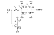
以下、この発明の実施の形態につき図面に従い説明する。図4は、この発明の実施の形態にかかる入力用回路セルの構成を示すブロック図である。 Embodiments of the present invention will be described below with reference to the drawings. FIG. 4 is a block diagram showing the configuration of the input circuit cell according to the embodiment of the present invention.
上記した図1の入力用回路セルと図3に示す出力用回路セルとから分かるように、CMOSの出力用回路セルと入力用回路セルと構成されているパーツは基本的に同じである。そして、図1、図3で気がつくところは、入力用回路セルの保護トランジスタ回路は出力用回路セルの出力トランジスタ回路を使っているという点である。一般的にI/Oセルは入力であろうが出力であろうが同じ大きさになっていた。 As can be seen from the input circuit cell shown in FIG. 1 and the output circuit cell shown in FIG. 3, the parts constituting the CMOS output circuit cell and the input circuit cell are basically the same. 1 and FIG. 3 is that the protection transistor circuit of the input circuit cell uses the output transistor circuit of the output circuit cell. In general, I / O cells have the same size whether they are input or output.
しかし、セルの機能を考えた場合、入力用回路セルに出力機能は必要とされず、すなわち、図1に示している大きなサイズの保護トランジスタ回路4は他に代用できるものがあれば削減可能である。そして、保護トランジスタ回路をPチャネルトランジスタが削減でき、Nチャネルだけで構成することが出来た場合、または、保護トランジスタ回路をNチャネルトランジスタが削減でき、Pチャネルだけで構成することが出来た場合、ラッチアップ耐性向上のために空けられていた大きな距離は必要なくなる。NチャネルトランジスタまたはPチャネルトランジスタだけの場合は、ラッチアップの原因であるサイリスタ構造になり得ないからである。
However, when considering the function of the cell, the output function is not required for the input circuit cell, that is, the
この発明は、上記したことを考慮してなされたものである。図4に示す実施形態では、保護トランジスタ回路をすべてNチャネルトランジスタで構成したものである。この実施形態における入力用回路セルは、パッド1に接続される保護抵抗2、Nチャネルトランジスタのみで構成された保護トランジスタ回路41、コア領域の一部となるCMOS入力トランジスタ5と、保護抵抗2と入力トランジスタ5との間に設けられるNチャネルトランジスタのみで構成された保護トランジスタ回路31で構成されている。
The present invention has been made in consideration of the above. In the embodiment shown in FIG. 4, all the protection transistor circuits are N-channel transistors. The input circuit cell in this embodiment includes a protection resistor 2 connected to the
上記のように、Nチャネルトランジスタのみで構成されているので、入力用回路セルは、ラッチアップ耐性向上のために空けられていた大きな距離(図2のc領域)は必要なくなる。 As described above, since it is composed of only N-channel transistors, the input circuit cell does not need the large distance (c region in FIG. 2) that is left for improving the latch-up resistance.
初段の入力トランジスタ回路5は、内部コア領域に配置され、初段の入力トランジスタ回路5は、自動配置配線ツールでの配置が可能なように内部コア領域に設けられる他のマクロセルと同じ高さに構成する The first-stage input transistor circuit 5 is arranged in the internal core region, and the first-stage input transistor circuit 5 is configured to be the same height as other macrocells provided in the internal core region so that the arrangement can be performed by the automatic placement and routing tool. Do
入力トランジスタ回路5は、DC特性を満たすようなNチャネルトランジスタのトランジスタ比を用いるとともに、これらのトランジスタ長はデザインルールに従った最小サイズで書かれている内部のマクロセルより大きくしている。 The input transistor circuit 5 uses transistor ratios of N-channel transistors that satisfy the DC characteristics, and the lengths of these transistors are larger than the internal macrocells written in the minimum size according to the design rule.
上記した入力用回路セルにおいて、パッド1に対Vcc+2kのサージ電圧が入力されると、保護トランジスタ回路31のトランジスタ31B、保護トランジスタ回路41のトランジスタ41Dにトランジスタオン電流が流れサージ電圧によるエネルギーを発散する。パッド1に対Vcc−2kのサージ電圧が入力されると、保護トランジスタ回路31のトランジスタ31B、保護トランジスタ回路4のトランジスタ41DにPN順方向電流が流れサージ電圧によるエネルギーを発散する。
In the above-described input circuit cell, when a surge voltage of Vcc + 2k is input to the
また、パッド1に対GND+2kのサージ電圧が入力されると、保護トランジスタ31のトランジスタ31C、保護トランジスタ回路41のトランジスタ41Eにパンチスルー電流が流れサージ電圧によるエネルギーを発散する。パッド1に対GND−2kのサージ電圧が入力されると、保護トランジスタ31のトランジスタ31C、保護トランジスタ回路41のトランジスタ41EにPN順方向電流が流れサージ電圧によるエネルギーを発散する。
In addition, when a surge voltage of GND + 2k is input to the
上記したように、入力用回路セルを用いた半導体装置はラッチアップを考慮する必要がなくなるためその入力用回路セルを小さくすることが可能となる。 As described above, since the semiconductor device using the input circuit cell does not need to consider latch-up, the input circuit cell can be made small.
図5に、この発明の第2の実施形態を示す。図5に示す実施形態では、保護トランジスタ回路をすべてPチャネルトランジスタで構成したものである。この実施形態における入力用回路セルは、パッド1に接続される保護抵抗2、Pチャネルトランジスタのみで構成された保護トランジスタ回路42、コア領域の一部となるCMOS入力トランジスタ回路5と、保護抵抗2と入力トランジスタ回路5との間に設けられるPチャネルトランジスタのみで構成された保護トランジスタ回路32で構成されている。
FIG. 5 shows a second embodiment of the present invention. In the embodiment shown in FIG. 5, all of the protection transistor circuits are P-channel transistors. The input circuit cell in this embodiment includes a protective resistor 2 connected to the
このように、保護トランジスタ回路をすべてPチャネルトランジスタで構成しても同様の効果が得られる。ただし、面積的には、保護トランジスタ回路をすべてNチャネルトランジスタで構成した場合よりも若干大きくなる。 In this way, the same effect can be obtained even if all the protection transistor circuits are P-channel transistors. However, in terms of area, the protection transistor circuit is slightly larger than when all the N-channel transistors are used.
今まで述べた保護トランジスタ31B、31C、41D、41Eは、通常のエンハンスメントトランジスタ以外に、必要に応じてフィールドトランジスタを用いてもよい。フィールドトランジスタの場合は、面積が少し大きくなることが予想されるが、パッド1から印加されるサージに対するトランジスタのゲート酸化膜耐圧が低いとき、フィールドトランジスタを用いることでその耐性を向上させる効果がある。
As the
次に、この発明による入力用回路セルを用いた場合と、図1に示す回路セルを用いた場合の半導体装置のチップ面積につき説明する。 Next, the chip area of the semiconductor device when the input circuit cell according to the present invention is used and when the circuit cell shown in FIG. 1 is used will be described.
図6は、図1、図3に示す従来のセルを用いた場合の半導体装置の構成図である。半導体チップ11に、ROM回路12,RAM回路13、ロジック回路14が配置される。チップ11の周囲には、図1,図3で示す構成のI/Oセル20が配置される。このI/Oセル20は、CMOSで構成されているため、図2に示すように、ラッチアップ耐性向上のためのPチャネル、Nチャネルトランジスタ隔離領域cが設けられており、その分面積が大きい。ROM回路12,RAM回路13へはI/Oセル20からそれぞれアドレス入力a,bが与えられる。ROM回路12からデータ出力cがI/Oセル20より出力される。RAM13、ロジック回路14は、データの入出力dがI/Oセル20を介して行われる。
FIG. 6 is a configuration diagram of a semiconductor device when the conventional cell shown in FIGS. 1 and 3 is used. A
上記のような構成においては、アドレス入力a,bは入力だけであるので、このI/Oセルをこの発明の入力用回路セルを用いることができる。そして、この発明の入力用回路セル21を半導体チップ11の一辺に集めて配置するとチップ面積を縮小することができる。図7は、この発明の入力用回路セルを用いた半導体装置の構成図である。この図7の例においては、左列の端子が全てアドレス入力という、入力用回路セルだけで構成できる。このため、この入力用回路セル21を図4に示す入力用回路セルで構成する。
In the configuration as described above, since the address inputs a and b are only inputs, the input circuit cell of the present invention can be used as this I / O cell. When the
なお、点線が示したものが、従来のI/Oセルを用いた場合の領域を示している。図7から分かるように、アドレス入力用の回路セルの大きさを半分以下にすることができ、一般的に、I/Oセルの大きさがチップ面積に示す割合が大きいので、この発明の入力用回路セルを用いるとチップ面積の縮小に大きく寄与することになる。 A dotted line indicates a region when a conventional I / O cell is used. As can be seen from FIG. 7, the size of the circuit cell for address input can be reduced to less than half, and generally the ratio of the size of the I / O cell to the chip area is large. Use of the circuit cell greatly contributes to the reduction of the chip area.
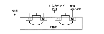
図8は、入力用回路セルをNチャネルトランジスタのみで構成した場合の断面図、図9は、入力用回路セルをPチャネルトランジスタのみで構成した場合の断面図である。図中矢印は、ラッチアップの要因になるため製品企画上認められていない電圧が入力された時の電流の流れを示している。 FIG. 8 is a cross-sectional view in the case where the input circuit cell is composed only of N-channel transistors, and FIG. 9 is a cross-sectional view in the case where the input circuit cell is composed only of P-channel transistors. The arrows in the figure indicate the current flow when a voltage that is not allowed in product planning is input because it causes latch-up.
Pチャネルトランジスタのみで構成した場合、入力用回路セルが全てPチャネルで構成されることで、セルのエリアには全てNウェルがひかれることになる。 In the case where only the P-channel transistor is used, all the input circuit cells are formed of the P-channel, so that all the N wells are drawn in the cell area.
実働作時、本来入力されるはずのない電圧、すなわち、電源電圧以上もしくはGND電圧以下の電圧が外来ノイズにより端子に入力される可能性がある。この場合保護トランジスタ回路が働き、サージを吸収する原理で電流が流れることになるが、このときNチャネルのみで構成した場合、あるいは従来のCMOSを用いた場合も同じであるが、その電流は基板を通っていくことになる。これは基板の電位を不安定にさせラッチアップの要因になり得る。 During actual operation, there is a possibility that a voltage that should not be input, that is, a voltage that is higher than the power supply voltage or lower than the GND voltage, is input to the terminal due to external noise. In this case, the protection transistor circuit works and current flows on the principle of absorbing surge. At this time, the current is also the same when the N-channel only is used or when a conventional CMOS is used. Will pass through. This can cause the substrate potential to become unstable and cause latch-up.
一方、図9に示すように、Pチャネルトランジスタのみで構成した場合、Nウェル中を電流が通るため、基板電位(P基板)への影響はない。また、このNウェルは、本来入力回路用セルにだけひかれているものであり、また、Nチャネルトランジスタは近くに存在しないため全くラッチアップの要因になり得ない。 On the other hand, as shown in FIG. 9, in the case where only the P-channel transistor is used, the current passes through the N well, so that the substrate potential (P substrate) is not affected. In addition, the N well is originally drawn only by the input circuit cell, and since the N channel transistor does not exist in the vicinity, it cannot cause a latch-up at all.
このように、Pチャネルトランジスタ構成する場合、面積を考えるとMOSの特性によりNチャネルトランジスタに対して大きくなるが、製品の信頼性という観点からPチャネルトランジスタを使用することも考慮できる。 As described above, when the P-channel transistor is configured, the area is larger than that of the N-channel transistor due to the characteristics of the MOS, but the use of the P-channel transistor can be considered from the viewpoint of product reliability.
1 パッド
2 保護抵抗
31 保護トランジスタ回路
41 保護トランジスタ回路
5 コア領域の一部となるCMOS入力トランジスタ回路
DESCRIPTION OF
Claims (1)
Priority Applications (1)
| Application Number | Priority Date | Filing Date | Title |
|---|---|---|---|
| JP2005187403A JP2005294868A (en) | 2005-06-27 | 2005-06-27 | Semiconductor device |
Applications Claiming Priority (1)
| Application Number | Priority Date | Filing Date | Title |
|---|---|---|---|
| JP2005187403A JP2005294868A (en) | 2005-06-27 | 2005-06-27 | Semiconductor device |
Related Parent Applications (1)
| Application Number | Title | Priority Date | Filing Date |
|---|---|---|---|
| JP2001278339A Division JP2003086707A (en) | 2001-09-13 | 2001-09-13 | Semiconductor device |
Publications (1)
| Publication Number | Publication Date |
|---|---|
| JP2005294868A true JP2005294868A (en) | 2005-10-20 |
Family
ID=35327376
Family Applications (1)
| Application Number | Title | Priority Date | Filing Date |
|---|---|---|---|
| JP2005187403A Pending JP2005294868A (en) | 2005-06-27 | 2005-06-27 | Semiconductor device |
Country Status (1)
| Country | Link |
|---|---|
| JP (1) | JP2005294868A (en) |
Citations (10)
| Publication number | Priority date | Publication date | Assignee | Title |
|---|---|---|---|---|
| JPS59167036A (en) * | 1983-03-14 | 1984-09-20 | Nec Corp | semiconductor integrated circuit |
| JPS6323349A (en) * | 1986-07-16 | 1988-01-30 | Nec Corp | Cmos semiconductor integrated circuit |
| JPH01235371A (en) * | 1988-03-16 | 1989-09-20 | Nec Corp | Semiconductor integrated circuit device |
| JPH02146761A (en) * | 1988-11-28 | 1990-06-05 | Nec Corp | Semiconductor integrated circuit |
| JPH03205864A (en) * | 1990-01-08 | 1991-09-09 | Hitachi Ltd | Electronic circuit |
| JPH04196265A (en) * | 1990-11-27 | 1992-07-16 | Mitsubishi Electric Corp | Semiconductor device |
| JPH10125801A (en) * | 1996-09-06 | 1998-05-15 | Mitsubishi Electric Corp | Semiconductor integrated circuit device |
| JPH10340996A (en) * | 1997-06-09 | 1998-12-22 | Nec Corp | Protection circuit |
| JPH11135717A (en) * | 1997-10-27 | 1999-05-21 | Nec Corp | Semiconductor integrated circuit |
| JP2001202772A (en) * | 2000-01-20 | 2001-07-27 | Sanyo Electric Co Ltd | Semiconductor memory |
-
2005
- 2005-06-27 JP JP2005187403A patent/JP2005294868A/en active Pending
Patent Citations (10)
| Publication number | Priority date | Publication date | Assignee | Title |
|---|---|---|---|---|
| JPS59167036A (en) * | 1983-03-14 | 1984-09-20 | Nec Corp | semiconductor integrated circuit |
| JPS6323349A (en) * | 1986-07-16 | 1988-01-30 | Nec Corp | Cmos semiconductor integrated circuit |
| JPH01235371A (en) * | 1988-03-16 | 1989-09-20 | Nec Corp | Semiconductor integrated circuit device |
| JPH02146761A (en) * | 1988-11-28 | 1990-06-05 | Nec Corp | Semiconductor integrated circuit |
| JPH03205864A (en) * | 1990-01-08 | 1991-09-09 | Hitachi Ltd | Electronic circuit |
| JPH04196265A (en) * | 1990-11-27 | 1992-07-16 | Mitsubishi Electric Corp | Semiconductor device |
| JPH10125801A (en) * | 1996-09-06 | 1998-05-15 | Mitsubishi Electric Corp | Semiconductor integrated circuit device |
| JPH10340996A (en) * | 1997-06-09 | 1998-12-22 | Nec Corp | Protection circuit |
| JPH11135717A (en) * | 1997-10-27 | 1999-05-21 | Nec Corp | Semiconductor integrated circuit |
| JP2001202772A (en) * | 2000-01-20 | 2001-07-27 | Sanyo Electric Co Ltd | Semiconductor memory |
Similar Documents
| Publication | Publication Date | Title |
|---|---|---|
| KR101231992B1 (en) | Method and apparatus to reduce footprint of esd protection within an integrated circuit | |
| JP4841204B2 (en) | Semiconductor device | |
| US6222213B1 (en) | Semiconductor integrated circuit device | |
| JP3990352B2 (en) | Semiconductor integrated circuit device | |
| CN103311239B (en) | Cross-domain ESD protection scheme | |
| US6756642B2 (en) | Integrated circuit having improved ESD protection | |
| JP2009130119A (en) | Semiconductor integrated circuit | |
| KR20110118671A (en) | Signal pad and power supply with integrated ESD protection device | |
| US7420789B2 (en) | ESD protection system for multi-power domain circuitry | |
| KR20080076411A (en) | Static electricity protection circuit | |
| JPH11186497A (en) | Semiconductor integrated circuit device | |
| US7649214B2 (en) | ESD protection system for multiple-domain integrated circuits | |
| CN101877583B (en) | Buffer device and electrostatic discharge protection circuit | |
| US6218881B1 (en) | Semiconductor integrated circuit device | |
| KR100878439B1 (en) | ESD protection device at output driver stage | |
| US7911751B2 (en) | Electrostatic discharge device with metal option ensuring a pin capacitance | |
| KR20180070470A (en) | Semiconductor chip | |
| JP2005294868A (en) | Semiconductor device | |
| US20070091523A1 (en) | ESD protection system for multi-power domain circuitry | |
| JP2004179470A (en) | Semiconductor input / output circuit | |
| JP2003086707A (en) | Semiconductor device | |
| US20080165459A1 (en) | Pad ESD Spreading Technique | |
| JP2001267496A (en) | Semiconductor device with input protection circuit | |
| JP2005347591A (en) | Standard cell, standard cell type semiconductor integrated circuit device, and layout design method for semiconductor integrated circuit device | |
| JP5069872B2 (en) | Semiconductor integrated circuit |
Legal Events
| Date | Code | Title | Description |
|---|---|---|---|
| A621 | Written request for application examination |
Free format text: JAPANESE INTERMEDIATE CODE: A621 Effective date: 20070219 |
|
| RD02 | Notification of acceptance of power of attorney |
Free format text: JAPANESE INTERMEDIATE CODE: A7422 Effective date: 20090731 |
|
| RD05 | Notification of revocation of power of attorney |
Free format text: JAPANESE INTERMEDIATE CODE: A7425 Effective date: 20090909 |
|
| A131 | Notification of reasons for refusal |
Free format text: JAPANESE INTERMEDIATE CODE: A131 Effective date: 20110105 |
|
| A521 | Written amendment |
Free format text: JAPANESE INTERMEDIATE CODE: A523 Effective date: 20110304 |
|
| A02 | Decision of refusal |
Free format text: JAPANESE INTERMEDIATE CODE: A02 Effective date: 20110412 |