JP2005294868A - 半導体装置 - Google Patents
半導体装置 Download PDFInfo
- Publication number
- JP2005294868A JP2005294868A JP2005187403A JP2005187403A JP2005294868A JP 2005294868 A JP2005294868 A JP 2005294868A JP 2005187403 A JP2005187403 A JP 2005187403A JP 2005187403 A JP2005187403 A JP 2005187403A JP 2005294868 A JP2005294868 A JP 2005294868A
- Authority
- JP
- Japan
- Prior art keywords
- transistor
- circuit
- input
- cell
- channel
- Prior art date
- Legal status (The legal status is an assumption and is not a legal conclusion. Google has not performed a legal analysis and makes no representation as to the accuracy of the status listed.)
- Pending
Links
Images



Landscapes
- Semiconductor Integrated Circuits (AREA)
- Metal-Oxide And Bipolar Metal-Oxide Semiconductor Integrated Circuits (AREA)
Abstract
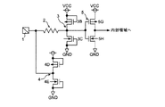
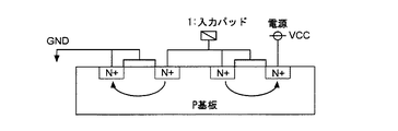
【解決手段】 この発明は、半導体集積回路のコア領域がCMOSで構成された半導体装置において、入力用回路セルの保護トランジスタ回路31(31B、31C)、41(41D、41E)が、Nチャネルトランジスタのみを用いて構成し、前記入力用回路セルを通った入力信号の初段のトランジスタ回路5は、内部コア領域に配置されている。
【選択図】 図4
Description
2 保護抵抗
31 保護トランジスタ回路
41 保護トランジスタ回路
5 コア領域の一部となるCMOS入力トランジスタ回路
Claims (1)
- 半導体集積回路のコア領域がCMOSで構成された半導体装置において、入力用回路セルが、NチャネルまたはPチャネルのどちらか一方のトランジスタのみを用いて構成されていることを特徴とする半導体装置。
Priority Applications (1)
| Application Number | Priority Date | Filing Date | Title |
|---|---|---|---|
| JP2005187403A JP2005294868A (ja) | 2005-06-27 | 2005-06-27 | 半導体装置 |
Applications Claiming Priority (1)
| Application Number | Priority Date | Filing Date | Title |
|---|---|---|---|
| JP2005187403A JP2005294868A (ja) | 2005-06-27 | 2005-06-27 | 半導体装置 |
Related Parent Applications (1)
| Application Number | Title | Priority Date | Filing Date |
|---|---|---|---|
| JP2001278339A Division JP2003086707A (ja) | 2001-09-13 | 2001-09-13 | 半導体装置 |
Publications (1)
| Publication Number | Publication Date |
|---|---|
| JP2005294868A true JP2005294868A (ja) | 2005-10-20 |
Family
ID=35327376
Family Applications (1)
| Application Number | Title | Priority Date | Filing Date |
|---|---|---|---|
| JP2005187403A Pending JP2005294868A (ja) | 2005-06-27 | 2005-06-27 | 半導体装置 |
Country Status (1)
| Country | Link |
|---|---|
| JP (1) | JP2005294868A (ja) |
Citations (10)
| Publication number | Priority date | Publication date | Assignee | Title |
|---|---|---|---|---|
| JPS59167036A (ja) * | 1983-03-14 | 1984-09-20 | Nec Corp | 半導体集積回路 |
| JPS6323349A (ja) * | 1986-07-16 | 1988-01-30 | Nec Corp | Cmos半導体集積回路 |
| JPH01235371A (ja) * | 1988-03-16 | 1989-09-20 | Nec Corp | 半導体集積回路装置 |
| JPH02146761A (ja) * | 1988-11-28 | 1990-06-05 | Nec Corp | 半導体集積回路装置 |
| JPH03205864A (ja) * | 1990-01-08 | 1991-09-09 | Hitachi Ltd | 電子回路 |
| JPH04196265A (ja) * | 1990-11-27 | 1992-07-16 | Mitsubishi Electric Corp | 半導体装置 |
| JPH10125801A (ja) * | 1996-09-06 | 1998-05-15 | Mitsubishi Electric Corp | 半導体集積回路装置 |
| JPH10340996A (ja) * | 1997-06-09 | 1998-12-22 | Nec Corp | 保護回路 |
| JPH11135717A (ja) * | 1997-10-27 | 1999-05-21 | Nec Corp | 半導体集積回路 |
| JP2001202772A (ja) * | 2000-01-20 | 2001-07-27 | Sanyo Electric Co Ltd | 半導体記憶装置 |
-
2005
- 2005-06-27 JP JP2005187403A patent/JP2005294868A/ja active Pending
Patent Citations (10)
| Publication number | Priority date | Publication date | Assignee | Title |
|---|---|---|---|---|
| JPS59167036A (ja) * | 1983-03-14 | 1984-09-20 | Nec Corp | 半導体集積回路 |
| JPS6323349A (ja) * | 1986-07-16 | 1988-01-30 | Nec Corp | Cmos半導体集積回路 |
| JPH01235371A (ja) * | 1988-03-16 | 1989-09-20 | Nec Corp | 半導体集積回路装置 |
| JPH02146761A (ja) * | 1988-11-28 | 1990-06-05 | Nec Corp | 半導体集積回路装置 |
| JPH03205864A (ja) * | 1990-01-08 | 1991-09-09 | Hitachi Ltd | 電子回路 |
| JPH04196265A (ja) * | 1990-11-27 | 1992-07-16 | Mitsubishi Electric Corp | 半導体装置 |
| JPH10125801A (ja) * | 1996-09-06 | 1998-05-15 | Mitsubishi Electric Corp | 半導体集積回路装置 |
| JPH10340996A (ja) * | 1997-06-09 | 1998-12-22 | Nec Corp | 保護回路 |
| JPH11135717A (ja) * | 1997-10-27 | 1999-05-21 | Nec Corp | 半導体集積回路 |
| JP2001202772A (ja) * | 2000-01-20 | 2001-07-27 | Sanyo Electric Co Ltd | 半導体記憶装置 |
Similar Documents
| Publication | Publication Date | Title |
|---|---|---|
| KR101231992B1 (ko) | 집적 회로 내의 esd 보호의 점유면적을 감소시키기 위한 방법 및 장치 | |
| JP4841204B2 (ja) | 半導体装置 | |
| US6222213B1 (en) | Semiconductor integrated circuit device | |
| JP3990352B2 (ja) | 半導体集積回路装置 | |
| CN103311239B (zh) | 跨域静电放电保护方案 | |
| US6756642B2 (en) | Integrated circuit having improved ESD protection | |
| JP2009130119A (ja) | 半導体集積回路 | |
| KR20110118671A (ko) | Esd 보호 디바이스가 집적된 신호 패드 및 파워 서플라이 | |
| US7420789B2 (en) | ESD protection system for multi-power domain circuitry | |
| KR20080076411A (ko) | 정전기 보호 회로 | |
| JPH11186497A (ja) | 半導体集積回路装置 | |
| US7649214B2 (en) | ESD protection system for multiple-domain integrated circuits | |
| CN101877583B (zh) | 缓冲装置及静电放电防护电路 | |
| US6218881B1 (en) | Semiconductor integrated circuit device | |
| KR100878439B1 (ko) | 출력 드라이버단의 esd 보호 장치 | |
| US7911751B2 (en) | Electrostatic discharge device with metal option ensuring a pin capacitance | |
| KR20180070470A (ko) | 반도체 칩 | |
| JP2005294868A (ja) | 半導体装置 | |
| US20070091523A1 (en) | ESD protection system for multi-power domain circuitry | |
| JP2004179470A (ja) | 半導体入出力回路 | |
| JP2003086707A (ja) | 半導体装置 | |
| US20080165459A1 (en) | Pad ESD Spreading Technique | |
| JP2001267496A (ja) | 入力保護回路を備えた半導体装置 | |
| JP2005347591A (ja) | スタンダードセル、スタンダードセル方式の半導体集積回路装置および半導体集積回路装置のレイアウト設計方法 | |
| JP5069872B2 (ja) | 半導体集積回路 |
Legal Events
| Date | Code | Title | Description |
|---|---|---|---|
| A621 | Written request for application examination |
Free format text: JAPANESE INTERMEDIATE CODE: A621 Effective date: 20070219 |
|
| RD02 | Notification of acceptance of power of attorney |
Free format text: JAPANESE INTERMEDIATE CODE: A7422 Effective date: 20090731 |
|
| RD05 | Notification of revocation of power of attorney |
Free format text: JAPANESE INTERMEDIATE CODE: A7425 Effective date: 20090909 |
|
| A131 | Notification of reasons for refusal |
Free format text: JAPANESE INTERMEDIATE CODE: A131 Effective date: 20110105 |
|
| A521 | Written amendment |
Free format text: JAPANESE INTERMEDIATE CODE: A523 Effective date: 20110304 |
|
| A02 | Decision of refusal |
Free format text: JAPANESE INTERMEDIATE CODE: A02 Effective date: 20110412 |