JP2005298910A - Copper alloy plate for conductive parts and manufacturing method thereof - Google Patents
Copper alloy plate for conductive parts and manufacturing method thereof Download PDFInfo
- Publication number
- JP2005298910A JP2005298910A JP2004117479A JP2004117479A JP2005298910A JP 2005298910 A JP2005298910 A JP 2005298910A JP 2004117479 A JP2004117479 A JP 2004117479A JP 2004117479 A JP2004117479 A JP 2004117479A JP 2005298910 A JP2005298910 A JP 2005298910A
- Authority
- JP
- Japan
- Prior art keywords
- copper alloy
- thickness
- conductive parts
- alloy plate
- heat treatment
- Prior art date
- Legal status (The legal status is an assumption and is not a legal conclusion. Google has not performed a legal analysis and makes no representation as to the accuracy of the status listed.)
- Granted
Links
- 229910000881 Cu alloy Inorganic materials 0.000 title claims abstract description 37
- 238000004519 manufacturing process Methods 0.000 title claims abstract description 7
- 238000010438 heat treatment Methods 0.000 claims abstract description 22
- 239000010949 copper Substances 0.000 claims abstract description 17
- 239000000956 alloy Substances 0.000 claims abstract description 13
- 238000005096 rolling process Methods 0.000 claims abstract description 13
- 229910052698 phosphorus Inorganic materials 0.000 claims abstract description 9
- 239000000203 mixture Substances 0.000 claims abstract description 8
- 229910052718 tin Inorganic materials 0.000 claims abstract description 7
- 239000012535 impurity Substances 0.000 claims abstract description 6
- 229910045601 alloy Inorganic materials 0.000 claims abstract description 4
- 238000005097 cold rolling Methods 0.000 claims description 17
- 238000007747 plating Methods 0.000 claims description 14
- 239000010410 layer Substances 0.000 claims description 11
- 229910052759 nickel Inorganic materials 0.000 claims description 4
- 239000011247 coating layer Substances 0.000 claims description 2
- 239000000463 material Substances 0.000 abstract description 29
- RYGMFSIKBFXOCR-UHFFFAOYSA-N Copper Chemical compound [Cu] RYGMFSIKBFXOCR-UHFFFAOYSA-N 0.000 abstract description 3
- 229910052802 copper Inorganic materials 0.000 abstract description 3
- 238000012545 processing Methods 0.000 abstract description 2
- 239000002131 composite material Substances 0.000 abstract 1
- 238000005452 bending Methods 0.000 description 12
- 238000005260 corrosion Methods 0.000 description 11
- 230000007797 corrosion Effects 0.000 description 11
- 239000013067 intermediate product Substances 0.000 description 6
- 229910001369 Brass Inorganic materials 0.000 description 4
- 229910000906 Bronze Inorganic materials 0.000 description 4
- OAICVXFJPJFONN-UHFFFAOYSA-N Phosphorus Chemical compound [P] OAICVXFJPJFONN-UHFFFAOYSA-N 0.000 description 4
- 238000000137 annealing Methods 0.000 description 4
- 239000010951 brass Substances 0.000 description 4
- 239000010974 bronze Substances 0.000 description 4
- 150000001875 compounds Chemical class 0.000 description 4
- KUNSUQLRTQLHQQ-UHFFFAOYSA-N copper tin Chemical compound [Cu].[Sn] KUNSUQLRTQLHQQ-UHFFFAOYSA-N 0.000 description 4
- 238000005336 cracking Methods 0.000 description 4
- 230000000694 effects Effects 0.000 description 4
- 238000000034 method Methods 0.000 description 3
- 238000012360 testing method Methods 0.000 description 3
- 229910018104 Ni-P Inorganic materials 0.000 description 2
- 229910018536 Ni—P Inorganic materials 0.000 description 2
- 238000005266 casting Methods 0.000 description 2
- 230000000052 comparative effect Effects 0.000 description 2
- 238000001816 cooling Methods 0.000 description 2
- 238000006073 displacement reaction Methods 0.000 description 2
- 239000011159 matrix material Substances 0.000 description 2
- 238000002844 melting Methods 0.000 description 2
- 230000008018 melting Effects 0.000 description 2
- 238000013508 migration Methods 0.000 description 2
- 230000005012 migration Effects 0.000 description 2
- 238000005554 pickling Methods 0.000 description 2
- 229920006395 saturated elastomer Polymers 0.000 description 2
- 239000002699 waste material Substances 0.000 description 2
- XLYOFNOQVPJJNP-UHFFFAOYSA-N water Substances O XLYOFNOQVPJJNP-UHFFFAOYSA-N 0.000 description 2
- 239000011248 coating agent Substances 0.000 description 1
- 238000000576 coating method Methods 0.000 description 1
- 238000004891 communication Methods 0.000 description 1
- 238000002788 crimping Methods 0.000 description 1
- 239000006185 dispersion Substances 0.000 description 1
- 238000004090 dissolution Methods 0.000 description 1
- 238000009429 electrical wiring Methods 0.000 description 1
- 238000011156 evaluation Methods 0.000 description 1
- 230000001747 exhibiting effect Effects 0.000 description 1
- 239000007789 gas Substances 0.000 description 1
- 238000005098 hot rolling Methods 0.000 description 1
- 230000006698 induction Effects 0.000 description 1
- 239000011261 inert gas Substances 0.000 description 1
- 238000003780 insertion Methods 0.000 description 1
- 230000037431 insertion Effects 0.000 description 1
- 238000011835 investigation Methods 0.000 description 1
- 239000002184 metal Substances 0.000 description 1
- 229910052751 metal Inorganic materials 0.000 description 1
- 235000021110 pickles Nutrition 0.000 description 1
- 239000002244 precipitate Substances 0.000 description 1
- 230000001376 precipitating effect Effects 0.000 description 1
- 238000001556 precipitation Methods 0.000 description 1
- 239000000047 product Substances 0.000 description 1
- 238000010791 quenching Methods 0.000 description 1
- 230000000171 quenching effect Effects 0.000 description 1
- 239000002994 raw material Substances 0.000 description 1
- 230000001105 regulatory effect Effects 0.000 description 1
- 229910000679 solder Inorganic materials 0.000 description 1
- 239000000126 substance Substances 0.000 description 1
- 238000004381 surface treatment Methods 0.000 description 1
- 230000037303 wrinkles Effects 0.000 description 1
Landscapes
- Conductive Materials (AREA)
Abstract
【課題】薄板導電部品に適した特性を具備する銅合金材料を提供する。
【解決手段】Ni:0.1〜3.0%,Sn:0.1〜2.0%,P:0.01〜0.3%、残部がCuおよび不可避的不純物からなり、好ましくはNi/Pが10〜30であり、0.2%耐力が600N/mm2以上、導電率が35%IACS以上、ヤング率が120kN/mm2以上、ばね限界値が400N/mm2以上であり、板厚が好ましくは0.15mm以下の薄板導電部品用銅合材料。この合金材料は、上記組成の合金板材に対し、300〜750℃に加熱後急冷する熱処理、10%以上の圧延率で板厚を0.15mm以下まで減じる冷間圧延、150〜600℃に加熱する熱処理、を順次施すことにより製造できる。
【選択図】なしA copper alloy material having characteristics suitable for thin plate conductive parts is provided.
Ni: 0.1-3.0%, Sn: 0.1-2.0%, P: 0.01-0.3%, the balance being Cu and inevitable impurities, preferably Ni / P is 10-30, 0.2% proof stress is 600 N / mm 2 or more, conductivity is 35% IACS or more, Young's modulus is 120 kN / mm 2 or more, spring limit value is 400 N / mm 2 or more, A copper composite material for thin plate conductive parts having a plate thickness of preferably 0.15 mm or less. This alloy material is a heat treatment in which the alloy plate material having the above composition is heated to 300 to 750 ° C. and then rapidly cooled, cold rolled to reduce the plate thickness to 0.15 mm or less at a rolling rate of 10% or more, and heated to 150 to 600 ° C. It can manufacture by performing the heat processing to perform sequentially.
[Selection figure] None
Description
本発明は、コネクタ,スイッチ,リレー等の電気・電子部品であって、特に板厚の薄い導電性部品に好適な銅合金材料およびその製造法に関する。 The present invention relates to a copper alloy material suitable for electrical / electronic parts such as connectors, switches, relays, etc., and particularly conductive parts having a thin plate thickness, and a method for manufacturing the same.
近年の情報通信機器、家電製品、自動車用部品等の電気配線は複雑化,高集積化が進んでいる。それに伴いコネクタ,スイッチ,リレー等の電気・電子部品用に使用される伸銅品材料の需要が増大している。 In recent years, electrical wiring of information communication devices, home appliances, automobile parts, etc. has become more complex and highly integrated. Along with this, the demand for copper products used for electrical and electronic parts such as connectors, switches and relays is increasing.
従来、コネクタ等の導電部品には黄銅やりん青銅が一般的に使用されてきた。
黄銅は低コスト材料として選択される。しかし、引張強さは質別がEHでも600N/mm2を超えず、薄板の電気接点材料としては強度面で必ずしも十分ではない。また、耐食性,耐応力腐食割れ性,耐応力緩和特性について多少劣る面があり、用途によっては使用に制約を受ける。
りん青銅は強度,耐食性,耐応力腐食割れ性,耐応力緩和特性のバランスに優れている。しかし、導電率が例えばばね用りん青銅で12%IACSと小さい。また、素材コストが高い。
Conventionally, brass and phosphor bronze have been generally used for conductive parts such as connectors.
Brass is selected as a low cost material. However, the tensile strength does not exceed 600 N / mm 2 even if the type is EH, and is not necessarily sufficient in terms of strength as a thin plate electrical contact material. In addition, the corrosion resistance, stress corrosion cracking resistance, and stress relaxation resistance are somewhat inferior, and use is restricted depending on the application.
Phosphor bronze has an excellent balance of strength, corrosion resistance, stress corrosion cracking resistance, and stress relaxation resistance. However, the conductivity is as small as 12% IACS, for example, for spring phosphor bronze. In addition, the material cost is high.
そこで、種々の銅合金が研究、開発され提案されている。なかでも下記特許文献1には、Ni−P系の析出物を均一分散させた端子用銅基合金が開示されている。これは、引張強さ,ばね限界値,導電率,耐応力緩和特性,曲げ加工性のすべてにおいて適度な高性能をバランスさせたものであり、コネクタ等の多くの導電用途に有用な材料である。 Therefore, various copper alloys have been researched, developed and proposed. In particular, the following Patent Document 1 discloses a copper-based alloy for terminals in which Ni—P-based precipitates are uniformly dispersed. This balances moderate high performance in all of tensile strength, spring limit value, electrical conductivity, stress relaxation resistance and bending workability, and is a useful material for many conductive applications such as connectors. .
昨今、電気・電子部品は小型化、軽量化される傾向にあり、それに使用される導電部品には必然的に薄肉化,細線化の要求が高まっている。この要求に応えるためには、薄肉化した場合でも優れた耐久性・高信頼性を発揮する材料が望まれる。具体的には、従来よりも一層高レベルの強度,導電性を呈することはもちろんのこと、高い耐力や弾性(ヤング率)を有することも重要となるのである。また、それらを改善する際、耐食性や複雑形状へのプレス成形性を劣化させてはならない。加えて、材料コストの増大も避けなければならない。 In recent years, electric and electronic parts tend to be reduced in size and weight, and conductive parts used for such parts are inevitably required to be thinner and thinner. In order to meet this demand, a material that exhibits excellent durability and high reliability even when it is thinned is desired. Specifically, it is important to have a higher strength and elasticity (Young's modulus) as well as exhibiting a higher level of strength and conductivity than before. Moreover, when improving them, corrosion resistance and press formability to a complicated shape must not be deteriorated. In addition, an increase in material costs must be avoided.
特許文献1に開示の銅合金材料は前述のように、強度や導電性の良好なバランスを有しており、従来主流であった板厚が0.2mm前後の導電部品として使用するには特に問題はなかった。しかしながら、昨今では板厚0.15mm以下、あるいはそれ未満のニーズが増加している。具体的には0.10mm,0.08mm,0.05mmといった薄板導電部品の要求が強くなっている。特許文献1の銅合金材料は、これらの極薄部品に使用するには強度レベルが不足する場合があり、ヤング率も115kN/mm2前後であり十分とは言えない。すなわち、極薄導電部品用としては信頼性に欠ける面があった。 As described above, the copper alloy material disclosed in Patent Document 1 has a good balance of strength and conductivity, and is particularly suitable for use as a conductive component having a plate thickness of about 0.2 mm, which has been the mainstream in the past. There was no problem. However, in recent years, the need for a plate thickness of 0.15 mm or less or less has increased. Specifically, there is an increasing demand for thin plate conductive parts such as 0.10 mm, 0.08 mm, and 0.05 mm. The copper alloy material of Patent Document 1 may be insufficient in strength level for use in these ultra-thin parts, and the Young's modulus is about 115 kN / mm 2, which is not sufficient. That is, there was a lack of reliability for ultrathin conductive parts.
本発明は、上記のような導電部品の薄肉化に十分対応できる優れた機械的特性を有し、かつ導電部品に要求される耐食性,導電性等の基本的特性も具備した銅合金材料をコスト増を抑えながら安定して供給しようというものである。 The present invention provides a copper alloy material that has excellent mechanical characteristics that can sufficiently cope with the thinning of conductive parts as described above, and that also has basic characteristics such as corrosion resistance and conductivity required for conductive parts. It is intended to supply stably while suppressing the increase.
発明者らの検討の結果、上記目的は特許文献1に開示の組成を有する銅合金をベースとして実現可能であることが明らかになった。すなわち、本発明で提供する材料は、Ni:0.1〜3.0%,Sn:0.1〜2.0%,P:0.01〜0.3%、残部がCuおよび不可避的不純物からなり、好ましくは下記(1)式を満たし、0.2%耐力が600N/mm2以上、導電率が35%IACS以上、ヤング率が120kN/mm2以上、ばね限界値が400N/mm2以上の銅合金であり、好ましくは板厚が0.15mm以下の薄板導電部品用銅合金板である。
10≦Ni/P≦30 ……(1)
ここで、(1)式のNi,Pの箇所には質量%で表されたこれらの元素の含有量が代入される。「銅合金板」には帯板が含まれる。
As a result of investigations by the inventors, it has been clarified that the above object can be realized based on a copper alloy having the composition disclosed in Patent Document 1. That is, the materials provided by the present invention are Ni: 0.1-3.0%, Sn: 0.1-2.0%, P: 0.01-0.3%, the balance being Cu and inevitable impurities consists, preferably satisfies the following equation (1), 0.2% proof stress 600N / mm 2 or more, conductivity of 35% IACS or more, a Young's modulus of 120 kN / mm 2 or more, the spring limit value 400 N / mm 2 The above copper alloy, preferably a copper alloy plate for a thin plate conductive part having a plate thickness of 0.15 mm or less.
10 ≦ Ni / P ≦ 30 (1)
Here, the contents of these elements expressed in mass% are substituted for Ni and P in the formula (1). The “copper alloy plate” includes a strip.
この合金材料には導電性の被覆層を形成することができる。特に、厚さ0.3〜2.0μmのCuめっき層およびその上に厚さ0.5〜5.0μmのSnめっき層を有する材料が提供される。 A conductive coating layer can be formed on the alloy material. In particular, a material having a Cu plating layer having a thickness of 0.3 to 2.0 μm and a Sn plating layer having a thickness of 0.5 to 5.0 μm thereon is provided.
また、その導電部品用銅合金板は、前記所定の組成を有する銅合金材料に対し、
300〜750℃に加熱後急冷する熱処理、
10%以上の圧延率で板厚を0.15mm以下まで減じる冷間圧延、
150〜600℃に加熱する熱処理、
を順次施す方法により製造することができる。
Further, the copper alloy plate for conductive parts is a copper alloy material having the predetermined composition,
Heat treatment to be rapidly cooled after heating to 300-750 ° C.,
Cold rolling to reduce the sheet thickness to 0.15 mm or less at a rolling rate of 10% or more,
Heat treatment to heat to 150-600 ° C.,
Can be manufactured by a method of sequentially applying the above.
表面に厚さ0.3〜2.0μmのCuめっき層およびその上に厚さ0.5〜5.0μmのSnめっき層を形成した場合は、その後、100〜200℃に加熱する熱処理を施す製造法が採用される。 When a Cu plating layer having a thickness of 0.3 to 2.0 μm and a Sn plating layer having a thickness of 0.5 to 5.0 μm are formed on the surface, a heat treatment is performed by heating to 100 to 200 ° C. Manufacturing method is adopted.
本発明によれば、従来の材料では、機械的特性,導電性,耐食性を高レベルでバランスさせることが困難であったために実現できなかった、板厚0.15mm以下あるいはそれ未満の薄板導電部品に適した銅合金材料を安定的に提供することが可能になった。したがって本発明は、電気・電子部品の小型化・軽量化に寄与するものである。 According to the present invention, with conventional materials, it was difficult to balance mechanical properties, electrical conductivity, and corrosion resistance at a high level, and thus a thin plate conductive component having a thickness of 0.15 mm or less or less could not be realized. It became possible to stably provide a copper alloy material suitable for the above. Therefore, the present invention contributes to reducing the size and weight of electrical / electronic components.
〔化学組成〕
Niは、Cuマトリックス中に固溶して、母材の強度,弾性,耐熱性,耐応力緩和特性,耐マイグレーション性の向上に寄与する元素である。さらに、Pとの化合物を形成して分散析出させることにより電気伝導性の向上にも寄与する。これらの効果を十分に発揮させるためには、0.1質量%以上のNi含有が必要である。ただし、3.0質量%を超えると前記効果は飽和し、不経済となる。したがって、Ni含有量は0.1〜3.0質量%に規定する。
[Chemical composition]
Ni is an element that dissolves in the Cu matrix and contributes to improvement in strength, elasticity, heat resistance, stress relaxation resistance, and migration resistance of the base material. Furthermore, it contributes to the improvement of electrical conductivity by forming a compound with P to be dispersed and precipitated. In order to fully exhibit these effects, Ni content of 0.1% by mass or more is necessary. However, if it exceeds 3.0% by mass, the effect is saturated and uneconomical. Therefore, the Ni content is specified to be 0.1 to 3.0% by mass.
Snは、母材のマトリックス中に固溶して強度,弾性および耐食性を向上させる元素である。Sn含有量が0.1質量%未満では特に強度,弾性の向上が十分に達成できない。一方、2.0質量%を超えると前記効果は飽和し、不経済となる。したがって、Sn含有量は0.1〜2.0質量%に規定する。 Sn is an element that improves the strength, elasticity and corrosion resistance by dissolving in the matrix of the base material. When the Sn content is less than 0.1% by mass, the strength and elasticity cannot be improved sufficiently. On the other hand, if it exceeds 2.0% by mass, the effect becomes saturated and uneconomical. Therefore, Sn content is prescribed | regulated to 0.1-2.0 mass%.
Pは、溶湯の脱酸剤として作用するとともに、Niとの化合物を分散析出させることにより、電気伝導性を向上させ、且つ引張強さ,弾性,耐応力緩和特性を向上させる。P含有量が0.01質量%未満ではこれらの効果は十分に得られない。しかし、0.3質量%を超えるとNi共存下でも電気伝導性,加工性,はんだ耐候性の低下が顕著となり、さらに耐マイグレーション性の低下を招く。したがって、P含有量は0.01〜0.3質量%に規定する。 P acts as a deoxidizer for the molten metal, and improves the electrical conductivity and the tensile strength, elasticity, and stress relaxation resistance properties by dispersing and precipitating a compound with Ni. If the P content is less than 0.01% by mass, these effects cannot be obtained sufficiently. However, if it exceeds 0.3% by mass, the electrical conductivity, workability and solder weather resistance will be significantly reduced even in the presence of Ni, and further the migration resistance will be reduced. Therefore, the P content is defined as 0.01 to 0.3% by mass.
残部は実質的にCuからなる。
なお、本発明では前述のようにNiとPの化合物(Ni−P系化合物)の分散析出を利用して強度や導電性を向上させることから、Ni/Pの含有量(質量%)の比は10〜30の範囲とすることが望ましい。
The remainder consists essentially of Cu.
In the present invention, as described above, since the strength and conductivity are improved by utilizing the dispersion precipitation of the compound of Ni and P (Ni-P compound), the ratio of Ni / P content (% by mass). Is preferably in the range of 10-30.
〔材料特性〕
導電部品としての重要な用途であるコネクタにおいては、挿入時の応力負荷や曲げに対して座屈や変形が生じない強度が必要であり、さらに電線の加締め,保持に対する強度も必要である。板厚0.15mm以下あるいはそれ未満の薄板材料を想定した場合、0.2%耐力は600N/mm2以上が必要であり、できれば650N/mm2以上が望まれる。ばね限界値は400N/mm2以上が必要であり、できれば500N/mm2以上、さらに好ましくは520N/mm2以上が望まれる。引張強さについては630N/mm2以上を確保することが望ましい。
〔Material property〕
A connector, which is an important application as a conductive component, needs to be strong enough not to buckle or deform against stress load or bending at the time of insertion, and also needs to have strength against crimping and holding of an electric wire. Assuming a thin plate material having a thickness of 0.15 mm or less or less, the 0.2% proof stress should be 600 N / mm 2 or more, and preferably 650 N / mm 2 or more. The spring limit value is required to be 400 N / mm 2 or more, preferably 500 N / mm 2 or more, more preferably 520 N / mm 2 or more. Tensile strength it is desirable to ensure a 630 N / mm 2 or more.
また、最近はコネクタ自体が小型化され、ヤング率の大きな材料でばねの変位を小さくとる構造が有利になっている。つまり、小さな変位で大きな応力が得られる高ヤング率の材料が望まれている。特に板厚0.15mm以下あるいはそれ未満の薄板材料を使用する場合は、ヤング率が120kN/mm2以上であることが要求され、できれば130kN/mm2以上が一層好ましい。
コネクタの小型化によりプレス成形性の要求も厳しくなり、曲げ部半径(R)と板厚(t)の比R/tが1以下を満足するような加工性が望まれる。
Recently, the connector itself has been downsized, and a structure in which the spring displacement is made small with a material having a large Young's modulus is advantageous. That is, a material having a high Young's modulus capable of obtaining a large stress with a small displacement is desired. In particular, when a thin plate material having a thickness of 0.15 mm or less or less is used, the Young's modulus is required to be 120 kN / mm 2 or more, and more preferably 130 kN / mm 2 or more.
Due to the downsizing of the connector, the demand for press formability becomes strict, and the workability that satisfies the ratio R / t of the bending portion radius (R) to the plate thickness (t) of 1 or less is desired.
導電性については、特に板厚0.15mm以下あるいはそれ未満の導電部品における通電時のジュール熱発生を十分抑えるために、35%IACS以上の導電率が必要であり、できれば40%IACS以上が望まれるところである。 Regarding conductivity, in order to sufficiently suppress the generation of Joule heat at the time of energization especially in a conductive part having a thickness of 0.15 mm or less, a conductivity of 35% IACS or more is necessary, and preferably 40% IACS or more is desirable. It is where
さらに、耐食性,耐応力腐食割れ性に優れていることが望まれ、またメス端子に至っては熱的負荷が加わることから耐応力緩和特性に優れることも重要となる。具体的には、応力腐食割れ寿命は従来の黄銅1種の3倍以上、応力緩和率は150℃×500時間の緩和率が黄銅1種の半分である25%以下であることが望ましい。 Furthermore, it is desired to have excellent corrosion resistance and stress corrosion cracking resistance, and since a thermal load is applied to the female terminal, it is also important to have excellent stress relaxation characteristics. Specifically, it is desirable that the stress corrosion cracking life is 3 times or more of one type of conventional brass, and the stress relaxation rate is 25% or less where the relaxation rate of 150 ° C. × 500 hours is half that of one type of brass.
〔表面処理〕
以上の銅合金板には導電性の表面被覆を施すことができる。例えば、表面に厚さ0.3〜2.0μmのCuめっき層およびその上に厚さ0.5〜5.0μmのSnめっき層を有するものは、コネクタ等において一層高い耐久性を呈する。
〔surface treatment〕
The above copper alloy plate can be provided with a conductive surface coating. For example, a Cu plating layer having a thickness of 0.3 to 2.0 μm on the surface and a Sn plating layer having a thickness of 0.5 to 5.0 μm thereon have higher durability in a connector or the like.
〔製造法〕
前記のような特性を有する導電部品用銅合金板は、以下のようにして製造することができる。
まず、前述の組成を有する銅合金を溶製し、通常の手法で熱間圧延し、冷間圧延と焼鈍を繰り返して中間製品(焼鈍材)を作る。この中間製品の板厚は、その後に行う最終的な冷間圧延(以下、これを「仕上冷間圧延」という)において、0.15mmあるいはそれ未満の目標板厚まで中間焼鈍なしで冷間圧延が可能となる板厚とする必要がある。ただし、仕上冷間圧延で少なくとも10%以上の圧延率が確保できるように、中間製品の板厚を設定する。
[Production method]
The copper alloy plate for conductive parts having the above-described characteristics can be manufactured as follows.
First, a copper alloy having the above composition is melted and hot-rolled by a normal method, and cold rolling and annealing are repeated to produce an intermediate product (annealed material). The sheet thickness of this intermediate product is cold rolled without intermediate annealing to the final sheet thickness of 0.15 mm or less in the final cold rolling (hereinafter referred to as “finished cold rolling”) performed thereafter. It is necessary to make the plate thickness that enables this. However, the plate thickness of the intermediate product is set so that a rolling rate of at least 10% or more can be secured by finish cold rolling.
中間製品を作る際の最後の熱処理では、材料を300〜750℃に加熱したのち、水冷等により急冷することが重要である。上記温度範囲での保持時間は1〜360分とすることができるが、通常、30〜120分程度とすることが望ましい。加熱温度範囲は450〜650℃とすることが好ましく、500〜600℃が一層好ましい。冷却後は酸洗等により表面の酸化スケールを除去しておく。 In the final heat treatment for producing the intermediate product, it is important that the material is heated to 300 to 750 ° C. and then rapidly cooled by water cooling or the like. Although the holding time in the said temperature range can be 1-360 minutes, it is desirable to set it as about 30-120 minutes normally. The heating temperature range is preferably 450 to 650 ° C, more preferably 500 to 600 ° C. After cooling, the surface oxide scale is removed by pickling or the like.
次に仕上冷間圧延を施す。ここでは板厚を0.15mm以下あるいはそれ未満に減少させること、および少なくとも10%以上の圧延率を確保することが必要である。できれば50%以上の圧延率を確保することが望ましい。板厚をこのような薄い領域まで減少させるには、へリングボーンの発生防止に注力する必要がある。また、特に0.10mm,0.05mmといった極薄材の場合、板厚精度の確保にも注意が必要である。このような薄板の圧延は、板に通常の冷間圧延の2倍前後の張力を加えることで可能となる。具体的には仕上冷間圧延直後の材料の0.2%耐力に対し、その30%以上の張力を加えることが望ましい。 Next, finish cold rolling is performed. Here, it is necessary to reduce the plate thickness to 0.15 mm or less and to ensure a rolling rate of at least 10%. If possible, it is desirable to secure a rolling rate of 50% or more. In order to reduce the plate thickness to such a thin region, it is necessary to focus on preventing the generation of herringbone. In particular, in the case of an extremely thin material such as 0.10 mm and 0.05 mm, attention must be paid to securing the plate thickness accuracy. Such a thin plate can be rolled by applying a tension of about twice the normal cold rolling to the plate. Specifically, it is desirable to apply a tension of 30% or more to the 0.2% yield strength of the material immediately after finish cold rolling.
次いで、材料を150〜600℃に加熱する熱処理を施す。上記温度範囲での保持時間は5秒〜180分の広範囲で実施できるが、通常、10〜60分程度とすることが望ましい。加熱温度範囲は200〜350℃とすることが一層好ましい。この熱処理後も酸洗することが望ましい。
このようにして、前記の優れた特性を有する銅合金板を得ることができる。
Subsequently, the heat processing which heats material to 150-600 degreeC is performed. Although the holding time in the above temperature range can be carried out over a wide range of 5 seconds to 180 minutes, it is usually desirable to be about 10 to 60 minutes. The heating temperature range is more preferably 200 to 350 ° C. It is desirable to pickle even after this heat treatment.
In this way, a copper alloy plate having the above-described excellent characteristics can be obtained.
この銅合金板の表面に前述した厚さ0.3〜2.0μmのCuめっき層およびその上に厚さ0.5〜5.0μmのSnめっき層を施す場合は、めっき後に100〜200℃の温度範囲で材料を加熱することが望ましい。この熱処理により、ばね限界値が向上し、また、曲げ加工部での硬化が大きくなるのでコネクタ材料として一層有利となる。 When the Cu plating layer having a thickness of 0.3 to 2.0 μm and the Sn plating layer having a thickness of 0.5 to 5.0 μm are applied on the surface of the copper alloy plate, the temperature is 100 to 200 ° C. after plating. It is desirable to heat the material in the temperature range. By this heat treatment, the spring limit value is improved and the hardening at the bent portion is increased, which is further advantageous as a connector material.
なお、合金の原料としてSnめっき層を有する材料のプレス打ち抜き屑を使用する場合は、予め溶解前に当該屑を大気中または不活性ガス雰囲気中で300〜600℃,0.5〜24時間保持する熱処理に供しておくことが望ましい。 In addition, when using the stamping waste of the material which has Sn plating layer as a raw material of an alloy, the said waste is previously hold | maintained at 300-600 degreeC and 0.5 to 24 hours in air | atmosphere or inert gas atmosphere before melt | dissolution. It is desirable to be subjected to heat treatment.
Ni,Sn,Pの含有量を調整した銅合金を高周波誘導溶解炉を用いて溶製し、40mm×40mm×150mmの鋳塊を得た。その際、溶解から鋳造までの雰囲気はArガス雰囲気とし、鋳造後直ちに水冷した。
各鋳塊を熱間圧延したのち、冷間圧延と焼鈍を繰り返して板厚0.5〜1.4mmの中間製品(焼鈍材)を得た。中間製品を作る際の最後の熱処理は、550℃×60分保持後、水急冷する方法で行った。
A copper alloy in which the contents of Ni, Sn, and P were adjusted was melted using a high frequency induction melting furnace to obtain a 40 mm × 40 mm × 150 mm ingot. At that time, the atmosphere from melting to casting was an Ar gas atmosphere, and water-cooled immediately after casting.
After each ingot was hot-rolled, cold rolling and annealing were repeated to obtain an intermediate product (annealed material) having a plate thickness of 0.5 to 1.4 mm. The final heat treatment for producing the intermediate product was performed by water quenching after holding at 550 ° C. for 60 minutes.
その後、酸洗し、10%以上の圧延率で最終的に板厚0.08mm,0.10,あるいは0.25mmまで冷間圧延した(仕上冷間圧延)。なお、この仕上冷間圧延時には、張力を各材料の仕上冷間圧延直後の0.2%耐力に対し19%,27%,37%,44%の各水準で付与しながら最終板厚まで冷間圧延を試み、ヘリングボーンの発生状況を調べた。 Thereafter, pickling was performed, and cold rolling was finally performed at a rolling rate of 10% or more to a plate thickness of 0.08 mm, 0.10, or 0.25 mm (finish cold rolling). At the time of finish cold rolling, the tension is applied to the final sheet thickness while applying tensions of 19%, 27%, 37% and 44% to the 0.2% proof stress immediately after the finish cold rolling of each material. We tried hot rolling to investigate the occurrence of herringbone.
次いで、前記仕上圧延で張力を0.2%耐力の44%付与して圧延した材料について、150〜350℃×30分保持の熱処理を行った。この熱処理をここでは「低温焼鈍」と称する。その後、酸洗した。 Next, heat treatment was performed on the material that was rolled by the finish rolling with 44% of 0.2% proof stress and held at 150 to 350 ° C. for 30 minutes. This heat treatment is referred to herein as “low temperature annealing”. Then, it pickled.
以上のようにして得られた銅合金板を試験材として、導電率,ビッカース硬さ,引張特性(引張強さσB,0.2%耐力σ0.2),ばね限界値,曲げ加工性,ヤング率を求めた。
導電率はJIS H 0505、ビッカース硬さはJIS Z 2244、引張特性はJIS Z 2241、ばね限界値はJIS H 3130の繰り返したわみ式試験、ヤング率はJIS Z 2280にそれぞれ準じて求めた。
曲げ加工性は、90°W曲げ試験(CES−M−0002−6,R=0.1mm,R/t=1.25,W=10mm,圧延方向)を行い、中央部の山表面が良好なものを○評価、シワが発生したものを△評価、割れの発生したものを×評価とした。
Using the copper alloy sheet obtained as described above as a test material, conductivity, Vickers hardness, tensile properties (tensile strength σ B , 0.2% proof stress σ 0.2 ), spring limit value, bending workability, Young The rate was determined.
The electrical conductivity was determined in accordance with JIS Z 2244, the Vickers hardness was determined in accordance with JIS Z 2244, the tensile property was determined in accordance with JIS Z 2241, the spring limit was determined in accordance with JIS H 3130, and the Young's modulus was determined in accordance with JIS Z 2280.
The bending workability is 90 ° W bending test (CES-M-0002-6, R = 0.1 mm, R / t = 1.25, W = 10 mm, rolling direction), and the central mountain surface is good. An evaluation was given as “◯”, a case where wrinkles occurred was evaluated as “Δ”, and a case where cracks occurred was evaluated as “X”.
結果を表1に示す。
なお、引張強さσB,0.2%耐力σ0.2,ばね限界値,ヤング率の試験片はいずれも長手方向が圧延方向と直角方向(TD)になるようにした。
表1の曲げ加工性において、「G.W.(R=0)」は曲げ軸が圧延方向に垂直、曲げ半径Rが0の場合を意味し、「B.W.(R=0.1)」は曲げ軸が圧延方向に平行、曲げ半径Rが0.1mmの場合を意味する。
The results are shown in Table 1.
The tensile strength σ B , 0.2% proof stress σ 0.2 , spring limit value, Young's modulus test pieces were all set so that the longitudinal direction was perpendicular to the rolling direction (TD).
In the bending workability in Table 1, “GW (R = 0)” means that the bending axis is perpendicular to the rolling direction and the bending radius R is 0, and “BW (R = 0.1)” means that the bending axis is the rolling direction. , And the bending radius R is 0.1 mm.
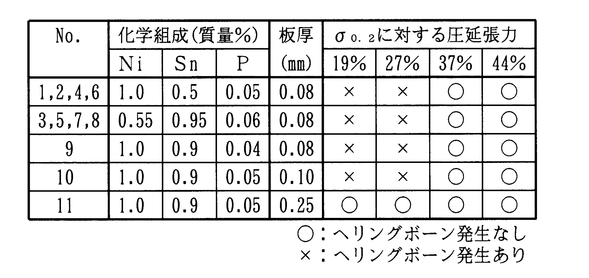
表1からわかるように、本発明例であるNo.1〜10は、板厚が0.08〜0.10mmと薄いにもかかわらず、0.2%耐力は600N/mm2以上を十分クリアし、また、ヤング率も120kN/mm2を余裕をもって上回った。比較例のC5210は従来のりん青銅であるが、これと比べると優れた導電率を呈し、曲げ加工性,ヤング率も勝った。
比較例No.11は仕上冷間圧延で板厚を0.25mmまでしか減じなかったため、0.2%耐力が600N/mm2に達しなかった。
As can be seen from Table 1, Nos. 1 to 10, which are examples of the present invention, sufficiently clear 0.2% proof stress of 600 N / mm 2 or more despite the thin plate thickness of 0.08 to 0.10 mm. In addition, the Young's modulus exceeded 120 kN / mm 2 with a margin. C5210 of the comparative example is a conventional phosphor bronze, but has an excellent electrical conductivity, and also has excellent bending workability and Young's modulus.
In Comparative Example No. 11, the sheet thickness was only reduced to 0.25 mm by finish cold rolling, so the 0.2% proof stress did not reach 600 N / mm 2 .
表2に、仕上冷間圧延時のヘリングボーン発生に及ぼす張力の影響を示す。 Table 2 shows the influence of tension on the herringbone generation during finish cold rolling.
表2からわかるように、0.25mm程度の板厚までなら、特に高い張力を付与することなく容易にへリングボーンのない良好な表面を得ることができる。これに対し、目標板厚が0.08〜0.10mmの極薄レベルになると、張力を高めなければヘリングボーンの発生を防止することは困難である。 As can be seen from Table 2, when the plate thickness is about 0.25 mm, a good surface without a herringbone can be easily obtained without applying particularly high tension. On the other hand, when the target plate thickness is an extremely thin level of 0.08 to 0.10 mm, it is difficult to prevent the generation of herringbone unless the tension is increased.
Claims (7)
10≦Ni/P≦30 ……(1) Ni: 0.1 to 3.0%, Sn: 0.1 to 2.0%, P: 0.01 to 0.3%, the balance being Cu and inevitable impurities, and the following ( 1) it has a composition satisfying the formula, 0.2% proof stress 600N / mm 2 or more, conductivity of 35% IACS or more, a Young's modulus of 120 kN / mm 2 or more, the spring limit value is 400 N / mm 2 or more Copper alloy.
10 ≦ Ni / P ≦ 30 (1)
300〜750℃に加熱後急冷する熱処理、
10%以上の圧延率で板厚を0.15mm以下まで減じる冷間圧延、
150〜600℃に加熱する熱処理、
を順次施す、0.2%耐力が600N/mm2以上、導電率が35%IACS以上、ヤング率が120kN/mm2以上、ばね限界値が400N/mm2以上である導電部品用銅合金板の製造法。
10≦Ni/P≦30 ……(1) Ni: 0.1 to 3.0%, Sn: 0.1 to 2.0%, P: 0.01 to 0.3%, the balance being Cu and inevitable impurities, and the following ( For copper alloy sheets with a composition that satisfies the formula (1)
Heat treatment to be rapidly cooled after heating to 300-750 ° C.,
Cold rolling to reduce the sheet thickness to 0.15 mm or less at a rolling rate of 10% or more,
Heat treatment to heat to 150-600 ° C.,
The copper alloy plate for conductive parts having a 0.2% proof stress of 600 N / mm 2 or more, a conductivity of 35% IACS or more, a Young's modulus of 120 kN / mm 2 or more, and a spring limit value of 400 N / mm 2 or more. Manufacturing method.
10 ≦ Ni / P ≦ 30 (1)
300〜750℃に加熱後急冷する熱処理、
10%以上の圧延率で板厚を0.15mm以下まで減じる冷間圧延、
150〜600℃に加熱する熱処理、
を順次施して得られた0.2%耐力が600N/mm2以上、導電率が35%IACS以上、ヤング率が120kN/mm2以上、ばね限界値が400N/mm2以上である銅合金板の表面に、厚さ0.3〜2.0μmのCuめっきを施し、さらにその上に厚さ0.5〜5.0μmのSnめっきを施し、その後、100〜200℃に加熱する熱処理を施す、導電部品用銅合金板の製造法。
10≦Ni/P≦30 ……(1) Ni: 0.1 to 3.0%, Sn: 0.1 to 2.0%, P: 0.01 to 0.3%, the balance being Cu and inevitable impurities, and the following ( For copper alloy sheets with a composition that satisfies the formula (1)
Heat treatment to be rapidly cooled after heating to 300-750 ° C.,
Cold rolling to reduce the sheet thickness to 0.15 mm or less at a rolling rate of 10% or more,
Heat treatment to heat to 150-600 ° C.,
Alloy sheet obtained by sequentially applying 0.2% proof stress, having a 0.2% proof stress of 600 N / mm 2 or more, a conductivity of 35% IACS or more, a Young's modulus of 120 kN / mm 2 or more, and a spring limit value of 400 N / mm 2 or more. A Cu plating with a thickness of 0.3 to 2.0 μm is applied to the surface of the film, and a Sn plating with a thickness of 0.5 to 5.0 μm is further applied thereon, followed by a heat treatment to be heated to 100 to 200 ° C. The manufacturing method of the copper alloy plate for conductive parts.
10 ≦ Ni / P ≦ 30 (1)
Priority Applications (1)
| Application Number | Priority Date | Filing Date | Title |
|---|---|---|---|
| JP2004117479A JP4633380B2 (en) | 2004-04-13 | 2004-04-13 | Manufacturing method of copper alloy sheet for conductive parts |
Applications Claiming Priority (1)
| Application Number | Priority Date | Filing Date | Title |
|---|---|---|---|
| JP2004117479A JP4633380B2 (en) | 2004-04-13 | 2004-04-13 | Manufacturing method of copper alloy sheet for conductive parts |
Publications (2)
| Publication Number | Publication Date |
|---|---|
| JP2005298910A true JP2005298910A (en) | 2005-10-27 |
| JP4633380B2 JP4633380B2 (en) | 2011-02-16 |
Family
ID=35330820
Family Applications (1)
| Application Number | Title | Priority Date | Filing Date |
|---|---|---|---|
| JP2004117479A Expired - Lifetime JP4633380B2 (en) | 2004-04-13 | 2004-04-13 | Manufacturing method of copper alloy sheet for conductive parts |
Country Status (1)
| Country | Link |
|---|---|
| JP (1) | JP4633380B2 (en) |
Cited By (5)
| Publication number | Priority date | Publication date | Assignee | Title |
|---|---|---|---|---|
| JP2006083420A (en) * | 2004-09-15 | 2006-03-30 | Dowa Mining Co Ltd | Copper alloy with improved conductivity and method for producing the same |
| KR100749334B1 (en) | 2006-04-14 | 2007-08-14 | 김창락 | Rolled heat treatment method of copper alloy sheet and its apparatus |
| JP2007270300A (en) * | 2006-03-31 | 2007-10-18 | Dowa Holdings Co Ltd | Cu-Ni-Sn-P-based copper alloy and method for producing the same |
| CN110306077A (en) * | 2019-07-24 | 2019-10-08 | 宁波兴业盛泰集团有限公司 | A kind of electric connector Vulcan metal and preparation method thereof |
| CN111519064A (en) * | 2020-06-05 | 2020-08-11 | 浙江天河铜业股份有限公司 | A kind of manufacturing method of ultra-thin electronic grade copper strip based on the field of metal processing |
Citations (5)
| Publication number | Priority date | Publication date | Assignee | Title |
|---|---|---|---|---|
| JPH036341A (en) * | 1989-06-02 | 1991-01-11 | Dowa Mining Co Ltd | High strength and high conductivity copper-base alloy |
| JPH04154942A (en) * | 1990-10-17 | 1992-05-27 | Dowa Mining Co Ltd | Manufacture of copper base alloy for connector |
| JP2000256814A (en) * | 1999-03-03 | 2000-09-19 | Sumitomo Metal Mining Co Ltd | Manufacturing method of copper base alloy strip for terminal |
| JP2001262255A (en) * | 2000-03-17 | 2001-09-26 | Sumitomo Metal Mining Co Ltd | Copper base alloy strip for terminal and manufacturing method thereof |
| JP2001303159A (en) * | 2000-04-27 | 2001-10-31 | Dowa Mining Co Ltd | Copper alloy for connector and its manufacturing method |
-
2004
- 2004-04-13 JP JP2004117479A patent/JP4633380B2/en not_active Expired - Lifetime
Patent Citations (5)
| Publication number | Priority date | Publication date | Assignee | Title |
|---|---|---|---|---|
| JPH036341A (en) * | 1989-06-02 | 1991-01-11 | Dowa Mining Co Ltd | High strength and high conductivity copper-base alloy |
| JPH04154942A (en) * | 1990-10-17 | 1992-05-27 | Dowa Mining Co Ltd | Manufacture of copper base alloy for connector |
| JP2000256814A (en) * | 1999-03-03 | 2000-09-19 | Sumitomo Metal Mining Co Ltd | Manufacturing method of copper base alloy strip for terminal |
| JP2001262255A (en) * | 2000-03-17 | 2001-09-26 | Sumitomo Metal Mining Co Ltd | Copper base alloy strip for terminal and manufacturing method thereof |
| JP2001303159A (en) * | 2000-04-27 | 2001-10-31 | Dowa Mining Co Ltd | Copper alloy for connector and its manufacturing method |
Cited By (7)
| Publication number | Priority date | Publication date | Assignee | Title |
|---|---|---|---|---|
| JP2006083420A (en) * | 2004-09-15 | 2006-03-30 | Dowa Mining Co Ltd | Copper alloy with improved conductivity and method for producing the same |
| JP2007270300A (en) * | 2006-03-31 | 2007-10-18 | Dowa Holdings Co Ltd | Cu-Ni-Sn-P-based copper alloy and method for producing the same |
| KR100749334B1 (en) | 2006-04-14 | 2007-08-14 | 김창락 | Rolled heat treatment method of copper alloy sheet and its apparatus |
| CN110306077A (en) * | 2019-07-24 | 2019-10-08 | 宁波兴业盛泰集团有限公司 | A kind of electric connector Vulcan metal and preparation method thereof |
| CN110306077B (en) * | 2019-07-24 | 2021-12-03 | 宁波兴业盛泰集团有限公司 | Corrosion-resistant copper alloy for electric connector and preparation method thereof |
| CN111519064A (en) * | 2020-06-05 | 2020-08-11 | 浙江天河铜业股份有限公司 | A kind of manufacturing method of ultra-thin electronic grade copper strip based on the field of metal processing |
| CN111519064B (en) * | 2020-06-05 | 2021-04-16 | 浙江天河铜业股份有限公司 | Manufacturing method of ultrathin electronic-grade copper plate strip based on metal processing field |
Also Published As
| Publication number | Publication date |
|---|---|
| JP4633380B2 (en) | 2011-02-16 |
Similar Documents
| Publication | Publication Date | Title |
|---|---|---|
| JP4584692B2 (en) | High-strength copper alloy sheet excellent in bending workability and manufacturing method thereof | |
| US5334346A (en) | Copper alloys for electrical and electronic parts | |
| CN101792872B (en) | Containing the copper alloy of cobalt, nickel and silicon | |
| CN101012519A (en) | Silver containing copper alloy | |
| JP2006009137A (en) | Copper alloy | |
| JP4393663B2 (en) | Copper-based alloy strip for terminal and manufacturing method thereof | |
| JP5132467B2 (en) | Copper alloy and Sn-plated copper alloy material for electrical and electronic parts with excellent electrical conductivity and strength | |
| US5322575A (en) | Process for production of copper base alloys and terminals using the same | |
| CN106795643A (en) | The excellent connection member conductive material of resistance to micro- skimming wear | |
| JP3383615B2 (en) | Copper alloy for electronic materials and manufacturing method thereof | |
| JP2593107B2 (en) | Manufacturing method of high strength and high conductivity copper base alloy | |
| JP2000256814A (en) | Manufacturing method of copper base alloy strip for terminal | |
| JP2844120B2 (en) | Manufacturing method of copper base alloy for connector | |
| JP2002266042A (en) | Copper alloy sheet having excellent bending workability | |
| JP2001032029A (en) | Copper alloy excellent in stress relaxation resistance, and its manufacture | |
| JP3800269B2 (en) | High strength copper alloy with excellent stamping workability and silver plating | |
| US4601879A (en) | Copper-nickel-tin-titanium-alloy and a method for its manufacture | |
| JP4633380B2 (en) | Manufacturing method of copper alloy sheet for conductive parts | |
| JP4186095B2 (en) | Copper alloy for connector and its manufacturing method | |
| CN101535512A (en) | Copper-based deposited alloy board for contact material and process for producing the same | |
| CN113891949B (en) | Copper alloy sheet material and method for producing same | |
| JP3105392B2 (en) | Manufacturing method of copper base alloy for connector | |
| JP2009013499A (en) | Copper alloy for connector | |
| JP2001214226A (en) | Copper base alloy for terminal, said alloy strip and method of manufacturing said alloy strip | |
| JP7537643B2 (en) | Copper alloy material and method for producing the same |
Legal Events
| Date | Code | Title | Description |
|---|---|---|---|
| A621 | Written request for application examination |
Free format text: JAPANESE INTERMEDIATE CODE: A621 Effective date: 20070312 |
|
| A977 | Report on retrieval |
Free format text: JAPANESE INTERMEDIATE CODE: A971007 Effective date: 20081218 |
|
| A131 | Notification of reasons for refusal |
Free format text: JAPANESE INTERMEDIATE CODE: A131 Effective date: 20100323 |
|
| A521 | Request for written amendment filed |
Free format text: JAPANESE INTERMEDIATE CODE: A523 Effective date: 20100521 |
|
| TRDD | Decision of grant or rejection written | ||
| A01 | Written decision to grant a patent or to grant a registration (utility model) |
Free format text: JAPANESE INTERMEDIATE CODE: A01 Effective date: 20101102 |
|
| A01 | Written decision to grant a patent or to grant a registration (utility model) |
Free format text: JAPANESE INTERMEDIATE CODE: A01 |
|
| A61 | First payment of annual fees (during grant procedure) |
Free format text: JAPANESE INTERMEDIATE CODE: A61 Effective date: 20101117 |
|
| R150 | Certificate of patent or registration of utility model |
Ref document number: 4633380 Country of ref document: JP Free format text: JAPANESE INTERMEDIATE CODE: R150 Free format text: JAPANESE INTERMEDIATE CODE: R150 |
|
| FPAY | Renewal fee payment (event date is renewal date of database) |
Free format text: PAYMENT UNTIL: 20131126 Year of fee payment: 3 |
|
| S111 | Request for change of ownership or part of ownership |
Free format text: JAPANESE INTERMEDIATE CODE: R313113 |
|
| R350 | Written notification of registration of transfer |
Free format text: JAPANESE INTERMEDIATE CODE: R350 |
|
| R250 | Receipt of annual fees |
Free format text: JAPANESE INTERMEDIATE CODE: R250 |
|
| R250 | Receipt of annual fees |
Free format text: JAPANESE INTERMEDIATE CODE: R250 |
|
| R250 | Receipt of annual fees |
Free format text: JAPANESE INTERMEDIATE CODE: R250 |
|
| R250 | Receipt of annual fees |
Free format text: JAPANESE INTERMEDIATE CODE: R250 |
|
| R250 | Receipt of annual fees |
Free format text: JAPANESE INTERMEDIATE CODE: R250 |
|
| R250 | Receipt of annual fees |
Free format text: JAPANESE INTERMEDIATE CODE: R250 |
|
| R250 | Receipt of annual fees |
Free format text: JAPANESE INTERMEDIATE CODE: R250 |
|
| R250 | Receipt of annual fees |
Free format text: JAPANESE INTERMEDIATE CODE: R250 |
|
| R250 | Receipt of annual fees |
Free format text: JAPANESE INTERMEDIATE CODE: R250 |
|
| R250 | Receipt of annual fees |
Free format text: JAPANESE INTERMEDIATE CODE: R250 |
|
| R250 | Receipt of annual fees |
Free format text: JAPANESE INTERMEDIATE CODE: R250 |
|
| EXPY | Cancellation because of completion of term |