JP2005298975A - タンタル層を形成する方法及びタンタル層を用いる装置 - Google Patents
タンタル層を形成する方法及びタンタル層を用いる装置 Download PDFInfo
- Publication number
- JP2005298975A JP2005298975A JP2005116413A JP2005116413A JP2005298975A JP 2005298975 A JP2005298975 A JP 2005298975A JP 2005116413 A JP2005116413 A JP 2005116413A JP 2005116413 A JP2005116413 A JP 2005116413A JP 2005298975 A JP2005298975 A JP 2005298975A
- Authority
- JP
- Japan
- Prior art keywords
- tantalum
- layer
- region
- bcc phase
- creating
- Prior art date
- Legal status (The legal status is an assumption and is not a legal conclusion. Google has not performed a legal analysis and makes no representation as to the accuracy of the status listed.)
- Granted
Links
Images

Classifications
-
- H—ELECTRICITY
- H10—SEMICONDUCTOR DEVICES; ELECTRIC SOLID-STATE DEVICES NOT OTHERWISE PROVIDED FOR
- H10W—GENERIC PACKAGES, INTERCONNECTIONS, CONNECTORS OR OTHER CONSTRUCTIONAL DETAILS OF DEVICES COVERED BY CLASS H10
- H10W20/00—Interconnections in chips, wafers or substrates
- H10W20/01—Manufacture or treatment
- H10W20/031—Manufacture or treatment of conductive parts of the interconnections
-
- B—PERFORMING OPERATIONS; TRANSPORTING
- B41—PRINTING; LINING MACHINES; TYPEWRITERS; STAMPS
- B41J—TYPEWRITERS; SELECTIVE PRINTING MECHANISMS, i.e. MECHANISMS PRINTING OTHERWISE THAN FROM A FORME; CORRECTION OF TYPOGRAPHICAL ERRORS
- B41J2/00—Typewriters or selective printing mechanisms characterised by the printing or marking process for which they are designed
- B41J2/005—Typewriters or selective printing mechanisms characterised by the printing or marking process for which they are designed characterised by bringing liquid or particles selectively into contact with a printing material
- B41J2/01—Ink jet
- B41J2/135—Nozzles
- B41J2/14—Structure thereof only for on-demand ink jet heads
- B41J2/14016—Structure of bubble jet print heads
- B41J2/14088—Structure of heating means
- B41J2/14112—Resistive element
- B41J2/14129—Layer structure
-
- C—CHEMISTRY; METALLURGY
- C23—COATING METALLIC MATERIAL; COATING MATERIAL WITH METALLIC MATERIAL; CHEMICAL SURFACE TREATMENT; DIFFUSION TREATMENT OF METALLIC MATERIAL; COATING BY VACUUM EVAPORATION, BY SPUTTERING, BY ION IMPLANTATION OR BY CHEMICAL VAPOUR DEPOSITION, IN GENERAL; INHIBITING CORROSION OF METALLIC MATERIAL OR INCRUSTATION IN GENERAL
- C23C—COATING METALLIC MATERIAL; COATING MATERIAL WITH METALLIC MATERIAL; SURFACE TREATMENT OF METALLIC MATERIAL BY DIFFUSION INTO THE SURFACE, BY CHEMICAL CONVERSION OR SUBSTITUTION; COATING BY VACUUM EVAPORATION, BY SPUTTERING, BY ION IMPLANTATION OR BY CHEMICAL VAPOUR DEPOSITION, IN GENERAL
- C23C14/00—Coating by vacuum evaporation, by sputtering or by ion implantation of the coating forming material
- C23C14/02—Pretreatment of the material to be coated
- C23C14/024—Deposition of sublayers, e.g. to promote adhesion of the coating
- C23C14/025—Metallic sublayers
-
- C—CHEMISTRY; METALLURGY
- C23—COATING METALLIC MATERIAL; COATING MATERIAL WITH METALLIC MATERIAL; CHEMICAL SURFACE TREATMENT; DIFFUSION TREATMENT OF METALLIC MATERIAL; COATING BY VACUUM EVAPORATION, BY SPUTTERING, BY ION IMPLANTATION OR BY CHEMICAL VAPOUR DEPOSITION, IN GENERAL; INHIBITING CORROSION OF METALLIC MATERIAL OR INCRUSTATION IN GENERAL
- C23C—COATING METALLIC MATERIAL; COATING MATERIAL WITH METALLIC MATERIAL; SURFACE TREATMENT OF METALLIC MATERIAL BY DIFFUSION INTO THE SURFACE, BY CHEMICAL CONVERSION OR SUBSTITUTION; COATING BY VACUUM EVAPORATION, BY SPUTTERING, BY ION IMPLANTATION OR BY CHEMICAL VAPOUR DEPOSITION, IN GENERAL
- C23C14/00—Coating by vacuum evaporation, by sputtering or by ion implantation of the coating forming material
- C23C14/06—Coating by vacuum evaporation, by sputtering or by ion implantation of the coating forming material characterised by the coating material
- C23C14/14—Metallic material, boron or silicon
- C23C14/16—Metallic material, boron or silicon on metallic substrates or on substrates of boron or silicon
- C23C14/165—Metallic material, boron or silicon on metallic substrates or on substrates of boron or silicon by cathodic sputtering
-
- H—ELECTRICITY
- H10—SEMICONDUCTOR DEVICES; ELECTRIC SOLID-STATE DEVICES NOT OTHERWISE PROVIDED FOR
- H10P—GENERIC PROCESSES OR APPARATUS FOR THE MANUFACTURE OR TREATMENT OF DEVICES COVERED BY CLASS H10
- H10P14/00—Formation of materials, e.g. in the shape of layers or pillars
- H10P14/40—Formation of materials, e.g. in the shape of layers or pillars of conductive or resistive materials
- H10P14/42—Formation of materials, e.g. in the shape of layers or pillars of conductive or resistive materials using a gas or vapour
- H10P14/44—Physical vapour deposition [PVD]
-
- H—ELECTRICITY
- H10—SEMICONDUCTOR DEVICES; ELECTRIC SOLID-STATE DEVICES NOT OTHERWISE PROVIDED FOR
- H10W—GENERIC PACKAGES, INTERCONNECTIONS, CONNECTORS OR OTHER CONSTRUCTIONAL DETAILS OF DEVICES COVERED BY CLASS H10
- H10W20/00—Interconnections in chips, wafers or substrates
- H10W20/01—Manufacture or treatment
- H10W20/031—Manufacture or treatment of conductive parts of the interconnections
- H10W20/032—Manufacture or treatment of conductive parts of the interconnections of conductive barrier, adhesion or liner layers
- H10W20/042—Manufacture or treatment of conductive parts of the interconnections of conductive barrier, adhesion or liner layers the barrier, adhesion or liner layers being seed or nucleation layers
- H10W20/045—Manufacture or treatment of conductive parts of the interconnections of conductive barrier, adhesion or liner layers the barrier, adhesion or liner layers being seed or nucleation layers for deposition from the gaseous phase, e.g. for chemical vapour deposition [CVD]
-
- B—PERFORMING OPERATIONS; TRANSPORTING
- B41—PRINTING; LINING MACHINES; TYPEWRITERS; STAMPS
- B41J—TYPEWRITERS; SELECTIVE PRINTING MECHANISMS, i.e. MECHANISMS PRINTING OTHERWISE THAN FROM A FORME; CORRECTION OF TYPOGRAPHICAL ERRORS
- B41J2202/00—Embodiments of or processes related to ink-jet or thermal heads
- B41J2202/01—Embodiments of or processes related to ink-jet heads
- B41J2202/03—Specific materials used
-
- Y—GENERAL TAGGING OF NEW TECHNOLOGICAL DEVELOPMENTS; GENERAL TAGGING OF CROSS-SECTIONAL TECHNOLOGIES SPANNING OVER SEVERAL SECTIONS OF THE IPC; TECHNICAL SUBJECTS COVERED BY FORMER USPC CROSS-REFERENCE ART COLLECTIONS [XRACs] AND DIGESTS
- Y10—TECHNICAL SUBJECTS COVERED BY FORMER USPC
- Y10T—TECHNICAL SUBJECTS COVERED BY FORMER US CLASSIFICATION
- Y10T29/00—Metal working
- Y10T29/49—Method of mechanical manufacture
- Y10T29/49428—Gas and water specific plumbing component making
- Y10T29/49432—Nozzle making
-
- Y—GENERAL TAGGING OF NEW TECHNOLOGICAL DEVELOPMENTS; GENERAL TAGGING OF CROSS-SECTIONAL TECHNOLOGIES SPANNING OVER SEVERAL SECTIONS OF THE IPC; TECHNICAL SUBJECTS COVERED BY FORMER USPC CROSS-REFERENCE ART COLLECTIONS [XRACs] AND DIGESTS
- Y10—TECHNICAL SUBJECTS COVERED BY FORMER USPC
- Y10T—TECHNICAL SUBJECTS COVERED BY FORMER US CLASSIFICATION
- Y10T428/00—Stock material or miscellaneous articles
- Y10T428/12—All metal or with adjacent metals
- Y10T428/12493—Composite; i.e., plural, adjacent, spatially distinct metal components [e.g., layers, joint, etc.]
- Y10T428/12771—Transition metal-base component
- Y10T428/12806—Refractory [Group IVB, VB, or VIB] metal-base component
- Y10T428/12819—Group VB metal-base component
-
- Y—GENERAL TAGGING OF NEW TECHNOLOGICAL DEVELOPMENTS; GENERAL TAGGING OF CROSS-SECTIONAL TECHNOLOGIES SPANNING OVER SEVERAL SECTIONS OF THE IPC; TECHNICAL SUBJECTS COVERED BY FORMER USPC CROSS-REFERENCE ART COLLECTIONS [XRACs] AND DIGESTS
- Y10—TECHNICAL SUBJECTS COVERED BY FORMER USPC
- Y10T—TECHNICAL SUBJECTS COVERED BY FORMER US CLASSIFICATION
- Y10T428/00—Stock material or miscellaneous articles
- Y10T428/24—Structurally defined web or sheet [e.g., overall dimension, etc.]
- Y10T428/24942—Structurally defined web or sheet [e.g., overall dimension, etc.] including components having same physical characteristic in differing degree
- Y10T428/24992—Density or compression of components
-
- Y—GENERAL TAGGING OF NEW TECHNOLOGICAL DEVELOPMENTS; GENERAL TAGGING OF CROSS-SECTIONAL TECHNOLOGIES SPANNING OVER SEVERAL SECTIONS OF THE IPC; TECHNICAL SUBJECTS COVERED BY FORMER USPC CROSS-REFERENCE ART COLLECTIONS [XRACs] AND DIGESTS
- Y10—TECHNICAL SUBJECTS COVERED BY FORMER USPC
- Y10T—TECHNICAL SUBJECTS COVERED BY FORMER US CLASSIFICATION
- Y10T428/00—Stock material or miscellaneous articles
- Y10T428/26—Web or sheet containing structurally defined element or component, the element or component having a specified physical dimension
-
- Y—GENERAL TAGGING OF NEW TECHNOLOGICAL DEVELOPMENTS; GENERAL TAGGING OF CROSS-SECTIONAL TECHNOLOGIES SPANNING OVER SEVERAL SECTIONS OF THE IPC; TECHNICAL SUBJECTS COVERED BY FORMER USPC CROSS-REFERENCE ART COLLECTIONS [XRACs] AND DIGESTS
- Y10—TECHNICAL SUBJECTS COVERED BY FORMER USPC
- Y10T—TECHNICAL SUBJECTS COVERED BY FORMER US CLASSIFICATION
- Y10T428/00—Stock material or miscellaneous articles
- Y10T428/31504—Composite [nonstructural laminate]
- Y10T428/31678—Of metal
Landscapes
- Chemical & Material Sciences (AREA)
- Chemical Kinetics & Catalysis (AREA)
- Engineering & Computer Science (AREA)
- Materials Engineering (AREA)
- Mechanical Engineering (AREA)
- Metallurgy (AREA)
- Organic Chemistry (AREA)
- Chemical Vapour Deposition (AREA)
- Physical Vapour Deposition (AREA)
- Fixed Capacitors And Capacitor Manufacturing Machines (AREA)
Abstract
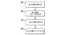
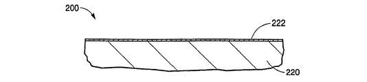
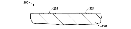
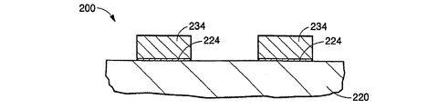
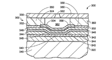
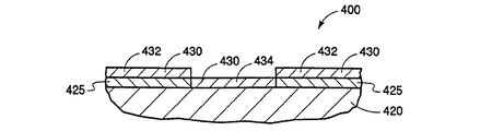
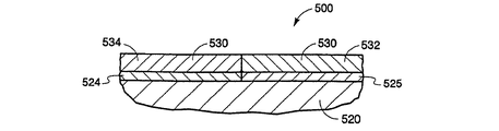
【解決手段】 本発明の方法は、第1の層(222、420)の第1の層領域(224、324、524)上に、及び第2の層(220)の第2の層領域上に配置されるタンタル層(230、330、430、530)を作り出すステップ(194)を含むタンタル構造を製造する方法であって、前記タンタル層が前記第1の層領域上の実質上bcc相のタンタル領域(234、334、434、534)であり、また前記タンタル層が前記第2の層領域上の非bcc相のタンタル領域(232、332、432、532)である方法。
【選択図】 図4
Description
222 第1の層
224 第1の層領域
230 タンタル層
232 非bcc相のタンタル領域
234 bcc相のタンタル領域
Claims (15)
- 第1の層(222、420)の第1の層領域(224、324、524)上に、及び第2の層(220)の第2の層領域上に配置されるタンタル層(230、330、430、530)を作り出すステップ(194)を含むタンタル構造を製造する方法であって、
前記タンタル層が前記第1の層領域上の実質上bcc相のタンタル領域(234、334、434、534)であり、また前記タンタル層が前記第2の層領域上の非bcc相のタンタル領域(232、332、432、532)である方法。 - 前記タンタル層を作り出すステップが、さらに、いずれも圧縮残留応力を有する実質上bcc相のタンタル領域と非bcc相のタンタル領域とを作り出すステップを含む請求項1に記載の方法。
- 前記タンタル層を作り出すステップが、さらに、前記実質上bcc相のタンタル領域及び前記非bcc相のタンタル領域が本質的に連続しているタンタル薄膜を形成するタンタル層を作り出すステップを含む請求項1に記載の方法。
- マスクを利用することなく、前記非bcc相のタンタル領域を選択的にエッチングするステップをさらに含む請求項1に記載の方法。
- 前記タンタル層を作り出すステップが、さらに、前記実質上bcc相のタンタル領域及び前記非bcc相のタンタル領域が抵抗率を有し、前記実質上bcc相のタンタル領域の前記抵抗率が、前記非bcc相のタンタル領域の前記抵抗率の約10分の1である前記タンタル層を作り出すステップを含む請求項1に記載の方法。
- 前記タンタル層を作り出すステップの前に、前記第1の層領域を洗浄するステップをさらに含む請求項1に記載の方法。
- 前記第2の層(348)を作り出すステップ、
基板と前記第1の層との間に配置される誘電体層(346)を作り出すステップ、
前記基板と前記第1の層との間に配置される抵抗器層(342)を作り出すステップ、
前記タンタル層上に配置されるチャンバ層(350)を作り出すステップ、
前記チャンバ層内に流体吐出チャンバ(352)を形成するステップ、
前記チャンバ層上に配置されるノズル層(360)を作り出すステップ、
前記チャンバ層内に形成されている流体吐出チャンバと流体連通する少なくとも1つのノズル(362)を形成するステップ
をさらに含む請求項1に記載の方法。 - 前記第1の層を作り出すステップであって、当該第1の層がbcc相のタンタルを形成する基板(420)である前記第1の層を作り出すステップ、
前記bcc相のタンタルを形成する基板上に非bcc相のタンタルを形成する層(425)を付着するステップをさらに含む請求項1に記載の方法。 - 前記第1の層を作り出すステップをさらに含み、当該第1の層が、ニオブ、アルミニウム、チタン、窒化タンタル、窒化アルミニウム、窒化ニオブ、窒化チタン、それらの混合物からなるグループより選択される材料を含む請求項1に記載の方法。
- 非bcc相のタンタル領域(232、332、432、532)に隣接した実質上bcc相のタンタル領域(234、334、434、534)を有するタンタル層を含む装置であって、
前記実質上bcc相のタンタル領域及び前記非bcc相のタンタル領域がそれぞれ圧縮残留応力を有する装置。 - 基板(320)と、
前記基板上に配置されているタンタル層(230、330、430、530)と、
前記基板と前記タンタル層の間に配置されているbcc相のタンタルを形成する領域(224、324、524)であって、前記タンタル層と接触しているbcc相のタンタルを形成する領域(224、324、524)とを含む装置であって、
前記タンタル層が前記bcc相のタンタルを形成する領域と接触している場所において、前記タンタル層が実質上bcc相のタンタル領域(234、334、434、534)を形成している装置。 - 前記タンタル層が前記bcc相のタンタルを形成する領域と接触していない場所において、前記タンタル層が非bcc相のタンタル層(232、332、432、532)を形成している請求項11に記載の装置。
- 基板(320)と、
前記基板の上方あるいは前記基板上に配置されているタンタル層(230、330、430、530)を作り出す手段とを備えている装置であって、
前記タンタル層が、少なくとも1つの非bcc相のタンタル領域(232、332、432、532)と隣接する少なくとも1つの実質上bcc相のタンタル領域(234、334、434、534)を有する装置。 - 犠牲層を選択的に除去し、自立式のタンタル層を形成する手段をさらに備えている請求項13に記載の装置。
- 前記少なくとも1つの非bcc相のタンタル領域を選択的にエッチングする手段をさらに備えている請求項13に記載の装置。
Applications Claiming Priority (1)
| Application Number | Priority Date | Filing Date | Title |
|---|---|---|---|
| US10/825,841 US7445810B2 (en) | 2004-04-15 | 2004-04-15 | Method of making a tantalum layer and apparatus using a tantalum layer |
Publications (2)
| Publication Number | Publication Date |
|---|---|
| JP2005298975A true JP2005298975A (ja) | 2005-10-27 |
| JP4533221B2 JP4533221B2 (ja) | 2010-09-01 |
Family
ID=34934283
Family Applications (1)
| Application Number | Title | Priority Date | Filing Date |
|---|---|---|---|
| JP2005116413A Expired - Fee Related JP4533221B2 (ja) | 2004-04-15 | 2005-04-14 | タンタル層を形成する方法及びタンタル層を用いる装置 |
Country Status (3)
| Country | Link |
|---|---|
| US (1) | US7445810B2 (ja) |
| EP (1) | EP1587139A3 (ja) |
| JP (1) | JP4533221B2 (ja) |
Cited By (2)
| Publication number | Priority date | Publication date | Assignee | Title |
|---|---|---|---|---|
| JP2011187789A (ja) * | 2010-03-10 | 2011-09-22 | Seiko Epson Corp | 圧電アクチュエーターの製造方法 |
| CN111799372A (zh) * | 2020-05-15 | 2020-10-20 | 上海华力微电子有限公司 | Rram阻变结构的形成方法 |
Families Citing this family (9)
| Publication number | Priority date | Publication date | Assignee | Title |
|---|---|---|---|---|
| JP2008130982A (ja) * | 2006-11-24 | 2008-06-05 | Sumitomo Electric Ind Ltd | ウエハ収納容器内に設ける部材およびその製造方法 |
| WO2009084445A1 (ja) * | 2007-12-27 | 2009-07-09 | Canon Anelva Corporation | ドライエッチング方法、磁気抵抗効果素子とその製造方法及び製造装置 |
| FR2953068B1 (fr) * | 2009-11-24 | 2012-01-20 | Commissariat Energie Atomique | Dispositif d'affichage electronique a ecran electroluminescent, et son procede de fabrication |
| US9295153B2 (en) | 2012-11-14 | 2016-03-22 | Rohm And Haas Electronic Materials Llc | Method of manufacturing a patterned transparent conductor |
| US20150001720A1 (en) * | 2013-06-27 | 2015-01-01 | Taiwan Semiconductor Manufacturing Co., Ltd. | Interconnect Structure and Method for Forming Interconnect Structure |
| SG11201703753UA (en) * | 2014-11-19 | 2017-06-29 | Memjet Technology Ltd | Inkjet nozzle device having improved lifetime |
| WO2016144359A1 (en) * | 2015-03-12 | 2016-09-15 | Hewlett-Packard Development Company, L.P. | Printhead structure |
| WO2017111814A1 (en) * | 2015-12-26 | 2017-06-29 | Intel Corporation | Low resistance interconnect |
| US10801100B2 (en) * | 2018-09-11 | 2020-10-13 | Arizona Board Of Regents On Behalf Of Arizona State University | Multimodal microstructure material and methods of forming same |
Citations (5)
| Publication number | Priority date | Publication date | Assignee | Title |
|---|---|---|---|---|
| JPH03248568A (ja) * | 1990-02-27 | 1991-11-06 | Fuji Xerox Co Ltd | 薄膜半導体装置 |
| JPH04318934A (ja) * | 1991-04-18 | 1992-11-10 | Sharp Corp | 金属薄膜及びその製造方法 |
| JPH07226507A (ja) * | 1994-02-10 | 1995-08-22 | Fujitsu Ltd | 半導体装置及びその製造方法 |
| JPH09213961A (ja) * | 1996-01-29 | 1997-08-15 | Seiko Epson Corp | 薄膜半導体装置及びその製造方法並びに電子機器及びその製造方法 |
| JP2004525257A (ja) * | 2001-01-31 | 2004-08-19 | アプライド マテリアルズ インコーポレイテッド | ウエハ・バイアスを用いて低温アルファ・タンタル薄膜を得る方法 |
Family Cites Families (9)
| Publication number | Priority date | Publication date | Assignee | Title |
|---|---|---|---|---|
| DE3063506D1 (en) * | 1979-08-31 | 1983-07-07 | Fujitsu Ltd | A tantalum thin film capacitor and process for producing the same |
| US5221449A (en) * | 1990-10-26 | 1993-06-22 | International Business Machines Corporation | Method of making Alpha-Ta thin films |
| TW201343B (ja) * | 1990-11-21 | 1993-03-01 | Toshiba Co Ltd | |
| JPH09306334A (ja) | 1996-05-10 | 1997-11-28 | Fujitsu Ltd | フィールドエミッタ及びその製造方法 |
| US6139699A (en) | 1997-05-27 | 2000-10-31 | Applied Materials, Inc. | Sputtering methods for depositing stress tunable tantalum and tantalum nitride films |
| US6830646B2 (en) | 2000-08-30 | 2004-12-14 | Lexmark International, Inc. | Radiation curable resin layer |
| US6916398B2 (en) * | 2001-10-26 | 2005-07-12 | Applied Materials, Inc. | Gas delivery apparatus and method for atomic layer deposition |
| US7294241B2 (en) | 2003-01-03 | 2007-11-13 | Chartered Semiconductor Manufacturing Ltd. | Method to form alpha phase Ta and its application to IC manufacturing |
| US6955835B2 (en) | 2003-04-30 | 2005-10-18 | Hewlett-Packard Development Company, L.P. | Method for forming compressive alpha-tantalum on substrates and devices including the same |
-
2004
- 2004-04-15 US US10/825,841 patent/US7445810B2/en not_active Expired - Fee Related
-
2005
- 2005-03-15 EP EP20050005621 patent/EP1587139A3/en not_active Withdrawn
- 2005-04-14 JP JP2005116413A patent/JP4533221B2/ja not_active Expired - Fee Related
Patent Citations (5)
| Publication number | Priority date | Publication date | Assignee | Title |
|---|---|---|---|---|
| JPH03248568A (ja) * | 1990-02-27 | 1991-11-06 | Fuji Xerox Co Ltd | 薄膜半導体装置 |
| JPH04318934A (ja) * | 1991-04-18 | 1992-11-10 | Sharp Corp | 金属薄膜及びその製造方法 |
| JPH07226507A (ja) * | 1994-02-10 | 1995-08-22 | Fujitsu Ltd | 半導体装置及びその製造方法 |
| JPH09213961A (ja) * | 1996-01-29 | 1997-08-15 | Seiko Epson Corp | 薄膜半導体装置及びその製造方法並びに電子機器及びその製造方法 |
| JP2004525257A (ja) * | 2001-01-31 | 2004-08-19 | アプライド マテリアルズ インコーポレイテッド | ウエハ・バイアスを用いて低温アルファ・タンタル薄膜を得る方法 |
Cited By (4)
| Publication number | Priority date | Publication date | Assignee | Title |
|---|---|---|---|---|
| JP2011187789A (ja) * | 2010-03-10 | 2011-09-22 | Seiko Epson Corp | 圧電アクチュエーターの製造方法 |
| US8966729B2 (en) | 2010-03-10 | 2015-03-03 | Seiko Epson Corporation | Method for manufacturing piezoelectric actuator |
| CN111799372A (zh) * | 2020-05-15 | 2020-10-20 | 上海华力微电子有限公司 | Rram阻变结构的形成方法 |
| CN111799372B (zh) * | 2020-05-15 | 2023-03-24 | 上海华力微电子有限公司 | Rram阻变结构的形成方法 |
Also Published As
| Publication number | Publication date |
|---|---|
| US7445810B2 (en) | 2008-11-04 |
| EP1587139A3 (en) | 2006-05-24 |
| EP1587139A2 (en) | 2005-10-19 |
| JP4533221B2 (ja) | 2010-09-01 |
| US20050233159A1 (en) | 2005-10-20 |
Similar Documents
| Publication | Publication Date | Title |
|---|---|---|
| KR100857629B1 (ko) | 에칭된 트렌치로부터 폴리머 코팅의 제거 방법 | |
| JP4533221B2 (ja) | タンタル層を形成する方法及びタンタル層を用いる装置 | |
| TWI281442B (en) | Ink jet recording head and producing method therefor | |
| JP6873836B2 (ja) | 液体吐出ヘッドの製造方法 | |
| US9085152B2 (en) | Etching piezoelectric material | |
| US7240433B2 (en) | Method of fabricating a thermal inkjet head having a symmetrical heater | |
| JP3480235B2 (ja) | インクジェットプリンタヘッドおよびその製造方法 | |
| JP4979793B2 (ja) | 液体吐出ヘッド用基板の製造方法 | |
| US9676193B2 (en) | Substrate processing method and method of manufacturing substrate for liquid discharge head including forming hole in substrate by dry etching | |
| US11081349B2 (en) | Method of forming film on substrate and method of manufacturing liquid ejection head | |
| RU2422289C1 (ru) | Способ изготовления головки для выпуска жидкости | |
| JP5224929B2 (ja) | 液体吐出記録ヘッドの製造方法 | |
| TWI243102B (en) | Manufacturing method of ink jet recording head and ink jet recording head manufactured by manufacturing method | |
| JP2007160625A (ja) | シリコン基板のエッチング方法、インクジェット記録ヘッドおよびその製造方法 | |
| TWI220415B (en) | Fluid eject device and method of fabricating the same | |
| TW200848273A (en) | Ink jet print head manufacturing method and ink jet print head | |
| TWI271320B (en) | Monolithic fluid injection device and method of manufacturing the same | |
| US7767103B2 (en) | Micro-fluid ejection assemblies | |
| TW504769B (en) | Forming method of piezoelectric ink jet chip | |
| JP2025108074A (ja) | 液体吐出ヘッド及び液体吐出ヘッドの製造方法 | |
| KR100467886B1 (ko) | 잉크젯프린터헤드및그제조방법 | |
| JP2007144915A (ja) | 液滴吐出ヘッドの製造方法およびパターン形成方法 | |
| JP2006225745A (ja) | 薄膜素子の構造および製造方法 | |
| JPH11170548A (ja) | インクジェットプリンターの印字ヘッドの製造方法 | |
| JP2008302586A (ja) | インクジェット記録ヘッドの製造方法 |
Legal Events
| Date | Code | Title | Description |
|---|---|---|---|
| A977 | Report on retrieval |
Free format text: JAPANESE INTERMEDIATE CODE: A971007 Effective date: 20080328 |
|
| A131 | Notification of reasons for refusal |
Free format text: JAPANESE INTERMEDIATE CODE: A131 Effective date: 20080909 |
|
| A601 | Written request for extension of time |
Free format text: JAPANESE INTERMEDIATE CODE: A601 Effective date: 20081209 |
|
| A602 | Written permission of extension of time |
Free format text: JAPANESE INTERMEDIATE CODE: A602 Effective date: 20081212 |
|
| A521 | Request for written amendment filed |
Free format text: JAPANESE INTERMEDIATE CODE: A523 Effective date: 20090309 |
|
| A131 | Notification of reasons for refusal |
Free format text: JAPANESE INTERMEDIATE CODE: A131 Effective date: 20090728 |
|
| A601 | Written request for extension of time |
Free format text: JAPANESE INTERMEDIATE CODE: A601 Effective date: 20091028 |
|
| A602 | Written permission of extension of time |
Free format text: JAPANESE INTERMEDIATE CODE: A602 Effective date: 20091102 |
|
| A521 | Request for written amendment filed |
Free format text: JAPANESE INTERMEDIATE CODE: A523 Effective date: 20100126 |
|
| TRDD | Decision of grant or rejection written | ||
| A01 | Written decision to grant a patent or to grant a registration (utility model) |
Free format text: JAPANESE INTERMEDIATE CODE: A01 Effective date: 20100601 |
|
| A01 | Written decision to grant a patent or to grant a registration (utility model) |
Free format text: JAPANESE INTERMEDIATE CODE: A01 |
|
| A61 | First payment of annual fees (during grant procedure) |
Free format text: JAPANESE INTERMEDIATE CODE: A61 Effective date: 20100611 |
|
| R150 | Certificate of patent or registration of utility model |
Free format text: JAPANESE INTERMEDIATE CODE: R150 |
|
| FPAY | Renewal fee payment (event date is renewal date of database) |
Free format text: PAYMENT UNTIL: 20130618 Year of fee payment: 3 |
|
| R250 | Receipt of annual fees |
Free format text: JAPANESE INTERMEDIATE CODE: R250 |
|
| R250 | Receipt of annual fees |
Free format text: JAPANESE INTERMEDIATE CODE: R250 |
|
| LAPS | Cancellation because of no payment of annual fees |