JP2005347364A - Extendable piezoelectric element - Google Patents
Extendable piezoelectric element Download PDFInfo
- Publication number
- JP2005347364A JP2005347364A JP2004162802A JP2004162802A JP2005347364A JP 2005347364 A JP2005347364 A JP 2005347364A JP 2004162802 A JP2004162802 A JP 2004162802A JP 2004162802 A JP2004162802 A JP 2004162802A JP 2005347364 A JP2005347364 A JP 2005347364A
- Authority
- JP
- Japan
- Prior art keywords
- piezoelectric element
- electrode layer
- substrate
- thin film
- crystal thin
- Prior art date
- Legal status (The legal status is an assumption and is not a legal conclusion. Google has not performed a legal analysis and makes no representation as to the accuracy of the status listed.)
- Pending
Links
Images

Landscapes
- Measuring Fluid Pressure (AREA)
Abstract
【課題】伸縮弾性を有する基板を伸長させても電極層が容易に切断することなく、高い信頼性を持って圧力の検出ができる伸縮可能な圧電素子を提供すること。
【解決手段】 伸縮弾性を有する基板2の片面側又は両面側に基板を伸長させた状態で、電極層3及び圧電体結晶薄膜1が形成されている伸縮可能な圧電素子Aである。
また、伸縮弾性を有する基板2の片面側又は両面側に、伸縮弾性を有する電極層3及び圧電体結晶薄膜1が形成された伸縮可能な圧電素子Aである。
そして、電極層3は、導電ペースト、導電性ゴム、導電性高分子等が採用される。
【選択図】 図1
An object of the present invention is to provide a stretchable piezoelectric element capable of detecting pressure with high reliability without easily cutting an electrode layer even when a substrate having stretch elasticity is stretched.
A stretchable piezoelectric element A in which an electrode layer 3 and a piezoelectric crystal thin film 1 are formed in a state where the substrate is extended on one side or both sides of a stretchable elastic substrate 2.
Further, the piezoelectric element A is a stretchable piezoelectric element A in which an electrode layer 3 having a stretch elasticity and the piezoelectric crystal thin film 1 are formed on one side or both sides of a substrate 2 having a stretch elasticity.
The electrode layer 3 is made of conductive paste, conductive rubber, conductive polymer, or the like.
[Selection] Figure 1
Description
本発明は、伸縮弾性を有する基板の片面側又は両面側に圧電体結晶薄膜や電極層が形成された伸縮可能な圧電素子に関する。
特に、圧力の検出、アクチュエータ、ロボットの人工皮膚等に用いるのに適した伸縮可能な圧電素子に関する。
The present invention relates to a stretchable piezoelectric element in which a piezoelectric crystal thin film or an electrode layer is formed on one side or both sides of a substrate having stretch elasticity.
In particular, the present invention relates to a stretchable piezoelectric element suitable for use in pressure detection, an actuator, an artificial skin of a robot, and the like.
従来、圧力センサーとして、圧力によって形状が変化する性質を利用したものが多く用いられている。
具体的には、金属ダイヤフラムの表面に歪ゲージを貼り付け抵抗値の変化を検出するものや、ダイヤフラムと歪ゲージをシリコーン半導体で一体形成したものがある。
更に高分子中に導電性粒子を分散させ変形による抵抗値変化を検出するものや、また圧電効果(ピエゾ効果)を利用した圧電素子が知られている。
Conventionally, many pressure sensors utilizing the property that the shape changes with pressure are used.
Specifically, there are a type in which a strain gauge is attached to the surface of a metal diaphragm to detect a change in resistance value, and a type in which the diaphragm and the strain gauge are integrally formed of a silicone semiconductor.
Furthermore, there are known ones in which conductive particles are dispersed in a polymer to detect a change in resistance value due to deformation, and piezoelectric elements utilizing a piezoelectric effect (piezo effect).
ところでこのうちの圧電素子は、圧電体と電極を一体化したもので比較的、簡単な構造であることから、圧力センサーとして種々の分野で利用されている。
しかし、変形しない剛直化した圧電素子は、例えば人体やロボット等の複雑な形状をした被検体に十分適用することはできない。
そのために、いわゆる可撓性を有する圧電素子が開発されている(例えば、特許文献1参照)。
By the way, the piezoelectric element of these is a structure in which a piezoelectric body and an electrode are integrated and has a relatively simple structure, and thus is used in various fields as a pressure sensor.
However, a rigid piezoelectric element that does not deform cannot be sufficiently applied to a subject having a complicated shape such as a human body or a robot.
Therefore, a so-called flexible piezoelectric element has been developed (see, for example, Patent Document 1).
特に、可撓性機能を与えるために可撓性を有する基板に圧電体結晶薄膜が形成された圧電素子も提供されている(例えば、特許文献2参照)。 In particular, there is also provided a piezoelectric element in which a piezoelectric crystal thin film is formed on a flexible substrate to provide a flexible function (see, for example, Patent Document 2).
しかしながら、上述したような基板に可撓性を持たせた従来の圧電素子では、比較的複雑な形状の被検体には適用可能であるが、伸縮変形等の動きのある被検体に対しての適用が困難であった。 圧電素子が伸長した場合には、特に電極が十分に追従できず、極端には断線してしまう危険があった。
すなわち、従来の圧電素子では、伸縮変形が生じ易い被検体の圧力センサーとしては高い信頼性を持って適用することが困難であったのである。
However, the conventional piezoelectric element in which the substrate is flexible as described above can be applied to a subject having a relatively complicated shape, but it can be applied to a subject having movement such as expansion and contraction. It was difficult to apply. When the piezoelectric element is elongated, there is a risk that the electrode cannot sufficiently follow, and is extremely disconnected.
In other words, the conventional piezoelectric element is difficult to apply with high reliability as a pressure sensor for a subject that easily undergoes stretching and deformation.
本発明は、かかる背景技術をもとになされたもので、上記の背景技術の問題点を克服するためになされたものである。
すなわち、本発明は、伸縮弾性を有する基板を伸長させても電極層が容易に切断することなく、高い信頼性を持って圧力の検出ができる伸縮可能な圧電素子を提供することを目的とする。
The present invention has been made on the basis of such background technology, and has been made to overcome the above-described problems of the background technology.
That is, an object of the present invention is to provide a stretchable piezoelectric element capable of detecting pressure with high reliability without easily cutting an electrode layer even when a substrate having stretch elasticity is stretched. .
かくして、本発明者は、このような課題背景に対して鋭意研究を重ねた結果、伸縮弾性を有する基板の片面側又は両面側に伸縮弾性を有する電極層を形成することにより、或いは伸縮弾性を有する基板を伸長させた状態で電極層を形成することにより、上記の問題点を解決することができることを見出し、この知見に基づいて本発明を完成させたものである。 Thus, as a result of earnest research on the background of such problems, the present inventor has formed an electrode layer having stretch elasticity on one side or both sides of a substrate having stretch elasticity, or has provided stretch elasticity. The inventors have found that the above problems can be solved by forming an electrode layer in a state where a substrate having the substrate is extended, and the present invention has been completed based on this finding.
すなわち、本発明は、(1)、伸縮弾性を有する基板の片面側又は両面側に基板を伸長させた状態で、電極層及び圧電体結晶薄膜が形成されている伸縮可能な圧電素子に存する。 That is, the present invention resides in (1) a stretchable piezoelectric element in which an electrode layer and a piezoelectric crystal thin film are formed in a state where the substrate is stretched on one side or both sides of the stretchable substrate.
また、本発明は、(2)、伸縮弾性を有する基板の片面側又は両面側に、伸縮弾性を有する電極層及び圧電体結晶薄膜が形成された伸縮可能な圧電素子に存する。 The present invention also resides in (2) a stretchable piezoelectric element in which an electrode layer and a piezoelectric crystal thin film having stretch elasticity are formed on one side or both sides of a substrate having stretch elasticity.
また、本発明は、(3)、前記伸縮弾性を有する基板は、合繊樹脂を主成分として含むものである上記(1)又は(2)に記載の伸縮可能な圧電素子に存する。 Further, the present invention resides in (3) the stretchable piezoelectric element according to the above (1) or (2), wherein the substrate having stretch elasticity includes a synthetic fiber resin as a main component.
また、本発明は、(4)、前記伸縮弾性を有する基板は、エラストマーを主成分として含む上記(1)又は(2)に記載の伸縮可能な圧電素子に存する。 In addition, the present invention resides in (4) the stretchable piezoelectric element according to (1) or (2), wherein the substrate having stretch elasticity includes an elastomer as a main component.
また、本発明は、(5)、前記エラストマーとして、シリコーンゴムを使用する上記(3)に記載の伸縮可能な圧電素子に存する。 Moreover, this invention exists in the piezoelectric element which can be expanded / contracted as described in said (3) which uses silicone rubber as said elastomer (5).
また、本発明は、(6)、前記圧電体結晶薄膜は、複合酸化物を主成分として含むものである上記(1)又は(2)に記載の伸縮可能な圧電素子に存する。 The present invention also resides in (6) the expandable / contractible piezoelectric element according to (1) or (2), wherein the piezoelectric crystal thin film contains a complex oxide as a main component.
また、本発明は、(7)、前記複合酸化物として、ジルコンチタン酸鉛(PZT)、ニオブ酸リチウム、又はチタン酸バリウムのいずれか1種である上記(5)に記載の伸縮可能な圧電素子に存する。 The present invention also provides (7) the expandable / contractable piezoelectric element according to (5), wherein the composite oxide is any one of lead zirconate titanate (PZT), lithium niobate, or barium titanate. It exists in the element.
また、本発明は、(8)、前記圧電体結晶薄膜は、ウルツ鉱型構造の化合物を主成分として含むものである上記(1)又は(2)に記載の伸縮可能な圧電素子に存する。 The present invention also resides in (8) the expandable / contractible piezoelectric element according to (1) or (2), wherein the piezoelectric crystal thin film contains a compound having a wurtzite structure as a main component.
また、本発明は、(9)、前記ウルツ鉱型構造の化合物として、窒化アルミニウム、酸化亜鉛、ヨウ化銀、硫化亜鉛、硫化カドミウム、窒化ガリウムのいずれか1種である上記(7)に記載の伸縮可能な圧電素子に存する。 Further, the present invention is as described in (9) above, wherein the compound having the wurtzite structure is any one of aluminum nitride, zinc oxide, silver iodide, zinc sulfide, cadmium sulfide, and gallium nitride. The piezoelectric element can be expanded and contracted.
また、本発明は、(10)、前記電極層は、金属又は金属酸化物を主成分として含む上記(1)又は(2)に記載の伸縮可能な圧電素子に存する。 Further, the present invention resides in (10), the expandable / contractible piezoelectric element according to (1) or (2), wherein the electrode layer contains a metal or a metal oxide as a main component.
また、本発明は、(11)、前記電極層は、導電ペースト、導電性ゴム、又は導電性高分子いずれか1種を主成分として含むものよりなる上記(2)に記載の伸縮可能な圧電素子に存する。 The present invention also relates to (11), wherein the electrode layer comprises the conductive paste, the conductive rubber, or the conductive polymer as a main component, and the stretchable piezoelectric device according to the above (2). It exists in the element.
なお、本発明の目的に添ったものであれば、上記(1)から(11)を適宜組み合わせた構成も採用可能である。 In addition, as long as the objective of this invention is met, the structure which combined said (1) to (11) suitably is also employable.
本発明の圧電素子によれば、伸縮弾性を有する基板の片面側又は両面側に基板を伸長させた状態で、電極層及び圧電体結晶薄膜が形成されているので、通常の状態において電極層及び圧電体結晶薄膜は圧縮荷重を受けており、圧電素子の基板が伸長しても、圧縮荷重が解放されるだけであり、電極層や圧電体結晶薄膜が切断されるようなことはなく、高い信頼性を持って圧力の検出を行うことができる。 According to the piezoelectric element of the present invention, since the electrode layer and the piezoelectric crystal thin film are formed in a state where the substrate is stretched on one side or both sides of the substrate having stretch elasticity, the electrode layer and the piezoelectric layer are formed in a normal state. The piezoelectric crystal thin film is subjected to a compressive load. Even if the substrate of the piezoelectric element is stretched, the compressive load is only released, and the electrode layer and the piezoelectric crystal thin film are not cut and are high Pressure can be detected with reliability.
また、本発明の圧電素子によれば、伸縮弾性を有する基板の片面側又は両面側に、伸縮弾性を有する電極層及び圧電体結晶薄膜が形成されているので、同様に、圧電素子の基板が伸長しても、圧電体結晶薄膜や電極層が追従して伸縮することができ、電極層が容易に切断されることはなく、高い信頼性を持って圧力の検出を行うことができる。 Further, according to the piezoelectric element of the present invention, the electrode layer and the piezoelectric crystal thin film having stretch elasticity are formed on one side or both sides of the substrate having stretch elasticity. Even when stretched, the piezoelectric crystal thin film and the electrode layer can follow and expand and contract, and the electrode layer is not easily cut, and pressure can be detected with high reliability.
以下、本発明を実施するための最良の形態を図面に基づいて説明する。
(第1実施形態)
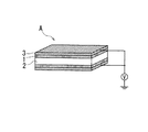
図1は、本発明の第1実施形態に係る圧電素子Aを示している。
この第1実施形態の圧電素子Aは、伸縮弾性を有する基板2上に圧電体1である圧電体結晶薄膜が形成されている。
圧電体結晶薄膜1の両面には電極層3が形成されている。
基板2として圧電素子Aの伸縮性を発現する礎となる部分であり、その基板2の材料には、伸縮弾性の顕著な高分子物質であるエラストマーを用いることが好ましい。
エラストマーの具体例としては、例えば、架橋した天然ゴムや合成ゴム、シリコーンゴム等が挙げられる。
Hereinafter, the best mode for carrying out the present invention will be described with reference to the drawings.
(First embodiment)
FIG. 1 shows a piezoelectric element A according to the first embodiment of the present invention.
In the piezoelectric element A of the first embodiment, a piezoelectric crystal thin film that is the
The
Specific examples of the elastomer include, for example, cross-linked natural rubber, synthetic rubber, and silicone rubber.
この圧電体結晶薄膜1を基板2上に形成するに当たっては、先ず、基板2をその面方向に伸ばした状態で基板2上に電極層3を形成する。
次いで、電極層3を形成した後、基板2を伸長させたままの状態で、圧電体結晶薄膜1を形成する。
この圧電体結晶薄膜1の上面にも、同様の方法で電極層3を形成する。
In forming the piezoelectric crystal
Next, after the
The
圧電体結晶薄膜1の形成方法としては、スパッタリング法、レーザーアブレージョン法、イオンプレーティング法、或いはCVD法、MOCVD法、水熱合成法等が知られており、その中から好ましいものを選ぶ。
例えば水熱合成法によれば、伸縮弾性を有する基板2に圧電体結晶薄膜1を形成することが容易に可能であり、伸縮性に加え圧電性能の優れた圧電素子Aが提供される。
As a method for forming the piezoelectric crystal
For example, according to the hydrothermal synthesis method, the piezoelectric crystal
圧電体結晶薄膜1としては、圧電特性を備えるものであれば種々のものが採用されるが、水熱合成法を用いる場合は、ペロブスカイト(ABO3)構造の複合酸化物がある。
A variety of piezoelectric crystal
そして、上記Aサイトとしては、通常、Pb,Ba,Ca,Sr,La,Li,Biの中から選択される少なくとも1種の元素が採用される。
上記Bサイトとしては、Ti単独か、或いはZr,Zn,Ni,Mg,Co,W,Nb,Sb,Ta,Feの中から選択される少なくとも1種の元素とTiとの複合物が挙げられる。
このような複合酸化物の具体例としては、Pb(Zr,Ti)O3、PbTiO3、BaTiO3、SrTiO3、(Pb,La)(Zr,Ti)O3、LiNbO3等が挙げられる。
And as said A site, the at least 1 sort (s) of element normally selected from Pb, Ba, Ca, Sr, La, Li, and Bi is employ | adopted.
Examples of the B site include Ti alone or a composite of Ti and at least one element selected from Zr, Zn, Ni, Mg, Co, W, Nb, Sb, Ta, and Fe. .
Specific examples of such complex oxides include Pb (Zr, Ti) O3, PbTiO3, BaTiO3, SrTiO3, (Pb, La) (Zr, Ti) O3, and LiNbO3.
また、圧電体結晶薄膜1は、上述した材料とは異なり、ウルツ鉱型構造の化合物を主成分とする材料にしても良い。
ウルツ鉱型構造としては具体的には、例えば、窒化アルミニウム、酸化亜鉛、ヨウ化銀、硫化亜鉛、硫化カドミウム、窒化ガリウム等があり、これらの中から1種選択すればよい。
ところで圧電体結晶薄膜1の厚みは、通常、0.1〜100μm、特に0.5〜30μmに設定することが好適である。
すなわち、厚みが0.1μm未満では、例えばセンサーやアクチュエータ等に用いた場合に十分な出力が得られにくく、逆に100μmを超えると弾性を有する基板2を用いているにもかかわらず、柔軟性が乏しくなり出力が小さくなる恐れがある。
Further, the piezoelectric crystal
Specific examples of the wurtzite structure include aluminum nitride, zinc oxide, silver iodide, zinc sulfide, cadmium sulfide, and gallium nitride. One of these may be selected.
By the way, it is preferable that the thickness of the piezoelectric crystal
That is, when the thickness is less than 0.1 μm, it is difficult to obtain a sufficient output when used for, for example, a sensor or an actuator. There is a risk that the output will become small due to the lack of power.
さて電極層3の材料としては、Al,Ni,Pt,Au,Ag,Cu等の金属製の導電材料を用いることができ、またそれらの酸化物(金属酸化物)も採用できる。
特に、伸縮弾性を有する電極層3としては、導電ペースト、導電性ゴム、又は導電性合成樹脂が採用される。
この電極層3は、基板2又は圧電体結晶薄膜1の表面に被覆することで形成する。
As the material of the
In particular, as the
The
その方法は、特に限定されるものではなく、例えば塗布処理、無電解メッキ法、スパッタリング法、及び化学蒸着法等を用いることができる。
そして、電極層3の厚みは、通常、1μm以下、特に0.1μm以下に設定することが好適である。
The method is not particularly limited, and for example, a coating process, an electroless plating method, a sputtering method, a chemical vapor deposition method, or the like can be used.
And it is suitable for the thickness of the
上述した圧電素子Aは、外部から圧力を加えられると電極層3間の電位差Vや電荷が変化し、この電位差Vや電荷を計測することにより加えられた圧力を求めることができる。
このように外部から圧力を加えられた場合、基板2が伸縮弾性を有しているために、硬い基板上に形成された圧電素子に比べ圧電体結晶薄膜1は大きな歪を生じ、電極層3間に発生する電位差や電荷が大きくなるという長所がある。
The piezoelectric element A described above changes the potential difference V and charge between the electrode layers 3 when pressure is applied from the outside, and the applied pressure can be obtained by measuring the potential difference V and charge.
When pressure is applied from the outside as described above, the piezoelectric crystal
この第1実施形態では、伸縮弾性を有する基板2の片面側に基板2を伸ばした状態で、電極層3及び圧電体結晶薄膜1が形成されたので、通常の状態において電極層3及び圧電体結晶薄膜1は圧縮荷重を受けており、圧電素子Aを使用中に基板2が多少伸長しても、圧縮荷重が解放されるだけである。
そのため電極層3としても伸縮弾性を有するものではなくてもよい。
電極層3や圧電体結晶薄膜1が切断されるようなことはなく、高い信頼性を持って圧力の検出を行うことができる。
以上述べたものは、伸縮弾性を有する基板2を伸長した状態で、基板2の片面側又は両面側に電極層3や圧電体結晶薄膜1を形成したものである。
しかし、伸縮弾性を有する基板2を伸長しない状態、すなわち通常の状態で基板2の片面側又は両面側に電極層3や圧電体結晶薄膜1を形成することも可能である。
その場合は電極層3としては、導電性ゴム又は導電性合成樹脂等の伸縮弾性を有する電極層3を使うこととなる。
尚、圧電体結晶薄膜1は、その構造上、基板2の伸長にも追従していくことができる。
以下、第2実施の形態から第6実施の形態においても同様である。
In the first embodiment, since the
Therefore, the
The
In the above description, the
However, it is also possible to form the
In this case, as the
The piezoelectric crystal
Hereinafter, the same applies to the second to sixth embodiments.
(第2実施形態)
図2は、本発明の第2実施形態に係る圧電素子Aを示している。
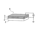
この第2実施形態の圧電素子Aは、上記第1実施の形態における圧電体結晶薄膜1及び電極層3が基板2を介して対称的に反対面にも形成されている構造を有する。
具体的には、基板2の上下面の各々に電極層3が形成され、この各電極層3上に更に圧電体結晶薄膜1及びもう1層の電極層3が形成されている。
(Second Embodiment)
FIG. 2 shows a piezoelectric element A according to the second embodiment of the present invention.
The piezoelectric element A according to the second embodiment has a structure in which the piezoelectric crystal
Specifically, an
この第2実施形態では、第1実施形態と同様の効果を奏する。
更に、この第2実施形態では、基板2の両面に圧電体である圧電体結晶薄膜1を形成するようにしたので、基板2の上下方向に同程度の振動を加えることができ、左右対称に振動を伝播させることが望まれる装置にとって好適である。
また、一方の圧電体結晶薄膜1にクラック等が生じて機能が低下しても、他方の圧電体結晶薄膜1が機能するために、フェールセーフとなり安全性が向上する。
The second embodiment has the same effect as the first embodiment.
Furthermore, in the second embodiment, since the piezoelectric crystal
Further, even if a crack or the like occurs in one piezoelectric crystal
(第3実施形態)
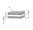
図3は、本発明の第3実施形態に係る圧電素子Aを示している。
この第3実施形態の圧電素子Aは第1及び第2実施形態の圧電素子と比べて、電極層3が1層少ない点で相違する。
すなわち、圧電素子Aに外部から圧力を加えられると、電極層3と接地電位部との間の電位差Vや
電荷は変化し、この電位差Vや電荷を計測することにより加えられた圧力を求めることができるのである。
(Third embodiment)
FIG. 3 shows a piezoelectric element A according to the third embodiment of the present invention.
The piezoelectric element A according to the third embodiment is different from the piezoelectric elements according to the first and second embodiments in that the number of
That is, when external pressure is applied to the piezoelectric element A, the potential difference V and charge between the
(第4実施形態)
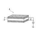
図4は、本発明の第4実施形態に係る圧電素子Aを示している。
この第4実施形態の圧電素子Aは、上記第3実施の形態における圧電体結晶薄膜1及び電極層3が基板2を介して対称的に反対面にも形成されている構造を有する。
具体的には、基板2の上下面の各々に電極層3が形成され、この各電極層3上に更に圧電体結晶薄膜1が形成されている。
(Fourth embodiment)
FIG. 4 shows a piezoelectric element A according to the fourth embodiment of the present invention.
The piezoelectric element A of the fourth embodiment has a structure in which the piezoelectric crystal
Specifically, an
一方の圧電体結晶薄膜1や電極3にクラック等が生じて機能が低下しても、他方の圧電体結晶薄膜1や電極3が機能するために安全性が向上する。
Even if a crack or the like occurs in one piezoelectric crystal
(第5実施形態)
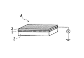
図5は、本発明の第5実施形態に係る圧電素子Aを示している。
この第5実施形態の圧電素子Aは第3実施形態の圧電素子と比べて、電極層3と圧電体結晶薄膜1との位置が入れ替わっている点で相違する。
圧電素子Aに外部から圧力を加えられると、電極層3と接地電位部と間の電位差Vや電荷が変化し、この電位差Vや電荷を計測することにより加えられた圧力を求めることができる。
(Fifth embodiment)
FIG. 5 shows a piezoelectric element A according to the fifth embodiment of the present invention.
The piezoelectric element A according to the fifth embodiment is different from the piezoelectric element according to the third embodiment in that the positions of the
When pressure is applied to the piezoelectric element A from the outside, the potential difference V and charge between the
(第6実施形態)
図6は、本発明の第6実施形態に係る圧電素子Aを示している。
この第6実施形態の圧電素子Aは、上記第5実施の形態における圧電体結晶薄膜1及び電極層3が基板2を介して対称的に反対面にも形成されている構造を有する。
具体的には、基板2の上下面の各々に圧電体結晶薄膜1が形成され、この各圧電体結晶薄膜1上に更に電極層3が形成されている。
一方の圧電体結晶薄膜1や電極3にクラック等が生じて機能が低下しても、他方の圧電体結晶薄膜1や電極3が機能するために安全性が向上する。
(Sixth embodiment)
FIG. 6 shows a piezoelectric element A according to a sixth embodiment of the present invention.
The piezoelectric element A of the sixth embodiment has a structure in which the piezoelectric crystal
Specifically, the piezoelectric crystal
Even if a crack or the like occurs in one piezoelectric crystal
以上、本発明を説明してきたが、本発明は上述した第1〜第6実施形態にのみ限定されるものではなく、その本質を逸脱しない範囲で、他の種々の変形が可能であることはいうまでもない。
例えば、上述した実施形態では、弾性を有する基板2の片面側又は両面側に基板2を伸ばした状態で、伸縮弾性を有する電極層3を形成することも当然可能である。
Although the present invention has been described above, the present invention is not limited to the first to sixth embodiments described above, and various other modifications can be made without departing from the essence thereof. Needless to say.
For example, in the embodiment described above, it is naturally possible to form the
以下、実施例を挙げて説明するが、本発明は、当然、これらの実施例によって限定されるものではない。 Hereinafter, although an example is given and explained, the present invention is naturally not limited by these examples.
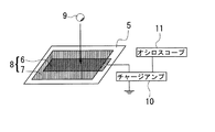
図7は、本発明の圧電素子8が作動することを確認するための第1の実験装置を示している。
図に示すように、伸縮弾性を有する基板であるシリコーンゴムシート5上には、該シリコーンゴムシート5を伸長させた状態にして白金電極層6と圧電体結晶薄膜である窒化アルミニウム薄膜7を順次RFマグネトロンスパッタリング法を用いて成膜し圧電素子8を形成した。
窒化アルミニウム薄膜7は白金電極層6を完全には覆っておらず、一部露出した状態にされている。
FIG. 7 shows a first experimental apparatus for confirming that the
As shown in the figure, a
The aluminum nitride thin film 7 does not completely cover the
このようにして作成した圧電素子8の白金電極層6の部分に、質量1.2gの錘9を高さ5cmの所から落下させ、白金電極層6と接地電位部との間の電荷を変化させた。
この変化の電気的出力をチャージアンプ10で増幅させ、オシロスコープ11により測定した結果、440pCの電荷が検出された。
またシリコーンゴムシート5に繰り返し引っ張り力を加えて(200回)圧電素子8を観察したところ、白金電極層6や窒化アルミニウム薄膜7には亀裂が全く生じていないことが分かった。
A
The electrical output of this change was amplified by the
Further, when a tensile force was repeatedly applied to the silicone rubber sheet 5 (200 times) and the
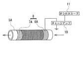
図8は、本発明の圧電素子が作動することを確認するための第2の実験装置を示している。
図に示すように、シリコーンゴムチューブ5A上には、導電性ゴム電極層6Aと窒化アルミニウム薄膜7Aを順次RFマグネトロンスパッタリング法を用いて成膜し圧電素子8を形成した。
FIG. 8 shows a second experimental apparatus for confirming that the piezoelectric element of the present invention operates.
As shown in the drawing, a conductive
窒化アルミニウム薄膜7Aは導電性ゴム電極層6Aを完全には覆っておらず、一部露出した状態にされている。
このようにして作製した圧電素子8Aに空気をダイヤフラム式エアーポンプを用いて流した。
導電性ゴム電極層6Aと接地電位部との間で変化した電荷をチャージアンプ10で増幅させ、オシロスコープ11により測定したところ、空気圧に対応した信号が検出された。
またシリコーンゴムゴムチューブ5Aに繰り返し引っ張り力を加えて(250回)圧電素子8Aを観察したところ、導電性ゴム電極層6Aや窒化アルミニウム薄膜7Aには亀裂が全く生じていないことが分かった。
The aluminum nitride
Air was passed through the piezoelectric element 8A thus produced using a diaphragm type air pump.
When the electric charge changed between the conductive
Further, when a tensile force was repeatedly applied to the
本発明の圧電素子は、民生用電子機器、家電・住宅用電子機器、セキュリティー機器、健康器具、オートメーションファクトリ、ロボット、自動車、事務機器、その他様々な分野で圧力センサーとして利用することができる。
また、原理から見て、スピーカー、圧電リレー、超音波加工等への応用も可能である。
The piezoelectric element of the present invention can be used as a pressure sensor in various fields such as consumer electronic devices, home appliances / residential electronic devices, security devices, health appliances, automation factories, robots, automobiles, office equipment, and the like.
From the principle, application to speakers, piezoelectric relays, ultrasonic machining, etc. is also possible.
A 圧電素子
1 圧電体(圧電体結晶薄膜)
2 基板
3 電極層
5,5A シリコーンゴムシート
6 白金電極層
6A 導電性ゴム電極層
7,7A 窒化アルミニウム薄膜
8,8A 圧電素子
9 錘
10 チャージアンプ
11 オシロスコープ
V 電源
A
2
V power supply
Claims (11)
Priority Applications (1)
| Application Number | Priority Date | Filing Date | Title |
|---|---|---|---|
| JP2004162802A JP2005347364A (en) | 2004-06-01 | 2004-06-01 | Extendable piezoelectric element |
Applications Claiming Priority (1)
| Application Number | Priority Date | Filing Date | Title |
|---|---|---|---|
| JP2004162802A JP2005347364A (en) | 2004-06-01 | 2004-06-01 | Extendable piezoelectric element |
Publications (1)
| Publication Number | Publication Date |
|---|---|
| JP2005347364A true JP2005347364A (en) | 2005-12-15 |
Family
ID=35499481
Family Applications (1)
| Application Number | Title | Priority Date | Filing Date |
|---|---|---|---|
| JP2004162802A Pending JP2005347364A (en) | 2004-06-01 | 2004-06-01 | Extendable piezoelectric element |
Country Status (1)
| Country | Link |
|---|---|
| JP (1) | JP2005347364A (en) |
Cited By (12)
| Publication number | Priority date | Publication date | Assignee | Title |
|---|---|---|---|---|
| JP2007173226A (en) * | 2005-11-28 | 2007-07-05 | Osaka Univ | Rubber material and method for producing rubber material |
| JP2007287739A (en) * | 2006-04-12 | 2007-11-01 | Seiko Epson Corp | Piezoelectric material and piezoelectric element |
| JP2011071363A (en) * | 2009-09-28 | 2011-04-07 | Murata Mfg Co Ltd | Actuator array |
| CN102163687A (en) * | 2010-12-10 | 2011-08-24 | 清华大学 | High-voltage electrical response zinc oxide flexible pressure sensor and manufacturing method thereof |
| JP2014208534A (en) * | 2008-08-29 | 2014-11-06 | ミシュラン ルシェルシュ エ テクニーク ソシエテ アノニム | 1-D tire patch device and method |
| JP2015515612A (en) * | 2012-03-15 | 2015-05-28 | フォルシュングスツェントルム・ユーリッヒ・ゲゼルシャフト・ミット・ベシュレンクテル・ハフツング | SENSOR DEVICE COMPRISING CARRIER SUBSTRATE AND FERROELECTRIC LAYER, AND MANUFACTURING METHOD AND USE THEREOF |
| US9773969B2 (en) * | 2015-05-28 | 2017-09-26 | The Board Of Trustees Of The Leland Stanford Junior University | Electrostrictive element manufacturing method |
| US9871183B2 (en) | 2015-05-28 | 2018-01-16 | The Board Of Trustees Of The Leland Stanford Junior University | Electrostrictive element |
| JPWO2018047878A1 (en) * | 2016-09-06 | 2019-06-24 | 積水化学工業株式会社 | Piezoelectric sensor |
| KR20190091861A (en) * | 2018-01-29 | 2019-08-07 | 충북대학교 산학협력단 | Method and system for manufacturing copper electrode |
| WO2021243546A1 (en) * | 2020-06-02 | 2021-12-09 | 晶极光电科技股份有限公司 | Method for manufacturing multi-hole pressure sensor, and multi-hole pressure sensor |
| JP2022532365A (en) * | 2019-05-15 | 2022-07-14 | ティーディーケイ・エレクトロニクス・アクチェンゲゼルシャフト | Ferroelectric sensor |
Citations (10)
| Publication number | Priority date | Publication date | Assignee | Title |
|---|---|---|---|---|
| JPS62151733A (en) * | 1985-12-20 | 1987-07-06 | ア−・フアウ・エル ゲゼルシヤフト フイア フエアブレヌングスクラフトマシ−ネン ウント メステヒニク エム・ベ−・ハ− プロフエツサ−・ドクタ−・ドクタ−・ハ−・ツエ−・ハンス・リスト | A sensor with a flexible piezoelectric film as a measuring element and its manufacturing method |
| JPH06216422A (en) * | 1991-08-09 | 1994-08-05 | Kureha Chem Ind Co Ltd | Flexible laminated piezoelectric element |
| JPH06283777A (en) * | 1993-03-26 | 1994-10-07 | Onoda Cement Co Ltd | Multilayer piezoelectric actuater and manufacture thereof |
| JPH0774406A (en) * | 1993-01-13 | 1995-03-17 | Akihiro Fujimura | Polarized fine particle-loaded electromagnetic strain material |
| JPH0888418A (en) * | 1994-09-10 | 1996-04-02 | Korea Electron Telecommun | Piezoelectric element using ultra-thin metal film |
| JPH10256570A (en) * | 1997-03-14 | 1998-09-25 | Matsushita Electric Ind Co Ltd | Thin film device and thin film manufacturing method |
| JP2000337971A (en) * | 1999-05-27 | 2000-12-08 | Tokai Rubber Ind Ltd | Flexible sensor |
| JP2000346717A (en) * | 1999-06-03 | 2000-12-15 | Matsushita Electric Ind Co Ltd | Piezoelectric sensor, piezoelectric sensor load detection device and pinch prevention device |
| JP2001007419A (en) * | 1999-06-24 | 2001-01-12 | Tokai Rubber Ind Ltd | Actuator |
| JP2001135873A (en) * | 1999-11-08 | 2001-05-18 | Minolta Co Ltd | Piezoelectric conversion element |
-
2004
- 2004-06-01 JP JP2004162802A patent/JP2005347364A/en active Pending
Patent Citations (10)
| Publication number | Priority date | Publication date | Assignee | Title |
|---|---|---|---|---|
| JPS62151733A (en) * | 1985-12-20 | 1987-07-06 | ア−・フアウ・エル ゲゼルシヤフト フイア フエアブレヌングスクラフトマシ−ネン ウント メステヒニク エム・ベ−・ハ− プロフエツサ−・ドクタ−・ドクタ−・ハ−・ツエ−・ハンス・リスト | A sensor with a flexible piezoelectric film as a measuring element and its manufacturing method |
| JPH06216422A (en) * | 1991-08-09 | 1994-08-05 | Kureha Chem Ind Co Ltd | Flexible laminated piezoelectric element |
| JPH0774406A (en) * | 1993-01-13 | 1995-03-17 | Akihiro Fujimura | Polarized fine particle-loaded electromagnetic strain material |
| JPH06283777A (en) * | 1993-03-26 | 1994-10-07 | Onoda Cement Co Ltd | Multilayer piezoelectric actuater and manufacture thereof |
| JPH0888418A (en) * | 1994-09-10 | 1996-04-02 | Korea Electron Telecommun | Piezoelectric element using ultra-thin metal film |
| JPH10256570A (en) * | 1997-03-14 | 1998-09-25 | Matsushita Electric Ind Co Ltd | Thin film device and thin film manufacturing method |
| JP2000337971A (en) * | 1999-05-27 | 2000-12-08 | Tokai Rubber Ind Ltd | Flexible sensor |
| JP2000346717A (en) * | 1999-06-03 | 2000-12-15 | Matsushita Electric Ind Co Ltd | Piezoelectric sensor, piezoelectric sensor load detection device and pinch prevention device |
| JP2001007419A (en) * | 1999-06-24 | 2001-01-12 | Tokai Rubber Ind Ltd | Actuator |
| JP2001135873A (en) * | 1999-11-08 | 2001-05-18 | Minolta Co Ltd | Piezoelectric conversion element |
Cited By (19)
| Publication number | Priority date | Publication date | Assignee | Title |
|---|---|---|---|---|
| JP2007173226A (en) * | 2005-11-28 | 2007-07-05 | Osaka Univ | Rubber material and method for producing rubber material |
| JP2007287739A (en) * | 2006-04-12 | 2007-11-01 | Seiko Epson Corp | Piezoelectric material and piezoelectric element |
| JP2014208534A (en) * | 2008-08-29 | 2014-11-06 | ミシュラン ルシェルシュ エ テクニーク ソシエテ アノニム | 1-D tire patch device and method |
| JP2011071363A (en) * | 2009-09-28 | 2011-04-07 | Murata Mfg Co Ltd | Actuator array |
| CN102163687A (en) * | 2010-12-10 | 2011-08-24 | 清华大学 | High-voltage electrical response zinc oxide flexible pressure sensor and manufacturing method thereof |
| US9515157B2 (en) | 2012-03-05 | 2016-12-06 | Forschungszentrum Juelich Gmbh | Sensor arrangement comprising a carrier substrate and a ferroelectric layer and method for producing and using the sensor arrangement |
| JP2015515612A (en) * | 2012-03-15 | 2015-05-28 | フォルシュングスツェントルム・ユーリッヒ・ゲゼルシャフト・ミット・ベシュレンクテル・ハフツング | SENSOR DEVICE COMPRISING CARRIER SUBSTRATE AND FERROELECTRIC LAYER, AND MANUFACTURING METHOD AND USE THEREOF |
| US9871183B2 (en) | 2015-05-28 | 2018-01-16 | The Board Of Trustees Of The Leland Stanford Junior University | Electrostrictive element |
| US9773969B2 (en) * | 2015-05-28 | 2017-09-26 | The Board Of Trustees Of The Leland Stanford Junior University | Electrostrictive element manufacturing method |
| DE102016208978B4 (en) | 2015-05-28 | 2018-03-22 | Honda Motor Co., Ltd. | Electrostrictive element |
| JPWO2018047878A1 (en) * | 2016-09-06 | 2019-06-24 | 積水化学工業株式会社 | Piezoelectric sensor |
| JP7271084B2 (en) | 2016-09-06 | 2023-05-11 | 積水化学工業株式会社 | piezo sensor |
| KR20190091861A (en) * | 2018-01-29 | 2019-08-07 | 충북대학교 산학협력단 | Method and system for manufacturing copper electrode |
| KR102100550B1 (en) | 2018-01-29 | 2020-04-13 | 충북대학교 산학협력단 | Method and system for manufacturing copper electrode |
| JP2022532365A (en) * | 2019-05-15 | 2022-07-14 | ティーディーケイ・エレクトロニクス・アクチェンゲゼルシャフト | Ferroelectric sensor |
| US12209913B2 (en) | 2019-05-15 | 2025-01-28 | Tdk Electronics Ag | Piezoelectric device having a support with a neutral fiber |
| EP4498052A3 (en) * | 2019-05-15 | 2025-04-02 | TDK Electronics AG | Ferroelectric sensor |
| US12436034B2 (en) | 2019-05-15 | 2025-10-07 | Tdk Electronics Ag | Ferroelectric sensor |
| WO2021243546A1 (en) * | 2020-06-02 | 2021-12-09 | 晶极光电科技股份有限公司 | Method for manufacturing multi-hole pressure sensor, and multi-hole pressure sensor |
Similar Documents
| Publication | Publication Date | Title |
|---|---|---|
| US11165011B2 (en) | Piezoelectric element and method for manufacturing piezoelectric element | |
| Uchino | Glory of piezoelectric perovskites | |
| US20100294976A1 (en) | Composition for energy generator, storage, and strain sensor and methods of use thereof | |
| JP5019120B2 (en) | Detection sensor | |
| JP2005347364A (en) | Extendable piezoelectric element | |
| WO2007125985A1 (en) | Mechanical-electrical converting device and its manufacturing method | |
| JP3093849B2 (en) | Flexible laminated piezoelectric element | |
| JP6346693B2 (en) | Method for manufacturing piezoelectric element | |
| JP4756309B2 (en) | High sensitivity piezoelectric element | |
| Salowitz et al. | Screen printed piezoceramic actuators/sensors microfabricated on organic films and stretchable networks | |
| Inman et al. | Structural and machine design using piezoceramic materials: a guide for structural design engineers | |
| JP4736599B2 (en) | Piezoelectric element | |
| Mirshekarloo et al. | Electromechanical properties and fatigue of antiferroelectric (Pb, La)(Zr, Sn, Ti) O3 thin film cantilevers fabricated by micromachining | |
| JPH10209517A (en) | Piezoelectric element | |
| CN110832653A (en) | Vibration Sensors and Piezoelectric Components | |
| JP4803633B2 (en) | Piezoelectric detector | |
| Allamraju et al. | Studies on mechanical and electrical characteristics of PZT-5H patch | |
| JP4868532B2 (en) | Piezoelectric sensor | |
| Yeager | PZT thin films for piezoelectric MEMS mechanical energy harvesting | |
| Naik et al. | Design and simulation of underwater acoustic sensor materials | |
| Kumar et al. | Pyroelectric and piezoelectric polymers | |
| KR102813821B1 (en) | Self―powered sensor susceptible to buckling phenomenon and method of manufacturing the same | |
| Kang et al. | Piezoelectric paint sensor for impact and vibration monitoring | |
| Vucheva et al. | Comparison of the piezoelectric properties of single-layer and bilayer structures with thin films of PZT and ZnO in dynamic mode | |
| Tzou et al. | Diagonal flexoelectric sensors and sensitivity analysis on cylindrical shells |
Legal Events
| Date | Code | Title | Description |
|---|---|---|---|
| A621 | Written request for application examination |
Free format text: JAPANESE INTERMEDIATE CODE: A621 Effective date: 20061005 |
|
| A131 | Notification of reasons for refusal |
Free format text: JAPANESE INTERMEDIATE CODE: A131 Effective date: 20100525 |
|
| A977 | Report on retrieval |
Free format text: JAPANESE INTERMEDIATE CODE: A971007 Effective date: 20100527 |
|
| A521 | Request for written amendment filed |
Free format text: JAPANESE INTERMEDIATE CODE: A523 Effective date: 20100723 |
|
| A131 | Notification of reasons for refusal |
Free format text: JAPANESE INTERMEDIATE CODE: A131 Effective date: 20101015 |
|
| A521 | Request for written amendment filed |
Free format text: JAPANESE INTERMEDIATE CODE: A523 Effective date: 20101130 |
|
| A131 | Notification of reasons for refusal |
Free format text: JAPANESE INTERMEDIATE CODE: A131 Effective date: 20110830 |
|
| A521 | Request for written amendment filed |
Free format text: JAPANESE INTERMEDIATE CODE: A523 Effective date: 20111026 |
|
| A02 | Decision of refusal |
Free format text: JAPANESE INTERMEDIATE CODE: A02 Effective date: 20120305 |