JP2006024768A - 配線基板、配線基板の製造方法および電子機器 - Google Patents
配線基板、配線基板の製造方法および電子機器 Download PDFInfo
- Publication number
- JP2006024768A JP2006024768A JP2004201882A JP2004201882A JP2006024768A JP 2006024768 A JP2006024768 A JP 2006024768A JP 2004201882 A JP2004201882 A JP 2004201882A JP 2004201882 A JP2004201882 A JP 2004201882A JP 2006024768 A JP2006024768 A JP 2006024768A
- Authority
- JP
- Japan
- Prior art keywords
- wiring layer
- wiring
- layer
- insulating layer
- wiring board
- Prior art date
- Legal status (The legal status is an assumption and is not a legal conclusion. Google has not performed a legal analysis and makes no representation as to the accuracy of the status listed.)
- Pending
Links
- 238000004519 manufacturing process Methods 0.000 title claims abstract description 48
- 238000000034 method Methods 0.000 claims abstract description 112
- 239000000758 substrate Substances 0.000 claims abstract description 54
- 238000000206 photolithography Methods 0.000 claims description 12
- 239000011810 insulating material Substances 0.000 abstract description 16
- 239000004020 conductor Substances 0.000 abstract description 14
- 239000000654 additive Substances 0.000 abstract description 12
- 230000000996 additive effect Effects 0.000 abstract description 12
- 239000010410 layer Substances 0.000 description 322
- 239000000463 material Substances 0.000 description 55
- 239000007788 liquid Substances 0.000 description 42
- 239000004973 liquid crystal related substance Substances 0.000 description 19
- 238000012423 maintenance Methods 0.000 description 19
- 238000010438 heat treatment Methods 0.000 description 16
- 230000007246 mechanism Effects 0.000 description 14
- 230000008569 process Effects 0.000 description 12
- 239000010949 copper Substances 0.000 description 10
- 238000007747 plating Methods 0.000 description 10
- 230000015572 biosynthetic process Effects 0.000 description 8
- 239000002245 particle Substances 0.000 description 6
- 238000007599 discharging Methods 0.000 description 5
- 239000002612 dispersion medium Substances 0.000 description 5
- 239000003822 epoxy resin Substances 0.000 description 5
- 230000008531 maintenance mechanism Effects 0.000 description 5
- PXHVJJICTQNCMI-UHFFFAOYSA-N nickel Substances [Ni] PXHVJJICTQNCMI-UHFFFAOYSA-N 0.000 description 5
- 229920000647 polyepoxide Polymers 0.000 description 5
- 238000007772 electroless plating Methods 0.000 description 4
- 239000002699 waste material Substances 0.000 description 4
- LYCAIKOWRPUZTN-UHFFFAOYSA-N Ethylene glycol Chemical compound OCCO LYCAIKOWRPUZTN-UHFFFAOYSA-N 0.000 description 3
- DNIAPMSPPWPWGF-UHFFFAOYSA-N Propylene glycol Chemical compound CC(O)CO DNIAPMSPPWPWGF-UHFFFAOYSA-N 0.000 description 3
- 238000001723 curing Methods 0.000 description 3
- 230000000694 effects Effects 0.000 description 3
- 238000011010 flushing procedure Methods 0.000 description 3
- 229910052737 gold Inorganic materials 0.000 description 3
- 239000010931 gold Substances 0.000 description 3
- 229910052751 metal Inorganic materials 0.000 description 3
- 239000002184 metal Substances 0.000 description 3
- 229910052759 nickel Inorganic materials 0.000 description 3
- 238000005192 partition Methods 0.000 description 3
- 239000011295 pitch Substances 0.000 description 3
- 229920001721 polyimide Polymers 0.000 description 3
- 229920005989 resin Polymers 0.000 description 3
- 239000011347 resin Substances 0.000 description 3
- RYGMFSIKBFXOCR-UHFFFAOYSA-N Copper Chemical compound [Cu] RYGMFSIKBFXOCR-UHFFFAOYSA-N 0.000 description 2
- XEEYBQQBJWHFJM-UHFFFAOYSA-N Iron Chemical compound [Fe] XEEYBQQBJWHFJM-UHFFFAOYSA-N 0.000 description 2
- OPKOKAMJFNKNAS-UHFFFAOYSA-N N-methylethanolamine Chemical compound CNCCO OPKOKAMJFNKNAS-UHFFFAOYSA-N 0.000 description 2
- KDLHZDBZIXYQEI-UHFFFAOYSA-N Palladium Chemical compound [Pd] KDLHZDBZIXYQEI-UHFFFAOYSA-N 0.000 description 2
- 239000004642 Polyimide Substances 0.000 description 2
- BQCADISMDOOEFD-UHFFFAOYSA-N Silver Chemical compound [Ag] BQCADISMDOOEFD-UHFFFAOYSA-N 0.000 description 2
- 238000006243 chemical reaction Methods 0.000 description 2
- 229910052802 copper Inorganic materials 0.000 description 2
- 238000010586 diagram Methods 0.000 description 2
- 230000006872 improvement Effects 0.000 description 2
- 239000004850 liquid epoxy resins (LERs) Substances 0.000 description 2
- 239000005011 phenolic resin Substances 0.000 description 2
- BASFCYQUMIYNBI-UHFFFAOYSA-N platinum Chemical compound [Pt] BASFCYQUMIYNBI-UHFFFAOYSA-N 0.000 description 2
- 229920001225 polyester resin Polymers 0.000 description 2
- 239000004645 polyester resin Substances 0.000 description 2
- 238000012545 processing Methods 0.000 description 2
- 150000003839 salts Chemical class 0.000 description 2
- 229910052709 silver Inorganic materials 0.000 description 2
- 239000004332 silver Substances 0.000 description 2
- DHBXNPKRAUYBTH-UHFFFAOYSA-N 1,1-ethanedithiol Chemical compound CC(S)S DHBXNPKRAUYBTH-UHFFFAOYSA-N 0.000 description 1
- VYZAMTAEIAYCRO-UHFFFAOYSA-N Chromium Chemical compound [Cr] VYZAMTAEIAYCRO-UHFFFAOYSA-N 0.000 description 1
- LFQSCWFLJHTTHZ-UHFFFAOYSA-N Ethanol Chemical compound CCO LFQSCWFLJHTTHZ-UHFFFAOYSA-N 0.000 description 1
- PIICEJLVQHRZGT-UHFFFAOYSA-N Ethylenediamine Chemical compound NCCN PIICEJLVQHRZGT-UHFFFAOYSA-N 0.000 description 1
- YCKRFDGAMUMZLT-UHFFFAOYSA-N Fluorine atom Chemical compound [F] YCKRFDGAMUMZLT-UHFFFAOYSA-N 0.000 description 1
- UEEJHVSXFDXPFK-UHFFFAOYSA-N N-dimethylaminoethanol Chemical compound CN(C)CCO UEEJHVSXFDXPFK-UHFFFAOYSA-N 0.000 description 1
- KJTLSVCANCCWHF-UHFFFAOYSA-N Ruthenium Chemical compound [Ru] KJTLSVCANCCWHF-UHFFFAOYSA-N 0.000 description 1
- ATJFFYVFTNAWJD-UHFFFAOYSA-N Tin Chemical compound [Sn] ATJFFYVFTNAWJD-UHFFFAOYSA-N 0.000 description 1
- RTAQQCXQSZGOHL-UHFFFAOYSA-N Titanium Chemical compound [Ti] RTAQQCXQSZGOHL-UHFFFAOYSA-N 0.000 description 1
- HCHKCACWOHOZIP-UHFFFAOYSA-N Zinc Chemical compound [Zn] HCHKCACWOHOZIP-UHFFFAOYSA-N 0.000 description 1
- LYYBDUVEZRFROU-UHFFFAOYSA-N [W].[In] Chemical compound [W].[In] LYYBDUVEZRFROU-UHFFFAOYSA-N 0.000 description 1
- 238000004220 aggregation Methods 0.000 description 1
- 230000002776 aggregation Effects 0.000 description 1
- 150000003973 alkyl amines Chemical class 0.000 description 1
- 150000001356 alkyl thiols Chemical class 0.000 description 1
- 125000005233 alkylalcohol group Chemical group 0.000 description 1
- 239000000956 alloy Substances 0.000 description 1
- 229910045601 alloy Inorganic materials 0.000 description 1
- -1 amine compounds Chemical class 0.000 description 1
- 150000001412 amines Chemical class 0.000 description 1
- 239000007864 aqueous solution Substances 0.000 description 1
- 239000000919 ceramic Substances 0.000 description 1
- 239000003638 chemical reducing agent Substances 0.000 description 1
- 229910052804 chromium Inorganic materials 0.000 description 1
- 239000011651 chromium Substances 0.000 description 1
- 238000004140 cleaning Methods 0.000 description 1
- 229910017052 cobalt Inorganic materials 0.000 description 1
- 239000010941 cobalt Substances 0.000 description 1
- GUTLYIVDDKVIGB-UHFFFAOYSA-N cobalt atom Chemical compound [Co] GUTLYIVDDKVIGB-UHFFFAOYSA-N 0.000 description 1
- 238000004891 communication Methods 0.000 description 1
- 239000002131 composite material Substances 0.000 description 1
- 238000007796 conventional method Methods 0.000 description 1
- 238000005520 cutting process Methods 0.000 description 1
- ZBCBWPMODOFKDW-UHFFFAOYSA-N diethanolamine Chemical compound OCCNCCO ZBCBWPMODOFKDW-UHFFFAOYSA-N 0.000 description 1
- 238000010292 electrical insulation Methods 0.000 description 1
- 238000005401 electroluminescence Methods 0.000 description 1
- 238000009713 electroplating Methods 0.000 description 1
- 239000004744 fabric Substances 0.000 description 1
- 238000010304 firing Methods 0.000 description 1
- 239000011737 fluorine Substances 0.000 description 1
- 229910052731 fluorine Inorganic materials 0.000 description 1
- 239000011521 glass Substances 0.000 description 1
- PCHJSUWPFVWCPO-UHFFFAOYSA-N gold Chemical compound [Au] PCHJSUWPFVWCPO-UHFFFAOYSA-N 0.000 description 1
- 238000013007 heat curing Methods 0.000 description 1
- 229910052741 iridium Inorganic materials 0.000 description 1
- GKOZUEZYRPOHIO-UHFFFAOYSA-N iridium atom Chemical compound [Ir] GKOZUEZYRPOHIO-UHFFFAOYSA-N 0.000 description 1
- 229910052742 iron Inorganic materials 0.000 description 1
- 239000002923 metal particle Substances 0.000 description 1
- 150000002739 metals Chemical class 0.000 description 1
- CRVGTESFCCXCTH-UHFFFAOYSA-N methyl diethanolamine Chemical compound OCCN(C)CCO CRVGTESFCCXCTH-UHFFFAOYSA-N 0.000 description 1
- 238000012986 modification Methods 0.000 description 1
- 230000004048 modification Effects 0.000 description 1
- GNVRJGIVDSQCOP-UHFFFAOYSA-N n-ethyl-n-methylethanamine Chemical compound CCN(C)CC GNVRJGIVDSQCOP-UHFFFAOYSA-N 0.000 description 1
- 229910052762 osmium Inorganic materials 0.000 description 1
- SYQBFIAQOQZEGI-UHFFFAOYSA-N osmium atom Chemical compound [Os] SYQBFIAQOQZEGI-UHFFFAOYSA-N 0.000 description 1
- 229910052763 palladium Inorganic materials 0.000 description 1
- 229910052697 platinum Inorganic materials 0.000 description 1
- 239000009719 polyimide resin Substances 0.000 description 1
- 230000009467 reduction Effects 0.000 description 1
- 229910052703 rhodium Inorganic materials 0.000 description 1
- 239000010948 rhodium Substances 0.000 description 1
- MHOVAHRLVXNVSD-UHFFFAOYSA-N rhodium atom Chemical compound [Rh] MHOVAHRLVXNVSD-UHFFFAOYSA-N 0.000 description 1
- 229910052707 ruthenium Inorganic materials 0.000 description 1
- 238000004904 shortening Methods 0.000 description 1
- 239000002356 single layer Substances 0.000 description 1
- 238000005549 size reduction Methods 0.000 description 1
- 238000004381 surface treatment Methods 0.000 description 1
- 229920003002 synthetic resin Polymers 0.000 description 1
- 239000000057 synthetic resin Substances 0.000 description 1
- 229910052715 tantalum Inorganic materials 0.000 description 1
- GUVRBAGPIYLISA-UHFFFAOYSA-N tantalum atom Chemical compound [Ta] GUVRBAGPIYLISA-UHFFFAOYSA-N 0.000 description 1
- 150000003573 thiols Chemical class 0.000 description 1
- 229910052718 tin Inorganic materials 0.000 description 1
- 239000011135 tin Substances 0.000 description 1
- 239000010936 titanium Substances 0.000 description 1
- 229910052719 titanium Inorganic materials 0.000 description 1
- 229910052725 zinc Inorganic materials 0.000 description 1
- 239000011701 zinc Substances 0.000 description 1
Images




Classifications
-
- H—ELECTRICITY
- H05—ELECTRIC TECHNIQUES NOT OTHERWISE PROVIDED FOR
- H05K—PRINTED CIRCUITS; CASINGS OR CONSTRUCTIONAL DETAILS OF ELECTRIC APPARATUS; MANUFACTURE OF ASSEMBLAGES OF ELECTRICAL COMPONENTS
- H05K3/00—Apparatus or processes for manufacturing printed circuits
- H05K3/46—Manufacturing multilayer circuits
- H05K3/4644—Manufacturing multilayer circuits by building the multilayer layer by layer, i.e. build-up multilayer circuits
- H05K3/4664—Adding a circuit layer by thick film methods, e.g. printing techniques or by other techniques for making conductive patterns by using pastes, inks or powders
-
- H—ELECTRICITY
- H05—ELECTRIC TECHNIQUES NOT OTHERWISE PROVIDED FOR
- H05K—PRINTED CIRCUITS; CASINGS OR CONSTRUCTIONAL DETAILS OF ELECTRIC APPARATUS; MANUFACTURE OF ASSEMBLAGES OF ELECTRICAL COMPONENTS
- H05K3/00—Apparatus or processes for manufacturing printed circuits
- H05K3/10—Apparatus or processes for manufacturing printed circuits in which conductive material is applied to the insulating support in such a manner as to form the desired conductive pattern
-
- H—ELECTRICITY
- H05—ELECTRIC TECHNIQUES NOT OTHERWISE PROVIDED FOR
- H05K—PRINTED CIRCUITS; CASINGS OR CONSTRUCTIONAL DETAILS OF ELECTRIC APPARATUS; MANUFACTURE OF ASSEMBLAGES OF ELECTRICAL COMPONENTS
- H05K1/00—Printed circuits
- H05K1/02—Details
-
- H—ELECTRICITY
- H05—ELECTRIC TECHNIQUES NOT OTHERWISE PROVIDED FOR
- H05K—PRINTED CIRCUITS; CASINGS OR CONSTRUCTIONAL DETAILS OF ELECTRIC APPARATUS; MANUFACTURE OF ASSEMBLAGES OF ELECTRICAL COMPONENTS
- H05K1/00—Printed circuits
- H05K1/02—Details
- H05K1/03—Use of materials for the substrate
- H05K1/0393—Flexible materials
-
- H—ELECTRICITY
- H05—ELECTRIC TECHNIQUES NOT OTHERWISE PROVIDED FOR
- H05K—PRINTED CIRCUITS; CASINGS OR CONSTRUCTIONAL DETAILS OF ELECTRIC APPARATUS; MANUFACTURE OF ASSEMBLAGES OF ELECTRICAL COMPONENTS
- H05K2201/00—Indexing scheme relating to printed circuits covered by H05K1/00
- H05K2201/09—Shape and layout
- H05K2201/09818—Shape or layout details not covered by a single group of H05K2201/09009 - H05K2201/09809
- H05K2201/09881—Coating only between conductors, i.e. flush with the conductors
-
- H—ELECTRICITY
- H05—ELECTRIC TECHNIQUES NOT OTHERWISE PROVIDED FOR
- H05K—PRINTED CIRCUITS; CASINGS OR CONSTRUCTIONAL DETAILS OF ELECTRIC APPARATUS; MANUFACTURE OF ASSEMBLAGES OF ELECTRICAL COMPONENTS
- H05K2203/00—Indexing scheme relating to apparatus or processes for manufacturing printed circuits covered by H05K3/00
- H05K2203/01—Tools for processing; Objects used during processing
- H05K2203/0104—Tools for processing; Objects used during processing for patterning or coating
- H05K2203/013—Inkjet printing, e.g. for printing insulating material or resist
-
- H—ELECTRICITY
- H05—ELECTRIC TECHNIQUES NOT OTHERWISE PROVIDED FOR
- H05K—PRINTED CIRCUITS; CASINGS OR CONSTRUCTIONAL DETAILS OF ELECTRIC APPARATUS; MANUFACTURE OF ASSEMBLAGES OF ELECTRICAL COMPONENTS
- H05K3/00—Apparatus or processes for manufacturing printed circuits
- H05K3/10—Apparatus or processes for manufacturing printed circuits in which conductive material is applied to the insulating support in such a manner as to form the desired conductive pattern
- H05K3/108—Apparatus or processes for manufacturing printed circuits in which conductive material is applied to the insulating support in such a manner as to form the desired conductive pattern by semi-additive methods; masks therefor
-
- H—ELECTRICITY
- H05—ELECTRIC TECHNIQUES NOT OTHERWISE PROVIDED FOR
- H05K—PRINTED CIRCUITS; CASINGS OR CONSTRUCTIONAL DETAILS OF ELECTRIC APPARATUS; MANUFACTURE OF ASSEMBLAGES OF ELECTRICAL COMPONENTS
- H05K3/00—Apparatus or processes for manufacturing printed circuits
- H05K3/10—Apparatus or processes for manufacturing printed circuits in which conductive material is applied to the insulating support in such a manner as to form the desired conductive pattern
- H05K3/12—Apparatus or processes for manufacturing printed circuits in which conductive material is applied to the insulating support in such a manner as to form the desired conductive pattern using thick film techniques, e.g. printing techniques to apply the conductive material or similar techniques for applying conductive paste or ink patterns
- H05K3/1241—Apparatus or processes for manufacturing printed circuits in which conductive material is applied to the insulating support in such a manner as to form the desired conductive pattern using thick film techniques, e.g. printing techniques to apply the conductive material or similar techniques for applying conductive paste or ink patterns by ink-jet printing or drawing by dispensing
- H05K3/125—Apparatus or processes for manufacturing printed circuits in which conductive material is applied to the insulating support in such a manner as to form the desired conductive pattern using thick film techniques, e.g. printing techniques to apply the conductive material or similar techniques for applying conductive paste or ink patterns by ink-jet printing or drawing by dispensing by ink-jet printing
-
- H—ELECTRICITY
- H05—ELECTRIC TECHNIQUES NOT OTHERWISE PROVIDED FOR
- H05K—PRINTED CIRCUITS; CASINGS OR CONSTRUCTIONAL DETAILS OF ELECTRIC APPARATUS; MANUFACTURE OF ASSEMBLAGES OF ELECTRICAL COMPONENTS
- H05K3/00—Apparatus or processes for manufacturing printed circuits
- H05K3/10—Apparatus or processes for manufacturing printed circuits in which conductive material is applied to the insulating support in such a manner as to form the desired conductive pattern
- H05K3/18—Apparatus or processes for manufacturing printed circuits in which conductive material is applied to the insulating support in such a manner as to form the desired conductive pattern using precipitation techniques to apply the conductive material
- H05K3/181—Apparatus or processes for manufacturing printed circuits in which conductive material is applied to the insulating support in such a manner as to form the desired conductive pattern using precipitation techniques to apply the conductive material by electroless plating
- H05K3/182—Apparatus or processes for manufacturing printed circuits in which conductive material is applied to the insulating support in such a manner as to form the desired conductive pattern using precipitation techniques to apply the conductive material by electroless plating characterised by the patterning method
- H05K3/184—Apparatus or processes for manufacturing printed circuits in which conductive material is applied to the insulating support in such a manner as to form the desired conductive pattern using precipitation techniques to apply the conductive material by electroless plating characterised by the patterning method using masks
-
- H—ELECTRICITY
- H05—ELECTRIC TECHNIQUES NOT OTHERWISE PROVIDED FOR
- H05K—PRINTED CIRCUITS; CASINGS OR CONSTRUCTIONAL DETAILS OF ELECTRIC APPARATUS; MANUFACTURE OF ASSEMBLAGES OF ELECTRICAL COMPONENTS
- H05K3/00—Apparatus or processes for manufacturing printed circuits
- H05K3/46—Manufacturing multilayer circuits
- H05K3/4685—Manufacturing of cross-over conductors
-
- Y—GENERAL TAGGING OF NEW TECHNOLOGICAL DEVELOPMENTS; GENERAL TAGGING OF CROSS-SECTIONAL TECHNOLOGIES SPANNING OVER SEVERAL SECTIONS OF THE IPC; TECHNICAL SUBJECTS COVERED BY FORMER USPC CROSS-REFERENCE ART COLLECTIONS [XRACs] AND DIGESTS
- Y10—TECHNICAL SUBJECTS COVERED BY FORMER USPC
- Y10T—TECHNICAL SUBJECTS COVERED BY FORMER US CLASSIFICATION
- Y10T29/00—Metal working
- Y10T29/49—Method of mechanical manufacture
- Y10T29/49002—Electrical device making
- Y10T29/49117—Conductor or circuit manufacturing
- Y10T29/49124—On flat or curved insulated base, e.g., printed circuit, etc.
-
- Y—GENERAL TAGGING OF NEW TECHNOLOGICAL DEVELOPMENTS; GENERAL TAGGING OF CROSS-SECTIONAL TECHNOLOGIES SPANNING OVER SEVERAL SECTIONS OF THE IPC; TECHNICAL SUBJECTS COVERED BY FORMER USPC CROSS-REFERENCE ART COLLECTIONS [XRACs] AND DIGESTS
- Y10—TECHNICAL SUBJECTS COVERED BY FORMER USPC
- Y10T—TECHNICAL SUBJECTS COVERED BY FORMER US CLASSIFICATION
- Y10T29/00—Metal working
- Y10T29/49—Method of mechanical manufacture
- Y10T29/49002—Electrical device making
- Y10T29/49117—Conductor or circuit manufacturing
- Y10T29/49124—On flat or curved insulated base, e.g., printed circuit, etc.
- Y10T29/49128—Assembling formed circuit to base
-
- Y—GENERAL TAGGING OF NEW TECHNOLOGICAL DEVELOPMENTS; GENERAL TAGGING OF CROSS-SECTIONAL TECHNOLOGIES SPANNING OVER SEVERAL SECTIONS OF THE IPC; TECHNICAL SUBJECTS COVERED BY FORMER USPC CROSS-REFERENCE ART COLLECTIONS [XRACs] AND DIGESTS
- Y10—TECHNICAL SUBJECTS COVERED BY FORMER USPC
- Y10T—TECHNICAL SUBJECTS COVERED BY FORMER US CLASSIFICATION
- Y10T29/00—Metal working
- Y10T29/49—Method of mechanical manufacture
- Y10T29/49002—Electrical device making
- Y10T29/49117—Conductor or circuit manufacturing
- Y10T29/49124—On flat or curved insulated base, e.g., printed circuit, etc.
- Y10T29/4913—Assembling to base an electrical component, e.g., capacitor, etc.
-
- Y—GENERAL TAGGING OF NEW TECHNOLOGICAL DEVELOPMENTS; GENERAL TAGGING OF CROSS-SECTIONAL TECHNOLOGIES SPANNING OVER SEVERAL SECTIONS OF THE IPC; TECHNICAL SUBJECTS COVERED BY FORMER USPC CROSS-REFERENCE ART COLLECTIONS [XRACs] AND DIGESTS
- Y10—TECHNICAL SUBJECTS COVERED BY FORMER USPC
- Y10T—TECHNICAL SUBJECTS COVERED BY FORMER US CLASSIFICATION
- Y10T29/00—Metal working
- Y10T29/49—Method of mechanical manufacture
- Y10T29/49002—Electrical device making
- Y10T29/49117—Conductor or circuit manufacturing
- Y10T29/49124—On flat or curved insulated base, e.g., printed circuit, etc.
- Y10T29/49155—Manufacturing circuit on or in base
Landscapes
- Engineering & Computer Science (AREA)
- Microelectronics & Electronic Packaging (AREA)
- Manufacturing & Machinery (AREA)
- Manufacturing Of Printed Wiring (AREA)
- Non-Metallic Protective Coatings For Printed Circuits (AREA)
- Production Of Multi-Layered Print Wiring Board (AREA)
Abstract
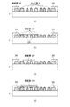
【解決手段】配線基板6は、フレキシブル基板1の表面にアディティブ法により高密度な配線層2Aを有する。そして、配線層2Aに重ねて形成される配線層2Bの領域に対して、配線層2Aを覆うように絶縁層3Bを形成する。次に、絶縁層3Bに重ねて配線層2Bを形成し、配線層2Bにさらに重ねて絶縁層3Cと配線層2Cとを形成する。配線層2B,2Cは、インクジェット法にて形成されている。
【選択図】 図2
Description
(実施形態1)
(実施形態2)
(実施形態3)
Claims (15)
- 基板の表面にフォトリソグラフィーにより形成されている第一の配線層と、
前記第一の配線層に重ねて形成されるべき第二の配線層の領域に対して前記第一の配線層を覆うようにインクジェット法により形成されている第一の絶縁層と、
前記第一の絶縁層に重ねてインクジェット法により形成されている第二の配線層とを有することを特徴とする配線基板。 - 請求項1に記載の配線基板において、
前記第二の配線層にさらに重ねて絶縁層と配線層とが順にインクジェット法により繰り返し形成されていることを特徴とする配線基板。 - 請求項1または2に記載の配線基板において、
前記配線層は前記絶縁層に覆われない露出部を有することを特徴とする配線基板。 - 請求項3に記載の配線基板において、
重ねて形成されている前記配線層が前記露出部で接続され電気的に導通していることを特徴とする配線基板。 - 請求項3または4に記載の配線基板において、
前記配線層の前記露出部分に電子部品が装着されていることを特徴とする配線基板。 - 請求項1から5のいずれか一項に記載の配線基板を搭載していることを特徴とする電気光学装置。
- 請求項6に記載の電気光学装置を搭載していることを特徴とする電子機器。
- 基板の表面にフォトリソグラフィーにより第一の配線層を形成する工程と、
前記第一の配線層に重ねて前記第一の配線層の露出部を接続するために形成されるべき第二の配線層の領域に対して前記露出部を除いた部分を覆うようにインクジェット法により第一の絶縁層を形成する工程と、
前記第一の絶縁層に重ねて第二の配線層をインクジェット法により形成する工程とを有することを特徴とする配線基板の製造方法。 - 請求項8に記載の配線基板の製造方法において、
前記第二の配線層にさらに重ねて絶縁層と配線層とを順にインクジェット法により繰り返し形成する工程を有することを特徴とする配線基板の製造方法。 - 基板の表面にフォトリソグラフィーにより第一の配線層を形成する工程と、
前記第一の配線層と面一になるように一段目の絶縁層をインクジェット法により形成する工程と、
前記第一の配線層に重ねて前記第一の配線層の露出部を接続するために形成されるべき第二の配線層の領域に対して前記露出部間に前記第一の配線層および前記一段目の絶縁層を覆うように二段目の絶縁層をインクジェット法により形成する工程と、
前記二段目の絶縁層に重ねて第二の配線層をインクジェット法により形成する工程とを有することを特徴とする配線基板の製造方法。 - 請求項10に記載の配線基板の製造方法において、
前記第二の配線層にさらに重ねて絶縁層と配線層とを順にインクジェット法により繰り返し形成する工程を有することを特徴とする配線基板の製造方法。 - 請求項8から11のいずれか一項に記載の配線基板の製造方法において、
前記配線層を形成する工程では、重ねて形成されている前記配線層が前記露出部で接続され電気的に導通するように形成されていることを特徴とする配線基板の製造方法。 - 請求項12に記載の配線基板の製造方法において、
前記配線層の前記露出部分に電子部品を装着する工程を有することを特徴とする配線基板の製造方法。 - 請求項8から13のいずれか一項に記載の配線基板の製造方法によって製造された配線基板を搭載していることを特徴とする電気光学装置。
- 請求項14に記載の電気光学装置を搭載していることを特徴とする電子機器。
Priority Applications (6)
| Application Number | Priority Date | Filing Date | Title |
|---|---|---|---|
| JP2004201882A JP2006024768A (ja) | 2004-07-08 | 2004-07-08 | 配線基板、配線基板の製造方法および電子機器 |
| TW094119670A TWI277459B (en) | 2004-07-08 | 2005-06-14 | Wiring board, manufacturing method thereof, and electronic appliance |
| US11/156,586 US20060005994A1 (en) | 2004-07-08 | 2005-06-21 | Wiring board, method of manufacturing wiring board, and electronic device |
| CNA2005100810372A CN1719966A (zh) | 2004-07-08 | 2005-06-28 | 布线基板、布线基板的制造方法以及电子机器 |
| KR1020050061490A KR100633669B1 (ko) | 2004-07-08 | 2005-07-08 | 배선 기판 및 그 제조 방법, 전기 광학 장치 및 전자 기기 |
| US12/016,826 US7676913B2 (en) | 2004-07-08 | 2008-01-18 | Wiring board, method of manufacturing wiring board, and electronic device |
Applications Claiming Priority (1)
| Application Number | Priority Date | Filing Date | Title |
|---|---|---|---|
| JP2004201882A JP2006024768A (ja) | 2004-07-08 | 2004-07-08 | 配線基板、配線基板の製造方法および電子機器 |
Publications (1)
| Publication Number | Publication Date |
|---|---|
| JP2006024768A true JP2006024768A (ja) | 2006-01-26 |
Family
ID=35540131
Family Applications (1)
| Application Number | Title | Priority Date | Filing Date |
|---|---|---|---|
| JP2004201882A Pending JP2006024768A (ja) | 2004-07-08 | 2004-07-08 | 配線基板、配線基板の製造方法および電子機器 |
Country Status (5)
| Country | Link |
|---|---|
| US (2) | US20060005994A1 (ja) |
| JP (1) | JP2006024768A (ja) |
| KR (1) | KR100633669B1 (ja) |
| CN (1) | CN1719966A (ja) |
| TW (1) | TWI277459B (ja) |
Cited By (7)
| Publication number | Priority date | Publication date | Assignee | Title |
|---|---|---|---|---|
| JP2012134502A (ja) * | 2010-12-21 | 2012-07-12 | Samsung Electro-Mechanics Co Ltd | 多層印刷回路基板及びその製造方法 |
| CN105057667A (zh) * | 2015-09-02 | 2015-11-18 | 华中科技大学 | 一种3d打印机构 |
| WO2016072011A1 (ja) * | 2014-11-07 | 2016-05-12 | 富士機械製造株式会社 | 配線形成方法 |
| JP2017516295A (ja) * | 2014-03-25 | 2017-06-15 | ストラタシス リミテッド | 層交差パターンを製作する方法及びシステム |
| JP2021168339A (ja) * | 2020-04-10 | 2021-10-21 | 矢崎総業株式会社 | 多層プリント配線板の製造方法 |
| US11191167B2 (en) | 2015-03-25 | 2021-11-30 | Stratasys Ltd. | Method and system for in situ sintering of conductive ink |
| WO2023209960A1 (ja) * | 2022-04-28 | 2023-11-02 | 株式会社Fuji | 設計方法、設計プログラム、および回路基板作製方法 |
Families Citing this family (7)
| Publication number | Priority date | Publication date | Assignee | Title |
|---|---|---|---|---|
| US20070281091A1 (en) * | 2006-05-31 | 2007-12-06 | Cabot Corporation | Polyimide insulative layers in multi-layered printed electronic features |
| KR100768234B1 (ko) * | 2006-06-07 | 2007-10-17 | 삼성에스디아이 주식회사 | 유기 발광 디스플레이 장치 |
| KR100819876B1 (ko) | 2006-09-19 | 2008-04-07 | 삼성전기주식회사 | 합금배선기판 및 그 제조방법 |
| KR101281163B1 (ko) * | 2006-11-21 | 2013-07-02 | 삼성디스플레이 주식회사 | 와이어 그리드 편광자 제조방법 |
| JP2008238531A (ja) * | 2007-03-27 | 2008-10-09 | Brother Ind Ltd | 画像形成装置 |
| CN103763854A (zh) * | 2014-01-18 | 2014-04-30 | 上海美维电子有限公司 | 印刷线路板及其制造方法 |
| US11721858B2 (en) | 2020-12-11 | 2023-08-08 | Kesavan Moses Srivilliputhur | SuCCoR: a super critical cooling regulator to mitigate heating of batteries and other devices |
Family Cites Families (17)
| Publication number | Priority date | Publication date | Assignee | Title |
|---|---|---|---|---|
| FR2560281B1 (fr) * | 1984-02-24 | 1986-09-19 | Nord Mediterranee Chantiers | Installation pour l'extraction de minerais des fonds marins |
| US6378199B1 (en) * | 1994-05-13 | 2002-04-30 | Dai Nippon Printing Co., Ltd. | Multi-layer printed-wiring board process for producing |
| JPH0923063A (ja) | 1995-07-07 | 1997-01-21 | Hitachi Ltd | 多層配線回路基板の製造方法 |
| JPH11163499A (ja) | 1997-11-28 | 1999-06-18 | Nitto Boseki Co Ltd | プリント配線板の製造方法及びこの製造方法によるプリント配線板 |
| JP3980801B2 (ja) * | 1999-09-16 | 2007-09-26 | 株式会社東芝 | 三次元構造体およびその製造方法 |
| JP2002162652A (ja) * | 2000-01-31 | 2002-06-07 | Fujitsu Ltd | シート状表示装置、樹脂球状体、及びマイクロカプセル |
| US6887650B2 (en) * | 2001-07-24 | 2005-05-03 | Seiko Epson Corporation | Transfer method, method of manufacturing thin film devices, method of manufacturing integrated circuits, circuit board and manufacturing method thereof, electro-optical apparatus and manufacturing method thereof, ic card, and electronic appliance |
| JP2003037363A (ja) | 2001-07-25 | 2003-02-07 | Denso Corp | 多層基板用素板の製造方法、その製造方法により製造された多層基板用素板を用いた多層基板の製造方法および多層基板用素板 |
| CN1222918C (zh) * | 2001-08-27 | 2005-10-12 | 佳能株式会社 | 布线基板及使用该布线基板的图象显示装置 |
| JP4125153B2 (ja) * | 2002-02-20 | 2008-07-30 | キヤノン株式会社 | 半導体装置及びそれを用いた液体吐出装置 |
| JP4572501B2 (ja) | 2002-02-27 | 2010-11-04 | コニカミノルタホールディングス株式会社 | 有機薄膜トランジスタの製造方法 |
| JP4272854B2 (ja) * | 2002-07-10 | 2009-06-03 | キヤノン株式会社 | 半導体装置及びそれを用いた液体吐出装置 |
| US7138157B2 (en) * | 2002-07-30 | 2006-11-21 | Canon Kabushiki Kaisha | Electron emitting device manufacture method and image display apparatus manufacture method |
| JP3801158B2 (ja) | 2002-11-19 | 2006-07-26 | セイコーエプソン株式会社 | 多層配線基板の製造方法、多層配線基板、電子デバイス及び電子機器 |
| JP3900125B2 (ja) * | 2002-11-26 | 2007-04-04 | セイコーエプソン株式会社 | 有機エレクトロルミネッセンス装置の製造方法 |
| US20050006339A1 (en) * | 2003-07-11 | 2005-01-13 | Peter Mardilovich | Electroless deposition methods and systems |
| JP3690407B2 (ja) * | 2003-07-31 | 2005-08-31 | セイコーエプソン株式会社 | 半導体装置の製造方法 |
-
2004
- 2004-07-08 JP JP2004201882A patent/JP2006024768A/ja active Pending
-
2005
- 2005-06-14 TW TW094119670A patent/TWI277459B/zh not_active IP Right Cessation
- 2005-06-21 US US11/156,586 patent/US20060005994A1/en not_active Abandoned
- 2005-06-28 CN CNA2005100810372A patent/CN1719966A/zh active Pending
- 2005-07-08 KR KR1020050061490A patent/KR100633669B1/ko not_active Expired - Fee Related
-
2008
- 2008-01-18 US US12/016,826 patent/US7676913B2/en not_active Expired - Lifetime
Cited By (10)
| Publication number | Priority date | Publication date | Assignee | Title |
|---|---|---|---|---|
| JP2012134502A (ja) * | 2010-12-21 | 2012-07-12 | Samsung Electro-Mechanics Co Ltd | 多層印刷回路基板及びその製造方法 |
| JP2017516295A (ja) * | 2014-03-25 | 2017-06-15 | ストラタシス リミテッド | 層交差パターンを製作する方法及びシステム |
| JP2019196019A (ja) * | 2014-03-25 | 2019-11-14 | ストラタシス リミテッド | 層交差パターンを製作する方法及びシステム |
| US11090858B2 (en) | 2014-03-25 | 2021-08-17 | Stratasys Ltd. | Method and system for fabricating cross-layer pattern |
| US11904525B2 (en) | 2014-03-25 | 2024-02-20 | Stratasys Ltd. | Method and system for fabricating cross-layer pattern |
| WO2016072011A1 (ja) * | 2014-11-07 | 2016-05-12 | 富士機械製造株式会社 | 配線形成方法 |
| US11191167B2 (en) | 2015-03-25 | 2021-11-30 | Stratasys Ltd. | Method and system for in situ sintering of conductive ink |
| CN105057667A (zh) * | 2015-09-02 | 2015-11-18 | 华中科技大学 | 一种3d打印机构 |
| JP2021168339A (ja) * | 2020-04-10 | 2021-10-21 | 矢崎総業株式会社 | 多層プリント配線板の製造方法 |
| WO2023209960A1 (ja) * | 2022-04-28 | 2023-11-02 | 株式会社Fuji | 設計方法、設計プログラム、および回路基板作製方法 |
Also Published As
| Publication number | Publication date |
|---|---|
| TWI277459B (en) | 2007-04-01 |
| TW200605967A (en) | 2006-02-16 |
| CN1719966A (zh) | 2006-01-11 |
| KR100633669B1 (ko) | 2006-10-11 |
| US7676913B2 (en) | 2010-03-16 |
| US20080115351A1 (en) | 2008-05-22 |
| KR20060049955A (ko) | 2006-05-19 |
| US20060005994A1 (en) | 2006-01-12 |
Similar Documents
| Publication | Publication Date | Title |
|---|---|---|
| US7676913B2 (en) | Wiring board, method of manufacturing wiring board, and electronic device | |
| JP4100385B2 (ja) | 多層構造形成方法、配線基板の製造方法、および電子機器の製造方法 | |
| JP4059260B2 (ja) | 多層構造形成方法、配線基板の製造方法、および電子機器の製造方法 | |
| KR101389363B1 (ko) | 액적 토출 헤드, 액적 토출 헤드의 제조 방법, 및 액적토출 장치 | |
| JP2003311197A (ja) | 製膜方法と液滴吐出ヘッド、液滴吐出装置及びデバイスの製造方法、デバイス並びに電子機器 | |
| US7784913B2 (en) | Mounted structure, liquid droplet ejection head, liquid droplet ejection apparatus and manufacturing method | |
| JP2009202473A (ja) | インクジェットヘッドの製造方法およびインクジェットヘッド | |
| US9186892B2 (en) | Liquid jet head and liquid jet apparatus | |
| JP2001080074A (ja) | インクジェットプリンタ用プリントヘッド | |
| JP4096962B2 (ja) | 多層構造形成方法、配線基板および電子機器の製造方法 | |
| JP2007021760A (ja) | 薄膜形成装置 | |
| JP2006073561A (ja) | 回路基板 | |
| JP2008034880A (ja) | 多層構造形成方法、配線基板および電子機器の製造方法 | |
| JP2006019567A (ja) | シールド線 | |
| JP2005317744A (ja) | 金属配線の製造方法、電気光学装置、および電子機器 | |
| JP2006305987A (ja) | 液滴吐出ヘッド、及び液滴吐出ヘッドの製造方法 | |
| JP4193758B2 (ja) | 層形成装置 | |
| JP2005327985A (ja) | 電極間接続構造、電極間接続方法、及び電子機器 | |
| CN108248220A (zh) | 液体喷射头、以及液体喷射记录装置 | |
| JP2011204748A (ja) | 配線パターン形成方法、及び配線基板 | |
| JP4826782B2 (ja) | パターン形成装置 | |
| JP2010082577A (ja) | パターン膜形成部材、パターン膜形成部材の製造方法、電気光学装置、電子機器 | |
| JP4888072B2 (ja) | 電子基板の製造方法 | |
| JP2008029978A (ja) | 描画装置、液状体の描画方法、配線基板の製造方法 | |
| JP2006147649A (ja) | 電子デバイス装置の製造方法、電子デバイス装置及び電子機器 |
Legal Events
| Date | Code | Title | Description |
|---|---|---|---|
| A977 | Report on retrieval |
Free format text: JAPANESE INTERMEDIATE CODE: A971007 Effective date: 20070403 |
|
| RD04 | Notification of resignation of power of attorney |
Free format text: JAPANESE INTERMEDIATE CODE: A7424 Effective date: 20070403 |
|
| A131 | Notification of reasons for refusal |
Free format text: JAPANESE INTERMEDIATE CODE: A131 Effective date: 20070424 |
|
| A521 | Request for written amendment filed |
Free format text: JAPANESE INTERMEDIATE CODE: A523 Effective date: 20070528 |
|
| A02 | Decision of refusal |
Free format text: JAPANESE INTERMEDIATE CODE: A02 Effective date: 20071016 |