JP2006165332A - 半導体記憶装置 - Google Patents
半導体記憶装置 Download PDFInfo
- Publication number
- JP2006165332A JP2006165332A JP2004355720A JP2004355720A JP2006165332A JP 2006165332 A JP2006165332 A JP 2006165332A JP 2004355720 A JP2004355720 A JP 2004355720A JP 2004355720 A JP2004355720 A JP 2004355720A JP 2006165332 A JP2006165332 A JP 2006165332A
- Authority
- JP
- Japan
- Prior art keywords
- fuse element
- transistor
- node
- memory device
- semiconductor memory
- Prior art date
- Legal status (The legal status is an assumption and is not a legal conclusion. Google has not performed a legal analysis and makes no representation as to the accuracy of the status listed.)
- Granted
Links
Images




Classifications
-
- H—ELECTRICITY
- H10—SEMICONDUCTOR DEVICES; ELECTRIC SOLID-STATE DEVICES NOT OTHERWISE PROVIDED FOR
- H10W—GENERIC PACKAGES, INTERCONNECTIONS, CONNECTORS OR OTHER CONSTRUCTIONAL DETAILS OF DEVICES COVERED BY CLASS H10
- H10W20/00—Interconnections in chips, wafers or substrates
- H10W20/40—Interconnections external to wafers or substrates, e.g. back-end-of-line [BEOL] metallisations or vias connecting to gate electrodes
- H10W20/49—Adaptable interconnections, e.g. fuses or antifuses
- H10W20/493—Fuses, i.e. interconnections changeable from conductive to non-conductive
- H10W20/494—Fuses, i.e. interconnections changeable from conductive to non-conductive changeable by the use of an external beam, e.g. laser beam or ion beam
-
- G—PHYSICS
- G11—INFORMATION STORAGE
- G11C—STATIC STORES
- G11C17/00—Read-only memories programmable only once; Semi-permanent stores, e.g. manually-replaceable information cards
- G11C17/14—Read-only memories programmable only once; Semi-permanent stores, e.g. manually-replaceable information cards in which contents are determined by selectively establishing, breaking or modifying connecting links by permanently altering the state of coupling elements, e.g. PROM
- G11C17/16—Read-only memories programmable only once; Semi-permanent stores, e.g. manually-replaceable information cards in which contents are determined by selectively establishing, breaking or modifying connecting links by permanently altering the state of coupling elements, e.g. PROM using electrically-fusible links
-
- G—PHYSICS
- G11—INFORMATION STORAGE
- G11C—STATIC STORES
- G11C17/00—Read-only memories programmable only once; Semi-permanent stores, e.g. manually-replaceable information cards
- G11C17/14—Read-only memories programmable only once; Semi-permanent stores, e.g. manually-replaceable information cards in which contents are determined by selectively establishing, breaking or modifying connecting links by permanently altering the state of coupling elements, e.g. PROM
- G11C17/18—Auxiliary circuits, e.g. for writing into memory
Landscapes
- Design And Manufacture Of Integrated Circuits (AREA)
- Semiconductor Integrated Circuits (AREA)
- Semiconductor Memories (AREA)
Abstract
【解決手段】半導体記憶装置は、第1及び第2端子を有し、且つ前記第1端子と前記第2端子との間がレーザーにより電気的に切断されたか否かにより情報を記憶するフューズ素子1と、前記フューズ素子の情報が転送されるノードと、前記フューズ素子1と前記ノードとの間に設けられ、且つ前記フューズ素子1の情報を前記ノードにセットするN型トランジスタ2と、前記第1端子に接続されたアノードとカソードとを含み、且つ前記フューズ素子1が前記レーザーにより切断される際に発生する電荷を逃がすダイオード9とを含む。
【選択図】 図1
Description
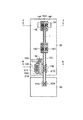
図1は、本発明の第1の実施形態に係る半導体記憶装置の構成を示す回路図である。PチャネルMOSトランジスタ3のゲートには、プリチャージ信号PRCが入力されている。トランジスタ3のソースは、電源電圧VDDに接続されている。トランジスタ3のドレインは、ノードSに接続されている。
第2の実施形態は、フューズ素子1に接続されたPチャネルMOSトランジスタが破壊されるのを防止するように半導体記憶装置を構成したものである。
第3の実施形態は、フューズ素子1とトランジスタとの間に拡散層で形成された抵抗を接続することで、レーザー照射時にトランジスタが破壊されるのを防止するようにしたものである。
第4の実施形態は、フューズ素子1とNチャネルMOSトランジスタ2との間に、配線抵抗と配線容量とを付加することで、NチャネルMOSトランジスタ2を保護するようにしたものである。
第5の実施形態は、フューズ素子1とトランジスタの拡散層とを接続するコンタクトプラグと、トランジスタのゲートとの距離を離すことでゲート絶縁膜を保護するようにしたものである。
(2)コンタクトプラグ65,67の径の1.5倍以上
(3)ゲート長の4倍以上
(4)実効ゲート酸化膜厚の100倍以上
このようにトランジスタ60を形成することで、フューズ素子1にレーザーを照射する際に発生する電荷により誘起される電界が、ゲート絶縁膜61に集中するのを緩和することができる。これにより、ゲート絶縁膜61が破壊されるのを防止することができる。
第6の実施形態は、フューズ素子1に接続されるNチャネルMOSトランジスタ70のゲート絶縁膜を厚くすることで、フューズ素子1にレーザーを照射する際に発生する電荷によりゲート絶縁膜が破壊されるのを防止するようにしたものである。
Claims (5)
- 第1及び第2端子を有し、且つ前記第1端子と前記第2端子との間がレーザーにより電気的に切断されたか否かにより情報を記憶するフューズ素子と、
前記フューズ素子の情報が転送されるノードと、
前記フューズ素子と前記ノードとの間に設けられ、且つ前記フューズ素子の情報を前記ノードにセットするN型トランジスタと、
前記第1端子に接続されたアノードとカソードとを含み、且つ前記フューズ素子が前記レーザーにより切断される際に発生する電荷を逃がすダイオードと
を具備することを特徴とする半導体記憶装置。 - 前記フューズ素子、前記N型トランジスタ及び前記ダイオードが設けられる基板をさらに具備し、
前記ダイオードは、前記基板に設けられたN型半導体領域と、前記第1端子に接続され且つ前記N型半導体領域に設けられたP型拡散層とを含むことを特徴とする請求項1記載の半導体記憶装置。 - 基板と、
前記基板に設けられ、且つ第1及び第2端子を有し、且つ前記第1端子と前記第2端子との間がレーザーにより電気的に切断されたか否かにより情報を記憶するフューズ素子と、
前記基板に設けられ、且つ前記第1端子に接続された第1導電型半導体領域と、
前記フューズ素子の情報が転送されるノードと、
前記基板に設けられ、且つ前記第1導電型半導体領域と前記ノードとの間に設けられ、且つ前記フューズ素子の情報を前記ノードにセットするトランジスタと
を具備することを特徴とする半導体記憶装置。 - 前記基板に設けられた第2導電型半導体領域をさらに具備し、
前記第1導電型半導体領域と前記トランジスタとは、前記第2導電型半導体領域に設けられることを特徴とする請求項3記載の半導体記憶装置。 - 第1及び第2端子を有し、且つ前記第1端子と前記第2端子との間がレーザーにより電気的に切断されたか否かにより情報を記憶するフューズ素子と、
抵抗値を有し、且つ前記第1端子に接続された第1配線部と、
前記フューズ素子の情報が転送されるノードと、
前記第1配線部と前記ノードとの間に設けられ、且つ前記フューズ素子の情報を前記ノードにセットするトランジスタと
を具備することを特徴とする半導体記憶装置。
Priority Applications (3)
| Application Number | Priority Date | Filing Date | Title |
|---|---|---|---|
| JP2004355720A JP4901096B2 (ja) | 2004-12-08 | 2004-12-08 | 半導体記憶装置 |
| US11/293,378 US7218560B2 (en) | 2004-12-08 | 2005-12-05 | Semiconductor memory device |
| CNA2005101294041A CN1815630A (zh) | 2004-12-08 | 2005-12-07 | 半导体存储器 |
Applications Claiming Priority (1)
| Application Number | Priority Date | Filing Date | Title |
|---|---|---|---|
| JP2004355720A JP4901096B2 (ja) | 2004-12-08 | 2004-12-08 | 半導体記憶装置 |
Publications (2)
| Publication Number | Publication Date |
|---|---|
| JP2006165332A true JP2006165332A (ja) | 2006-06-22 |
| JP4901096B2 JP4901096B2 (ja) | 2012-03-21 |
Family
ID=36573527
Family Applications (1)
| Application Number | Title | Priority Date | Filing Date |
|---|---|---|---|
| JP2004355720A Expired - Fee Related JP4901096B2 (ja) | 2004-12-08 | 2004-12-08 | 半導体記憶装置 |
Country Status (3)
| Country | Link |
|---|---|
| US (1) | US7218560B2 (ja) |
| JP (1) | JP4901096B2 (ja) |
| CN (1) | CN1815630A (ja) |
Cited By (1)
| Publication number | Priority date | Publication date | Assignee | Title |
|---|---|---|---|---|
| KR100827664B1 (ko) | 2006-12-26 | 2008-05-07 | 삼성전자주식회사 | 전기적인 퓨즈, 이를 갖는 반도체 소자, 및 전기적인퓨즈의 프로그래밍과 리딩 방법 |
Families Citing this family (5)
| Publication number | Priority date | Publication date | Assignee | Title |
|---|---|---|---|---|
| DE102006001729A1 (de) * | 2006-01-13 | 2007-07-19 | Robert Bosch Gmbh | Baugruppe mit mechanisch unzugänglicher oder schwer zugänglicher Schaltung sowie Verfahren zur Umschaltung des Betriebszustandes einer Baugruppe |
| EP2020684A3 (en) * | 2007-07-25 | 2009-04-08 | NEC Electronics Corporation | Semiconductor device and offset voltage adjusting method |
| US7567115B2 (en) * | 2007-11-01 | 2009-07-28 | Elite Semiconductor Memory Technology Inc. | Fuse-fetching circuit and method for using the same |
| CN112397544B (zh) * | 2020-11-12 | 2021-09-14 | 长江先进存储产业创新中心有限责任公司 | 一种三维相变存储器及其控制方法 |
| NL2034620B1 (en) * | 2023-04-18 | 2024-10-28 | Sandgrain B V | Integrated circuit with hard-coded ic-specific code |
Citations (4)
| Publication number | Priority date | Publication date | Assignee | Title |
|---|---|---|---|---|
| JPH10321806A (ja) * | 1997-05-23 | 1998-12-04 | Sony Corp | 半導体装置の保護回路 |
| JPH11251530A (ja) * | 1998-03-04 | 1999-09-17 | Fujitsu Ltd | 半導体装置 |
| JP2002033393A (ja) * | 1991-06-27 | 2002-01-31 | Hitachi Ltd | 半導体集積回路装置およびその製造方法 |
| JP2003007836A (ja) * | 2001-06-26 | 2003-01-10 | Toshiba Corp | 半導体チップ及び半導体モジュール |
Family Cites Families (6)
| Publication number | Priority date | Publication date | Assignee | Title |
|---|---|---|---|---|
| US5457656A (en) * | 1994-08-17 | 1995-10-10 | United Microelectronics Corp. | Zero static power memory device redundancy circuitry |
| JP3786527B2 (ja) * | 1998-10-06 | 2006-06-14 | 富士通株式会社 | 半導体装置及び半導体チップ上レイアウト設計方法 |
| US6525350B1 (en) * | 1999-07-16 | 2003-02-25 | Kawasaki Steel Corporation | Semiconductor integrated circuit basic cell semiconductor integrated circuit using the same |
| JP2001266589A (ja) * | 2000-03-21 | 2001-09-28 | Toshiba Corp | 半導体記憶装置およびそのテスト方法 |
| US6762918B2 (en) * | 2002-05-20 | 2004-07-13 | International Business Machines Corporation | Fault free fuse network |
| US6710640B1 (en) | 2002-09-19 | 2004-03-23 | Infineon Technologies Ag | Active well-bias transistor for programming a fuse |
-
2004
- 2004-12-08 JP JP2004355720A patent/JP4901096B2/ja not_active Expired - Fee Related
-
2005
- 2005-12-05 US US11/293,378 patent/US7218560B2/en not_active Expired - Fee Related
- 2005-12-07 CN CNA2005101294041A patent/CN1815630A/zh active Pending
Patent Citations (4)
| Publication number | Priority date | Publication date | Assignee | Title |
|---|---|---|---|---|
| JP2002033393A (ja) * | 1991-06-27 | 2002-01-31 | Hitachi Ltd | 半導体集積回路装置およびその製造方法 |
| JPH10321806A (ja) * | 1997-05-23 | 1998-12-04 | Sony Corp | 半導体装置の保護回路 |
| JPH11251530A (ja) * | 1998-03-04 | 1999-09-17 | Fujitsu Ltd | 半導体装置 |
| JP2003007836A (ja) * | 2001-06-26 | 2003-01-10 | Toshiba Corp | 半導体チップ及び半導体モジュール |
Cited By (2)
| Publication number | Priority date | Publication date | Assignee | Title |
|---|---|---|---|---|
| KR100827664B1 (ko) | 2006-12-26 | 2008-05-07 | 삼성전자주식회사 | 전기적인 퓨즈, 이를 갖는 반도체 소자, 및 전기적인퓨즈의 프로그래밍과 리딩 방법 |
| US7791164B2 (en) | 2006-12-26 | 2010-09-07 | Samsung Electronics Co., Ltd. | Electrical fuse, semiconductor device having the same, and method of programming and reading the electrical fuse |
Also Published As
| Publication number | Publication date |
|---|---|
| CN1815630A (zh) | 2006-08-09 |
| US20060119415A1 (en) | 2006-06-08 |
| JP4901096B2 (ja) | 2012-03-21 |
| US7218560B2 (en) | 2007-05-15 |
Similar Documents
| Publication | Publication Date | Title |
|---|---|---|
| JP3662351B2 (ja) | 半導体装置のヒューズ素子 | |
| JP4981661B2 (ja) | 分割チャネルアンチヒューズアレイ構造 | |
| US8254198B2 (en) | Anti-fuse element | |
| US7272067B1 (en) | Electrically-programmable integrated circuit antifuses | |
| US6657243B2 (en) | Semiconductor device with SRAM section including a plurality of memory cells | |
| US20080316852A1 (en) | Nonvolatile semiconductor memory device | |
| KR20130012565A (ko) | 반도체 집적 회로 | |
| KR102106664B1 (ko) | Otp 셀 및 이를 이용한 otp 메모리 어레이 | |
| CN113963738B (zh) | 反熔丝装置及反熔丝单元的编程方法 | |
| US8625377B2 (en) | Low voltage efuse programming circuit and method | |
| US8928056B2 (en) | Nonvolatile semiconductor memory device | |
| KR100346991B1 (ko) | 반도체 기억 장치 | |
| KR20200057658A (ko) | 안티 퓨즈 메모리 셀 | |
| JP4901096B2 (ja) | 半導体記憶装置 | |
| US20050073024A1 (en) | Integrated semiconductor circuit with an electrically programmable switching element | |
| JP5586819B2 (ja) | 半導体装置 | |
| JP5002967B2 (ja) | 半導体装置及びその製造方法 | |
| US8467240B1 (en) | Integrated circuits with nonvolatile memory elements | |
| JP2974024B2 (ja) | Mosメモリーポイント | |
| CN107967929B (zh) | 一种存储单元及其存储阵列结构、操作方法 | |
| US7362159B2 (en) | Semiconductor integrated circuit | |
| CN108766499B (zh) | E-fuse存储阵列、e-fuse以及e-fuse操作方法 | |
| JP2011044602A (ja) | 不揮発性半導体記憶装置 | |
| US20070181958A1 (en) | Semiconductor device and method of forming the same | |
| JP2008041986A (ja) | 半導体集積回路装置 |
Legal Events
| Date | Code | Title | Description |
|---|---|---|---|
| A621 | Written request for application examination |
Free format text: JAPANESE INTERMEDIATE CODE: A621 Effective date: 20070720 |
|
| A977 | Report on retrieval |
Free format text: JAPANESE INTERMEDIATE CODE: A971007 Effective date: 20100330 |
|
| A131 | Notification of reasons for refusal |
Free format text: JAPANESE INTERMEDIATE CODE: A131 Effective date: 20100406 |
|
| A521 | Request for written amendment filed |
Free format text: JAPANESE INTERMEDIATE CODE: A523 Effective date: 20100527 |
|
| A131 | Notification of reasons for refusal |
Free format text: JAPANESE INTERMEDIATE CODE: A131 Effective date: 20110607 |
|
| A521 | Request for written amendment filed |
Free format text: JAPANESE INTERMEDIATE CODE: A523 Effective date: 20110711 |
|
| TRDD | Decision of grant or rejection written | ||
| A01 | Written decision to grant a patent or to grant a registration (utility model) |
Free format text: JAPANESE INTERMEDIATE CODE: A01 Effective date: 20111206 |
|
| A01 | Written decision to grant a patent or to grant a registration (utility model) |
Free format text: JAPANESE INTERMEDIATE CODE: A01 |
|
| A61 | First payment of annual fees (during grant procedure) |
Free format text: JAPANESE INTERMEDIATE CODE: A61 Effective date: 20111227 |
|
| FPAY | Renewal fee payment (event date is renewal date of database) |
Free format text: PAYMENT UNTIL: 20150113 Year of fee payment: 3 |
|
| LAPS | Cancellation because of no payment of annual fees |