JP4981661B2 - 分割チャネルアンチヒューズアレイ構造 - Google Patents
分割チャネルアンチヒューズアレイ構造 Download PDFInfo
- Publication number
- JP4981661B2 JP4981661B2 JP2007511808A JP2007511808A JP4981661B2 JP 4981661 B2 JP4981661 B2 JP 4981661B2 JP 2007511808 A JP2007511808 A JP 2007511808A JP 2007511808 A JP2007511808 A JP 2007511808A JP 4981661 B2 JP4981661 B2 JP 4981661B2
- Authority
- JP
- Japan
- Prior art keywords
- channel region
- gate
- transistor
- antifuse
- gate oxide
- Prior art date
- Legal status (The legal status is an assumption and is not a legal conclusion. Google has not performed a legal analysis and makes no representation as to the accuracy of the status listed.)
- Expired - Lifetime
Links
Images


Classifications
-
- H—ELECTRICITY
- H10—SEMICONDUCTOR DEVICES; ELECTRIC SOLID-STATE DEVICES NOT OTHERWISE PROVIDED FOR
- H10D—INORGANIC ELECTRIC SEMICONDUCTOR DEVICES
- H10D48/00—Individual devices not covered by groups H10D1/00 - H10D44/00
- H10D48/30—Devices controlled by electric currents or voltages
-
- H—ELECTRICITY
- H10—SEMICONDUCTOR DEVICES; ELECTRIC SOLID-STATE DEVICES NOT OTHERWISE PROVIDED FOR
- H10D—INORGANIC ELECTRIC SEMICONDUCTOR DEVICES
- H10D64/00—Electrodes of devices having potential barriers
- H10D64/01—Manufacture or treatment
- H10D64/013—Manufacture or treatment of electrodes having a conductor capacitively coupled to a semiconductor by an insulator
- H10D64/01302—Manufacture or treatment of electrodes having a conductor capacitively coupled to a semiconductor by an insulator the insulator being formed after the semiconductor body, the semiconductor being silicon
- H10D64/01332—Making the insulator
- H10D64/01336—Making the insulator on single crystalline silicon, e.g. chemical oxidation using a liquid
- H10D64/01346—Making the insulator on single crystalline silicon, e.g. chemical oxidation using a liquid in a gaseous ambient using an oxygen or a water vapour, e.g. oxidation through a layer
-
- G—PHYSICS
- G11—INFORMATION STORAGE
- G11C—STATIC STORES
- G11C17/00—Read-only memories programmable only once; Semi-permanent stores, e.g. manually-replaceable information cards
- G11C17/14—Read-only memories programmable only once; Semi-permanent stores, e.g. manually-replaceable information cards in which contents are determined by selectively establishing, breaking or modifying connecting links by permanently altering the state of coupling elements, e.g. PROM
- G11C17/16—Read-only memories programmable only once; Semi-permanent stores, e.g. manually-replaceable information cards in which contents are determined by selectively establishing, breaking or modifying connecting links by permanently altering the state of coupling elements, e.g. PROM using electrically-fusible links
-
- G—PHYSICS
- G11—INFORMATION STORAGE
- G11C—STATIC STORES
- G11C17/00—Read-only memories programmable only once; Semi-permanent stores, e.g. manually-replaceable information cards
- G11C17/14—Read-only memories programmable only once; Semi-permanent stores, e.g. manually-replaceable information cards in which contents are determined by selectively establishing, breaking or modifying connecting links by permanently altering the state of coupling elements, e.g. PROM
- G11C17/18—Auxiliary circuits, e.g. for writing into memory
-
- H—ELECTRICITY
- H10—SEMICONDUCTOR DEVICES; ELECTRIC SOLID-STATE DEVICES NOT OTHERWISE PROVIDED FOR
- H10B—ELECTRONIC MEMORY DEVICES
- H10B20/00—Read-only memory [ROM] devices
-
- H—ELECTRICITY
- H10—SEMICONDUCTOR DEVICES; ELECTRIC SOLID-STATE DEVICES NOT OTHERWISE PROVIDED FOR
- H10B—ELECTRONIC MEMORY DEVICES
- H10B20/00—Read-only memory [ROM] devices
- H10B20/20—Programmable ROM [PROM] devices comprising field-effect components
- H10B20/25—One-time programmable ROM [OTPROM] devices, e.g. using electrically-fusible links
-
- H—ELECTRICITY
- H10—SEMICONDUCTOR DEVICES; ELECTRIC SOLID-STATE DEVICES NOT OTHERWISE PROVIDED FOR
- H10D—INORGANIC ELECTRIC SEMICONDUCTOR DEVICES
- H10D64/00—Electrodes of devices having potential barriers
- H10D64/20—Electrodes characterised by their shapes, relative sizes or dispositions
- H10D64/27—Electrodes not carrying the current to be rectified, amplified, oscillated or switched, e.g. gates
- H10D64/311—Gate electrodes for field-effect devices
- H10D64/411—Gate electrodes for field-effect devices for FETs
- H10D64/511—Gate electrodes for field-effect devices for FETs for IGFETs
- H10D64/514—Gate electrodes for field-effect devices for FETs for IGFETs characterised by the insulating layers
- H10D64/516—Gate electrodes for field-effect devices for FETs for IGFETs characterised by the insulating layers the thicknesses being non-uniform
-
- H—ELECTRICITY
- H10—SEMICONDUCTOR DEVICES; ELECTRIC SOLID-STATE DEVICES NOT OTHERWISE PROVIDED FOR
- H10D—INORGANIC ELECTRIC SEMICONDUCTOR DEVICES
- H10D64/00—Electrodes of devices having potential barriers
- H10D64/20—Electrodes characterised by their shapes, relative sizes or dispositions
- H10D64/27—Electrodes not carrying the current to be rectified, amplified, oscillated or switched, e.g. gates
- H10D64/311—Gate electrodes for field-effect devices
- H10D64/411—Gate electrodes for field-effect devices for FETs
- H10D64/511—Gate electrodes for field-effect devices for FETs for IGFETs
- H10D64/517—Gate electrodes for field-effect devices for FETs for IGFETs characterised by the conducting layers
- H10D64/519—Gate electrodes for field-effect devices for FETs for IGFETs characterised by the conducting layers characterised by their top-view geometrical layouts
-
- H—ELECTRICITY
- H10—SEMICONDUCTOR DEVICES; ELECTRIC SOLID-STATE DEVICES NOT OTHERWISE PROVIDED FOR
- H10D—INORGANIC ELECTRIC SEMICONDUCTOR DEVICES
- H10D30/00—Field-effect transistors [FET]
- H10D30/60—Insulated-gate field-effect transistors [IGFET]
- H10D30/601—Insulated-gate field-effect transistors [IGFET] having lightly-doped drain or source extensions, e.g. LDD IGFETs or DDD IGFETs
-
- H—ELECTRICITY
- H10—SEMICONDUCTOR DEVICES; ELECTRIC SOLID-STATE DEVICES NOT OTHERWISE PROVIDED FOR
- H10D—INORGANIC ELECTRIC SEMICONDUCTOR DEVICES
- H10D30/00—Field-effect transistors [FET]
- H10D30/60—Insulated-gate field-effect transistors [IGFET]
- H10D30/67—Thin-film transistors [TFT]
- H10D30/6729—Thin-film transistors [TFT] characterised by the electrodes
- H10D30/673—Thin-film transistors [TFT] characterised by the electrodes characterised by the shapes, relative sizes or dispositions of the gate electrodes
-
- H—ELECTRICITY
- H10—SEMICONDUCTOR DEVICES; ELECTRIC SOLID-STATE DEVICES NOT OTHERWISE PROVIDED FOR
- H10W—GENERIC PACKAGES, INTERCONNECTIONS, CONNECTORS OR OTHER CONSTRUCTIONAL DETAILS OF DEVICES COVERED BY CLASS H10
- H10W20/00—Interconnections in chips, wafers or substrates
- H10W20/40—Interconnections external to wafers or substrates, e.g. back-end-of-line [BEOL] metallisations or vias connecting to gate electrodes
- H10W20/49—Adaptable interconnections, e.g. fuses or antifuses
- H10W20/491—Antifuses, i.e. interconnections changeable from non-conductive to conductive
Landscapes
- Semiconductor Memories (AREA)
- Design And Manufacture Of Integrated Circuits (AREA)
Description
標準ゲート酸化膜オーバー基板コンデンサとして形成される。MOSスイッチの場合よりも小であることが求められるアンチヒューズコンデンサの酸化膜絶縁破壊電圧を低減するため、コンデンサ領域内にV字形のグローブが提案された。コンデンサはポリゲートと接地p型基板との間に形成されるので、破壊電圧はアクセストランジスタを介してコンデンサに印加されなければならなかった。アクセストランジスタのゲート/ドレーンエッジ、及びゲート/ソースエッジは、第2フィールド酸化膜に、チャンネル領域のゲート酸化膜よりもかなり厚く配置され、ゲート/S−D絶縁破壊電圧は大きく改善された。

Claims (29)
- 半導体材料上に形成されたアンチヒューズトランジスタであって、
基板内の、チャンネルが所定の長さを有するチャンネル領域上のポリシリコンゲートと、
前記チャンネル領域の第1の端に近接した拡散領域と、
前記チャンネル領域の第2の端に近接した隔離領域と、
前記ポリシリコンゲートと前記基板との間に、前記チャネル領域の第1の端から所定長さの予め決められた場所まで延伸する厚いゲート酸化膜、及び前記予め決められた場所から前記チャネル領域の第2の端まで延伸する薄いゲート酸化膜を有する可変厚さゲート酸化膜と、
前記ポリシリコンゲートと前記拡散領域との間に電流を伝導する前記チャンネル領域の第1の端に近接する破壊抵抗アクセスエッジと、
前記チャンネル領域の第2の端に近接した、前記ポリシリコンゲートと前記チャンネル領域との間に導電性リンクを形成するため可溶性の酸化膜破壊ゾーンとを有するアンチヒューズトランジスタ。 - 前記隔離領域は、前記薄いゲート酸化膜に近接して、フィールド酸化膜領域、浮遊拡散領域、及び前記フィールド酸化膜と浮遊拡散領域とが連結したもののうちの1つを有する、請求項1に記載のアンチヒューズトランジスタ。
- 前記薄いゲート酸化膜は、前記半導体材料上に形成された少なくとも1つの低圧トランジスタゲート酸化膜と同一である、請求項1に記載のアンチヒューズトランジスタ。
- 前記厚いゲート酸化膜は、前記半導体材料上に形成された少なくとも1つの高圧トランジスタゲート酸化膜と同一である、請求項3に記載のアンチヒューズトランジスタ。
- 前記厚いゲート酸化膜部分は、中間ゲート酸化膜と前記薄いゲート酸化膜部分との組合せを含む、請求項4に記載のアンチヒューズトランジスタ。
- 前記浮遊拡散領域、前記チャンネル領域の第2の端、及び前記ポリシリコンゲートのゲートエッジは、互いにある角度をなす少なくとも2本の線分によって決められた共通のエッジを有している、請求項2に記載のアンチヒューズトランジスタ。
- 前記角度は、135度及び90度である、請求項6に記載のアンチヒューズトランジスタ。
- 前記拡散領域は、低圧トランジスタLDDインプラント、高圧トランジスタLDDインプラント、並びに、前記低圧トランジスタ及び高圧トランジスタLDDインプラントの両方を結合したもののうちの1つと同一なLDDインプラントを有する、請求項4に記載のアンチヒューズトランジスタ。
- 前記拡散領域のエッジ及び前記ポリシリコンゲートの一部は、サリサイド化されていない、請求項1に記載のアンチヒューズトランジスタ。
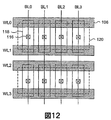
- 行及び列に配置された複数のアンチヒューズトランジスタと、各アンチヒューズトランジスタは、基板内の、チャンネルが所定の長さを有するチャンネル領域上のポリシリコンゲートと、前記チャンネル領域の第1の端に近接した拡散領域と、前記ポリシリコンゲートと前記基板との間に、前記チャネル領域の第1の端から所定長さの予め決められた場所まで延伸する厚いゲート酸化膜、及び前記予め決められた場所から前記チャネル領域の第2の端まで延伸する薄いゲート酸化膜を有する可変厚さゲート酸化膜と、前記チャンネル領域の第2の端に近接した、前記ポリシリコンゲートと前記チャンネル領域との間に導電性リンクを形成するため可溶性の酸化膜破壊ゾーンを有し、
前記アンチヒューズトランジスタの列の拡散領域に連結されたビットラインと、
前記アンチヒューズトランジスタの行の前記ポリシリコンゲートに連結されたワードラインを含むアンチヒューズメモリーアレイ。 - それぞれが前記厚いゲート酸化膜部分に対応したゲート酸化膜を持つトランジスタを有する隔離装置を介して一対の前記ビットラインに連結された感度増幅器をさらに含む、請求項10に記載のアンチヒューズメモリーアレイ。
- 単一エンド(single-ended)の検出操作用の一対の前記ビットラインのうちの1本に連結された1つのアンチヒューズトランジスタに選択的にアクセスし、また、別のアドレス用の一対の前記ビットラインのうちの他の1本に連結されたもう1つのアンチヒューズトランジスタに選択的にアクセスするワードラインデコーディング回路をさらに含む、請求項11に記載のアンチヒューズメモリーアレイ。
- 一対の前記ビットラインのうちの1本に連結された1つのアンチヒューズトランジスタに選択的にアクセスし、また、デュアルエンド(dual-ended)の検出操作用の一対の前記ビットラインのうちの他の1本に連結された1つのアンチヒューズトランジスタに選択的にアクセスするワードラインデコーディング回路をさらに含む、請求項11に記載のアンチヒューズメモリーアレイ。
- 前記ビットラインに連結された列セレクトパスゲートをさらに含み、前記列セレクトパスゲートの少なくとも1つは、前記厚いゲート酸化膜と同一のゲート酸化膜を有する、請求項10に記載のアンチヒューズメモリーアレイ。
- チャネル領域及び拡散領域を有するアンチヒューズトランジスタ用の可変厚さゲート酸化膜を形成する方法であって、
a)前記チャネル領域及び拡散領域を取り囲むフィールド酸化膜を形成する工程、
b)前記チャネル領域に、前記チャネル領域の第1の端から前記チャネル領域の第2の端まで延伸する中間酸化膜を成長させる工程、
c)前記チャネル領域の、前記チャネル領域の前記第1の端から所定長さの予め決められた場所から前記チャネル領域の前記第2の端まで延伸する薄い酸化膜領域から前記中間酸化膜を除去する工程、
d)前記薄い酸化膜領域及び前記中間酸化膜の上に、薄い酸化膜を、前記薄い酸化膜領域の上の前記薄い酸化膜が、それを介して前記チャネル領域まで導電性リンクを形成するため可溶性であるように成長させる工程、
e)前記薄い酸化膜、前記中間酸化膜、及び前記フィールド酸化膜の上にコモンゲートを形成する工程、及び
f)前記中間酸化膜に隣接して前記拡散領域を形成する工程を含む可変厚さゲート酸化膜の形成方法。 - 前記アンチヒューズトランジスタ及び低圧トランジスタは、半導体材料上に形成され、前記低圧トランジスタは、前記薄い酸化膜と同様な絶縁体構造を有する、請求項15に記載の方法。
- 前記拡散領域を形成する工程は、前記薄い酸化膜領域に隣接する浮遊拡散領域を同時に形成することを含む、請求項15に記載の方法。
- 前記中間酸化膜は、前記コモンゲートの第1の端から前記チャネル領域の予め決められた長さまで延伸し、及び前記薄い酸化膜領域上の前記薄いゲート酸化膜は、前記チャネル領域の前記予め決められた長さから前記コモンゲートの第2の端まで延伸する、請求項15に記載の方法。
- 前記予め決められ長さは、マスク工程を介して決定される、請求項18に記載の方法。
- 前記薄い酸化膜は、同じ半導体材料上で低圧トランジスタゲート酸化膜を形成するのと同じプロセス工程で形成される、請求項15に記載の方法。
- 前記薄い酸化膜及び前記中間酸化膜から構成された厚い酸化膜は、同じ半導体材料上で高圧トランジスタゲート酸化膜を形成するのと同じプロセス工程で形成される、請求項15に記載の方法。
- 前記拡散領域の上にサリサイド保護酸化膜を選択的に成長させる工程、及び前記コモンゲート及び前記拡散領域をサリサイド化する工程をさらに含む、請求項15に記載の方法。
- 半導体材料上に形成されたアンチヒューズトランジスタであって、
活性チャネル領域と、
可溶エッジ及びアクセスエッジを区画する前記活性チャネル領域の上に形成されたポリシリコンゲートと、
前記アクセスエッジから前記活性チャネル領域上の所定長さの予め決められた場所まで延伸する厚いゲート酸化膜と、
前記アクセスエッジに隣接した第1の拡散領域と、
前記可溶エッジに隣接した第2の拡散領域と、
前記ポリシリコンゲートと前記活性チャネル領域との間に導電性リンクを形成する前記厚いゲート酸化膜よりも低い破壊電圧を有する、前記活性チャネル領域上の前記予め決められた場所から前記可溶エッジまで延伸する薄いゲート酸化膜とを含むアンチヒューズトランジスタ。 - 前記可溶エッジの長さは、互いにある角度をなす前記ポリシリコンゲートの少なくとも2本の線分によって決定される、請求項23に記載のアンチヒューズトランジスタ。
- 前記可溶エッジの長さは、前記活性チャネル領域の幅よりも大きい、請求項23に記載のアンチヒューズトランジスタ。
- 前記ポリシリコンゲートは、前記可溶エッジと前記アクセスエッジとの間に前記活性チャネル領域を区画し、また、前記厚いゲート酸化膜及び前記薄いゲート酸化膜は、前記チャネル領域と前記ポリシリコンゲートとの間に配置され、前記厚いゲート酸化膜は、前記アクセスエッジから前記活性チャネル領域の予め決められた長さまで延伸し、さらに、前記薄いゲート酸化膜は、前記活性チャネル領域の予め決められた長さから前記可溶エッジまで延伸する、請求項23に記載のアンチヒューズトランジスタ。
- 前記厚いゲート酸化膜は、中間酸化膜と前記薄い酸化膜との組合せである、請求項26に記載のアンチヒューズトランジスタ。
- 前記ポリシリコンゲートは、前記厚いゲート酸化膜の上に配置されるとともに前記活性チャネル領域を区画するための前記拡散領域に隣接して配置された第1部分、前記第1部分のエッジによって区画された前記アクセスエッジ、前記薄いゲート酸化膜の上に配置されるとともに前記第1部分に連結された第2部分、前記第2部分によって区画された前記可溶エッジ、及び前記可溶エッジと前記活性チャネル領域との間に配置された前記第2の拡散領域を有する、請求項23に記載のアンチヒューズトランジスタ。
- 半導体材料上に形成されたアンチヒューズトランジスタであって、
活性チャネル領域と、
可溶エッジ、アクセスエッジ及び隔離エッジを区画する前記活性チャネル領域の上に形成されたポリシリコンゲートと、
前記アクセスエッジから前記活性チャネル領域上の所定長さの予め決められた場所まで延伸する厚いゲート酸化膜と、
前記アクセスエッジに隣接した拡散領域と、
前記隔離エッジに隣接したフィールド酸化膜と、
前記予め決められた場所と前記隔離エッジとの間に、前記ポリシリコンゲートと前記活性チャネル領域との間に導電性リンクを形成する前記厚いゲート酸化膜よりも低い破壊電圧を持った可溶領域を有する薄いゲート酸化膜を含むアンチヒューズトランジスタ。
Applications Claiming Priority (3)
| Application Number | Priority Date | Filing Date | Title |
|---|---|---|---|
| US56831504P | 2004-05-06 | 2004-05-06 | |
| US60/568,315 | 2004-05-06 | ||
| PCT/CA2005/000701 WO2005109516A1 (en) | 2004-05-06 | 2005-05-06 | Split-channel antifuse array architecture |
Publications (2)
| Publication Number | Publication Date |
|---|---|
| JP2007536744A JP2007536744A (ja) | 2007-12-13 |
| JP4981661B2 true JP4981661B2 (ja) | 2012-07-25 |
Family
ID=35320478
Family Applications (1)
| Application Number | Title | Priority Date | Filing Date |
|---|---|---|---|
| JP2007511808A Expired - Lifetime JP4981661B2 (ja) | 2004-05-06 | 2005-05-06 | 分割チャネルアンチヒューズアレイ構造 |
Country Status (7)
| Country | Link |
|---|---|
| US (3) | US7402855B2 (ja) |
| EP (1) | EP1743380B1 (ja) |
| JP (1) | JP4981661B2 (ja) |
| KR (1) | KR101144218B1 (ja) |
| CA (1) | CA2520140C (ja) |
| IL (1) | IL179080A (ja) |
| WO (1) | WO2005109516A1 (ja) |
Families Citing this family (188)
| Publication number | Priority date | Publication date | Assignee | Title |
|---|---|---|---|---|
| US7211418B2 (en) * | 1999-01-14 | 2007-05-01 | Martek Biosciences Corporation | PUFA polyketide synthase systems and uses thereof |
| JP3935139B2 (ja) | 2002-11-29 | 2007-06-20 | 株式会社東芝 | 半導体記憶装置 |
| US9123572B2 (en) | 2004-05-06 | 2015-09-01 | Sidense Corporation | Anti-fuse memory cell |
| US7755162B2 (en) * | 2004-05-06 | 2010-07-13 | Sidense Corp. | Anti-fuse memory cell |
| US8735297B2 (en) | 2004-05-06 | 2014-05-27 | Sidense Corporation | Reverse optical proximity correction method |
| US7511982B2 (en) * | 2004-05-06 | 2009-03-31 | Sidense Corp. | High speed OTP sensing scheme |
| US8767433B2 (en) | 2004-05-06 | 2014-07-01 | Sidense Corp. | Methods for testing unprogrammed OTP memory |
| JP4981661B2 (ja) * | 2004-05-06 | 2012-07-25 | サイデンス コーポレーション | 分割チャネルアンチヒューズアレイ構造 |
| US7190629B2 (en) * | 2005-02-08 | 2007-03-13 | Micron Technology, Inc. | Circuit and method for reading an antifuse |
| US7553704B2 (en) * | 2005-06-28 | 2009-06-30 | Freescale Semiconductor, Inc. | Antifuse element and method of manufacture |
| US7915916B2 (en) * | 2006-06-01 | 2011-03-29 | Micron Technology, Inc. | Antifuse programming circuit with snapback select transistor |
| US8122307B1 (en) * | 2006-08-15 | 2012-02-21 | Synopsys, Inc. | One time programmable memory test structures and methods |
| US7755132B2 (en) * | 2006-08-16 | 2010-07-13 | Sandisk Corporation | Nonvolatile memories with shaped floating gates |
| JP2008090895A (ja) * | 2006-09-29 | 2008-04-17 | Toshiba Corp | 半導体記憶装置 |
| JP5448837B2 (ja) * | 2006-12-22 | 2014-03-19 | シデンス・コーポレーション | マスクプログラム可能なアンチヒューズ構造 |
| US7471540B2 (en) * | 2007-01-24 | 2008-12-30 | Kilopass Technology, Inc. | Non-volatile semiconductor memory based on enhanced gate oxide breakdown |
| US7888200B2 (en) | 2007-01-31 | 2011-02-15 | Sandisk 3D Llc | Embedded memory in a CMOS circuit and methods of forming the same |
| US7868388B2 (en) * | 2007-01-31 | 2011-01-11 | Sandisk 3D Llc | Embedded memory in a CMOS circuit and methods of forming the same |
| US20080296701A1 (en) * | 2007-05-29 | 2008-12-04 | Ememory Technology Inc. | One-time programmable read-only memory |
| FI122011B (fi) * | 2007-06-08 | 2011-07-15 | Teknologian Tutkimuskeskus Vtt | Menetelmä elektroniikkamoduulin tuottamiseksi, välituote elektroniikkamoduulin valmistamiseksi, muistielementti, painettu elektroniikkatuote, anturilaite sekä RFID-tunniste |
| US20090039462A1 (en) * | 2007-08-07 | 2009-02-12 | Mediatek Inc. | Efuse devices and efuse arrays thereof and efuse blowing methods |
| US8058701B2 (en) * | 2007-10-16 | 2011-11-15 | Samsung Electronics Co., Ltd. | Antifuse structures, antifuse array structures, methods of manufacturing the same |
| JP2009147003A (ja) * | 2007-12-12 | 2009-07-02 | Toshiba Corp | 半導体記憶装置 |
| JP5537020B2 (ja) * | 2008-01-18 | 2014-07-02 | ルネサスエレクトロニクス株式会社 | 不揮発性半導体記憶装置 |
| JP2009206490A (ja) * | 2008-01-30 | 2009-09-10 | Elpida Memory Inc | 半導体装置及びその製造方法 |
| KR101051673B1 (ko) | 2008-02-20 | 2011-07-26 | 매그나칩 반도체 유한회사 | 안티퓨즈 및 그 형성방법, 이를 구비한 비휘발성 메모리소자의 단위 셀 |
| US8526254B2 (en) | 2008-04-03 | 2013-09-03 | Sidense Corp. | Test cells for an unprogrammed OTP memory array |
| US8059479B2 (en) * | 2008-04-03 | 2011-11-15 | Sidense Corp. | Test circuit for an unprogrammed OTP memory array |
| US8933492B2 (en) * | 2008-04-04 | 2015-01-13 | Sidense Corp. | Low VT antifuse device |
| US20090309139A1 (en) * | 2008-06-13 | 2009-12-17 | International Business Machines Corporation | Asymmetric gate electrode and method of manufacture |
| US7825479B2 (en) * | 2008-08-06 | 2010-11-02 | International Business Machines Corporation | Electrical antifuse having a multi-thickness dielectric layer |
| JP5563577B2 (ja) * | 2008-09-11 | 2014-07-30 | イートレックス・インコーポレーテッド | 双方向インバータ・チャージャ及びインバータ・チャージャ装置 |
| US8101471B2 (en) * | 2008-12-30 | 2012-01-24 | Intel Corporation | Method of forming programmable anti-fuse element |
| CN102308338B (zh) * | 2009-02-06 | 2015-08-05 | 赛鼎矽公司 | 高可靠性的otp存储器 |
| US8049299B2 (en) | 2009-02-25 | 2011-11-01 | Freescale Semiconductor, Inc. | Antifuses with curved breakdown regions |
| US8223526B2 (en) * | 2009-02-27 | 2012-07-17 | Sidense Corp. | Low power antifuse sensing scheme with improved reliability |
| US8138037B2 (en) * | 2009-03-17 | 2012-03-20 | International Business Machines Corporation | Method and structure for gate height scaling with high-k/metal gate technology |
| US8054673B2 (en) | 2009-04-16 | 2011-11-08 | Seagate Technology Llc | Three dimensionally stacked non volatile memory units |
| JP2011100823A (ja) * | 2009-11-05 | 2011-05-19 | Renesas Electronics Corp | 半導体記憶装置及び半導体記憶装置の製造方法 |
| US9378443B2 (en) | 2009-05-14 | 2016-06-28 | Ascensia Diabetes Care Holding Ag | Calibration coded sensors and apparatus, systems and methods for reading same |
| US8203188B2 (en) * | 2009-05-22 | 2012-06-19 | Broadcom Corporation | Split gate oxides for a laterally diffused metal oxide semiconductor (LDMOS) |
| US8638589B2 (en) * | 2009-07-30 | 2014-01-28 | Ememory Technology Inc. | Operating method for non-volatile memory unit |
| US9013910B2 (en) * | 2009-07-30 | 2015-04-21 | Ememory Technology Inc. | Antifuse OTP memory cell with performance improvement prevention and operating method of memory |
| US8208312B1 (en) | 2009-09-22 | 2012-06-26 | Novocell Semiconductor, Inc. | Non-volatile memory element integratable with standard CMOS circuitry |
| US8134859B1 (en) | 2009-09-25 | 2012-03-13 | Novocell Semiconductor, Inc. | Method of sensing a programmable non-volatile memory element |
| US8199590B1 (en) | 2009-09-25 | 2012-06-12 | Novocell Semiconductor, Inc. | Multiple time programmable non-volatile memory element |
| US8471355B2 (en) * | 2009-10-30 | 2013-06-25 | Sidense Corp. | AND-type one time programmable memory cell |
| US9129687B2 (en) | 2009-10-30 | 2015-09-08 | Sidense Corp. | OTP memory cell having low current leakage |
| US8227873B2 (en) * | 2010-04-09 | 2012-07-24 | Broadcom Corporation | Integrated one-time programmable semiconductor device pair |
| US8283722B2 (en) | 2010-06-14 | 2012-10-09 | Broadcom Corporation | Semiconductor device having an enhanced well region |
| KR101338736B1 (ko) * | 2010-07-28 | 2013-12-06 | 매그나칩 반도체 유한회사 | 안티퓨즈 및 그 형성방법, 이를 구비한 비휘발성 메모리 소자의 단위 셀 |
| US9224496B2 (en) * | 2010-08-11 | 2015-12-29 | Shine C. Chung | Circuit and system of aggregated area anti-fuse in CMOS processes |
| US9236141B2 (en) | 2010-08-20 | 2016-01-12 | Shine C. Chung | Circuit and system of using junction diode of MOS as program selector for programmable resistive devices |
| US10916317B2 (en) | 2010-08-20 | 2021-02-09 | Attopsemi Technology Co., Ltd | Programmable resistance memory on thin film transistor technology |
| US9711237B2 (en) | 2010-08-20 | 2017-07-18 | Attopsemi Technology Co., Ltd. | Method and structure for reliable electrical fuse programming |
| US10249379B2 (en) | 2010-08-20 | 2019-04-02 | Attopsemi Technology Co., Ltd | One-time programmable devices having program selector for electrical fuses with extended area |
| US8929122B2 (en) | 2010-08-20 | 2015-01-06 | Shine C. Chung | Circuit and system of using a junction diode as program selector for resistive devices |
| US9019742B2 (en) | 2010-08-20 | 2015-04-28 | Shine C. Chung | Multiple-state one-time programmable (OTP) memory to function as multi-time programmable (MTP) memory |
| US10923204B2 (en) | 2010-08-20 | 2021-02-16 | Attopsemi Technology Co., Ltd | Fully testible OTP memory |
| US9824768B2 (en) | 2015-03-22 | 2017-11-21 | Attopsemi Technology Co., Ltd | Integrated OTP memory for providing MTP memory |
| US8830720B2 (en) * | 2010-08-20 | 2014-09-09 | Shine C. Chung | Circuit and system of using junction diode as program selector and MOS as read selector for one-time programmable devices |
| US9431127B2 (en) | 2010-08-20 | 2016-08-30 | Shine C. Chung | Circuit and system of using junction diode as program selector for metal fuses for one-time programmable devices |
| US9042153B2 (en) | 2010-08-20 | 2015-05-26 | Shine C. Chung | Programmable resistive memory unit with multiple cells to improve yield and reliability |
| US9070437B2 (en) | 2010-08-20 | 2015-06-30 | Shine C. Chung | Circuit and system of using junction diode as program selector for one-time programmable devices with heat sink |
| US9818478B2 (en) | 2012-12-07 | 2017-11-14 | Attopsemi Technology Co., Ltd | Programmable resistive device and memory using diode as selector |
| US9025357B2 (en) | 2010-08-20 | 2015-05-05 | Shine C. Chung | Programmable resistive memory unit with data and reference cells |
| US8488359B2 (en) | 2010-08-20 | 2013-07-16 | Shine C. Chung | Circuit and system of using junction diode as program selector for one-time programmable devices |
| US9251893B2 (en) | 2010-08-20 | 2016-02-02 | Shine C. Chung | Multiple-bit programmable resistive memory using diode as program selector |
| US10229746B2 (en) | 2010-08-20 | 2019-03-12 | Attopsemi Technology Co., Ltd | OTP memory with high data security |
| US9460807B2 (en) | 2010-08-20 | 2016-10-04 | Shine C. Chung | One-time programmable memory devices using FinFET technology |
| US9496033B2 (en) | 2010-08-20 | 2016-11-15 | Attopsemi Technology Co., Ltd | Method and system of programmable resistive devices with read capability using a low supply voltage |
| US8339831B2 (en) | 2010-10-07 | 2012-12-25 | Ememory Technology Inc. | Single polysilicon non-volatile memory |
| KR101140106B1 (ko) * | 2010-10-14 | 2012-04-30 | 에스케이하이닉스 주식회사 | 반도체 소자의 안티퓨즈 및 그 제조 방법 |
| US9019791B2 (en) | 2010-11-03 | 2015-04-28 | Shine C. Chung | Low-pin-count non-volatile memory interface for 3D IC |
| US8913449B2 (en) | 2012-03-11 | 2014-12-16 | Shine C. Chung | System and method of in-system repairs or configurations for memories |
| US8923085B2 (en) | 2010-11-03 | 2014-12-30 | Shine C. Chung | Low-pin-count non-volatile memory embedded in a integrated circuit without any additional pins for access |
| US8988965B2 (en) | 2010-11-03 | 2015-03-24 | Shine C. Chung | Low-pin-count non-volatile memory interface |
| US9632055B2 (en) * | 2010-11-12 | 2017-04-25 | Ascensia Diabetes Care Holdings Ag | Auto-coded analyte sensors and apparatus, systems, and methods for detecting same |
| KR101718458B1 (ko) | 2010-11-15 | 2017-03-22 | 삼성전자 주식회사 | 퓨즈 어레이를 갖는 반도체 장치 및 그 동작방법 |
| CN102544011A (zh) | 2010-12-08 | 2012-07-04 | 庄建祥 | 反熔丝存储器及电子系统 |
| US9123807B2 (en) | 2010-12-28 | 2015-09-01 | Broadcom Corporation | Reduction of parasitic capacitance in a semiconductor device |
| US10586832B2 (en) | 2011-02-14 | 2020-03-10 | Attopsemi Technology Co., Ltd | One-time programmable devices using gate-all-around structures |
| US8848423B2 (en) | 2011-02-14 | 2014-09-30 | Shine C. Chung | Circuit and system of using FinFET for building programmable resistive devices |
| US10192615B2 (en) | 2011-02-14 | 2019-01-29 | Attopsemi Technology Co., Ltd | One-time programmable devices having a semiconductor fin structure with a divided active region |
| US8258586B1 (en) * | 2011-03-11 | 2012-09-04 | Texas Instruments Incorporated | Non-volatile anti-fuse with consistent rupture |
| EP3467716B1 (en) | 2011-03-31 | 2020-11-04 | ICTK Holdings Co., Ltd. | Apparatus and method for generating a digital value |
| EP2544227A1 (en) | 2011-07-07 | 2013-01-09 | eMemory Technology Inc. | Non-volatile memory cell structure and method for programming and reading the same |
| JP5696620B2 (ja) | 2011-08-22 | 2015-04-08 | 富士通セミコンダクター株式会社 | ヒューズ、半導体装置、半導体装置の製造方法 |
| US8724364B2 (en) * | 2011-09-14 | 2014-05-13 | Semiconductor Components Industries, Llc | Electronic device including a nonvolatile memory structure having an antifuse component and a process of using the same |
| US8530283B2 (en) | 2011-09-14 | 2013-09-10 | Semiconductor Components Industries, Llc | Process for forming an electronic device including a nonvolatile memory structure having an antifuse component |
| US8741697B2 (en) | 2011-09-14 | 2014-06-03 | Semiconductor Components Industries, Llc | Electronic device including a nonvolatile memory structure having an antifuse component and a process of forming the same |
| US8969999B2 (en) * | 2011-10-27 | 2015-03-03 | Taiwan Semiconductor Manufacturing Company, Ltd. | Fin-like field effect transistor (FinFET) based, metal-semiconductor alloy fuse device and method of manufacturing same |
| US8912576B2 (en) | 2011-11-15 | 2014-12-16 | Shine C. Chung | Structures and techniques for using semiconductor body to construct bipolar junction transistors |
| US9324849B2 (en) | 2011-11-15 | 2016-04-26 | Shine C. Chung | Structures and techniques for using semiconductor body to construct SCR, DIAC, or TRIAC |
| US9136261B2 (en) | 2011-11-15 | 2015-09-15 | Shine C. Chung | Structures and techniques for using mesh-structure diodes for electro-static discharge (ESD) protection |
| US9007804B2 (en) | 2012-02-06 | 2015-04-14 | Shine C. Chung | Circuit and system of protective mechanisms for programmable resistive memories |
| KR20130095554A (ko) | 2012-02-20 | 2013-08-28 | 삼성전자주식회사 | 안티 퓨즈 회로 및 이를 포함하는 반도체 장치 |
| US9842802B2 (en) | 2012-06-29 | 2017-12-12 | Qualcomm Incorporated | Integrated circuit device featuring an antifuse and method of making same |
| KR101916463B1 (ko) * | 2012-06-29 | 2018-11-07 | 에스케이하이닉스 주식회사 | 반도체 소자의 안티퓨즈 및 그 제조 방법 |
| US9502424B2 (en) | 2012-06-29 | 2016-11-22 | Qualcomm Incorporated | Integrated circuit device featuring an antifuse and method of making same |
| ITTO20120682A1 (it) * | 2012-07-31 | 2014-02-01 | St Microelectronics Pvt Ltd | Dispositivo di memoria non volatile con celle raggruppate |
| US8681528B2 (en) | 2012-08-21 | 2014-03-25 | Ememory Technology Inc. | One-bit memory cell for nonvolatile memory and associated controlling method |
| KR101927443B1 (ko) | 2012-08-22 | 2018-12-10 | 에스케이하이닉스 주식회사 | 반도체 소자 및 그 제조 방법 |
| US9076526B2 (en) | 2012-09-10 | 2015-07-07 | Shine C. Chung | OTP memories functioning as an MTP memory |
| US9183897B2 (en) | 2012-09-30 | 2015-11-10 | Shine C. Chung | Circuits and methods of a self-timed high speed SRAM |
| KR20140058220A (ko) * | 2012-11-06 | 2014-05-14 | 에스케이하이닉스 주식회사 | 반도체 소자의 안티퓨즈 및 그 제조 방법 |
| US9324447B2 (en) | 2012-11-20 | 2016-04-26 | Shine C. Chung | Circuit and system for concurrently programming multiple bits of OTP memory devices |
| KR101966278B1 (ko) * | 2012-12-28 | 2019-04-08 | 에스케이하이닉스 주식회사 | 반도체 소자의 안티 퓨즈 어레이 및 그 제조 방법 |
| US9018975B2 (en) * | 2013-02-15 | 2015-04-28 | Intel Corporation | Methods and systems to stress-program an integrated circuit |
| US9761595B2 (en) * | 2013-02-21 | 2017-09-12 | Infineon Technologies Ag | One-time programming device and a semiconductor device |
| US8912582B2 (en) | 2013-03-13 | 2014-12-16 | Analog Devices, Inc. | Integrated circuit structure and method for protection from damage to gate dielectric |
| US9391617B2 (en) | 2013-03-15 | 2016-07-12 | Intel Corporation | Hardware-embedded key based on random variations of a stress-hardened inegrated circuit |
| TWI503824B (zh) * | 2013-09-13 | 2015-10-11 | 林崇榮 | 記憶體陣列及其非揮發性記憶裝置 |
| KR102173038B1 (ko) * | 2013-11-26 | 2020-11-02 | 에스케이하이닉스 주식회사 | 반도체 소자의 안티퓨즈 어레이 및 그 동작 방법 |
| US9219146B2 (en) * | 2013-12-27 | 2015-12-22 | Monolithic Power Systems, Inc. | High voltage PMOS and the method for forming thereof |
| TWI512738B (zh) * | 2014-01-06 | 2015-12-11 | 中原大學 | 反熔絲非揮發性記憶體之寫入與讀取電路 |
| JP2015185180A (ja) | 2014-03-20 | 2015-10-22 | 株式会社東芝 | コンフィギュレーションメモリ |
| WO2015147782A1 (en) * | 2014-03-24 | 2015-10-01 | Intel Corporation | Antifuse element using spacer breakdown |
| WO2015148944A1 (en) * | 2014-03-27 | 2015-10-01 | Qualcomm Incorporated | Integrated circuit device featuring an antifuse and method of making same |
| US9412473B2 (en) | 2014-06-16 | 2016-08-09 | Shine C. Chung | System and method of a novel redundancy scheme for OTP |
| US9202815B1 (en) * | 2014-06-20 | 2015-12-01 | Infineon Technologies Ag | Method for processing a carrier, a carrier, and a split gate field effect transistor structure |
| KR102201081B1 (ko) * | 2014-07-01 | 2021-01-11 | 삼성전자주식회사 | 이-퓨즈 테스트 장치 |
| KR102169197B1 (ko) * | 2014-09-16 | 2020-10-22 | 에스케이하이닉스 주식회사 | 향상된 프로그램 효율을 갖는 안티퓨즈 오티피 메모리 셀 및 셀 어레이 |
| JP6329882B2 (ja) * | 2014-10-31 | 2018-05-23 | 株式会社フローディア | アンチヒューズメモリおよび半導体記憶装置 |
| JP2016170833A (ja) | 2015-03-12 | 2016-09-23 | 株式会社東芝 | 半導体装置 |
| US9515835B2 (en) | 2015-03-24 | 2016-12-06 | Intel Corporation | Stable probing-resilient physically unclonable function (PUF) circuit |
| KR102369926B1 (ko) * | 2015-04-10 | 2022-03-04 | 에스케이하이닉스 주식회사 | 안티 퓨즈 소자, 안티 퓨즈 어레이 및 그 동작 방법 |
| US9659944B2 (en) * | 2015-06-30 | 2017-05-23 | Avago Technologies General Ip (Singapore) Pte. Ltd. | One time programmable memory with a twin gate structure |
| US10181357B2 (en) | 2015-08-18 | 2019-01-15 | Ememory Technology Inc. | Code generating apparatus and one time programming block |
| TWI578325B (zh) * | 2015-08-18 | 2017-04-11 | 力旺電子股份有限公司 | 反熔絲型一次編程的記憶胞及其相關的陣列結構 |
| US9799662B2 (en) * | 2015-08-18 | 2017-10-24 | Ememory Technology Inc. | Antifuse-type one time programming memory cell and array structure with same |
| GB2541961B (en) | 2015-09-01 | 2019-05-15 | Lattice Semiconductor Corp | Multi-time programmable non-volatile memory cell |
| US10032783B2 (en) * | 2015-10-30 | 2018-07-24 | Globalfoundries Singapore Pte. Ltd. | Integrated circuits having an anti-fuse device and methods of forming the same |
| US10043578B2 (en) * | 2015-11-12 | 2018-08-07 | Mediatek Inc. | Sense amplifier circuits |
| DE112016006170B4 (de) | 2016-01-08 | 2021-07-29 | Synopsys, Inc. | Puf-werterzeugung unter verwendung einer anti-schmelzsicherungs-speicheranordnung |
| US9922722B2 (en) | 2016-04-07 | 2018-03-20 | Stmicroelectronics S.R.L. | Antifuse cell with capacitor and transistors |
| EP3229237A1 (en) | 2016-04-07 | 2017-10-11 | STMicroelectronics Srl | An antifuse cell, and corresponding circuit, electronic device, and method |
| US10020268B2 (en) * | 2016-04-13 | 2018-07-10 | Ememory Technology Inc. | Random number generator device and control method thereof |
| FR3050319B1 (fr) * | 2016-04-14 | 2018-05-11 | Stmicroelectronics Sa | Memoire morte configurable |
| WO2017194335A2 (en) | 2016-05-09 | 2017-11-16 | Intrinsic Id B.V. | Programming device arranged to obtain and store a random bit string in a memory device |
| US10910079B2 (en) | 2016-05-09 | 2021-02-02 | Intrinsic Id B.V. | Programming device arranged to obtain and store a random bit string in a memory device |
| US9870810B2 (en) | 2016-05-18 | 2018-01-16 | Sidense Corp. | Method and system for power signature suppression in memory devices |
| US9806084B1 (en) | 2016-06-06 | 2017-10-31 | International Business Machines Corporation | Anti-fuse with reduced programming voltage |
| KR102178025B1 (ko) | 2016-08-09 | 2020-11-13 | 매그나칩 반도체 유한회사 | 감소된 레이아웃 면적을 갖는 otp 셀 |
| US9917090B1 (en) | 2016-08-22 | 2018-03-13 | International Business Machines Corporation | Vertical antifuse structures |
| US20180138307A1 (en) * | 2016-11-17 | 2018-05-17 | Globalfoundries Inc. | Tunnel finfet with self-aligned gate |
| US10062445B2 (en) * | 2016-12-02 | 2018-08-28 | Globalfoundries Inc. | Parallel programming of one time programmable memory array for reduced test time |
| US9953727B1 (en) * | 2017-02-10 | 2018-04-24 | Globalfoundries Inc. | Circuit and method for detecting time dependent dielectric breakdown (TDDB) shorts and signal-margin testing |
| US10134860B2 (en) * | 2017-03-13 | 2018-11-20 | Nxp B.V. | Semiconductor device having a dielectric layer with different thicknesses and method for forming |
| JP6349008B1 (ja) * | 2017-04-13 | 2018-06-27 | 力旺電子股▲ふん▼有限公司eMemory Technology Inc. | 乱数発生装置及びその制御方法 |
| US10726914B2 (en) | 2017-04-14 | 2020-07-28 | Attopsemi Technology Co. Ltd | Programmable resistive memories with low power read operation and novel sensing scheme |
| US11062786B2 (en) | 2017-04-14 | 2021-07-13 | Attopsemi Technology Co., Ltd | One-time programmable memories with low power read operation and novel sensing scheme |
| US10535413B2 (en) | 2017-04-14 | 2020-01-14 | Attopsemi Technology Co., Ltd | Low power read operation for programmable resistive memories |
| US11615859B2 (en) | 2017-04-14 | 2023-03-28 | Attopsemi Technology Co., Ltd | One-time programmable memories with ultra-low power read operation and novel sensing scheme |
| US10276679B2 (en) * | 2017-05-30 | 2019-04-30 | Vanguard International Semiconductor Corporation | Semiconductor device and method for manufacturing the same |
| US10720389B2 (en) * | 2017-11-02 | 2020-07-21 | Nanya Technology Corporation | Anti-fuse structure |
| US10777265B2 (en) | 2017-11-13 | 2020-09-15 | International Business Machines Corporation | Enhanced FDSOI physically unclonable function |
| US10770160B2 (en) | 2017-11-30 | 2020-09-08 | Attopsemi Technology Co., Ltd | Programmable resistive memory formed by bit slices from a standard cell library |
| US10615166B2 (en) | 2017-12-19 | 2020-04-07 | International Business Machines Corporation | Programmable device compatible with vertical transistor flow |
| GB2572148B (en) | 2018-03-19 | 2020-09-16 | X-Fab Semiconductor Foundries Gmbh | Programmable read-only memory device |
| WO2019194008A1 (ja) | 2018-04-02 | 2019-10-10 | 株式会社ソシオネクスト | 半導体記憶装置 |
| US10867674B1 (en) | 2018-06-04 | 2020-12-15 | Synopsys, Inc. | One-time programmable (OTP) anti-fuse memory cell |
| US10964708B2 (en) * | 2018-06-26 | 2021-03-30 | Micron Technology, Inc. | Fuse-array element |
| US10964738B2 (en) * | 2018-10-02 | 2021-03-30 | Omnivision Technologies, Inc. | Image sensor having a source follower transistor with a multi-thickness gate dielectric |
| US10903217B2 (en) | 2019-01-18 | 2021-01-26 | Globalfoundries Singapore Pte. Ltd. | Anti-fuse memory cell and a method for forming the anti-fuse memory cell |
| CN109859793B (zh) * | 2019-03-07 | 2021-02-23 | 珠海创飞芯科技有限公司 | 多阈值otp存储器单元以及控制方法 |
| US10991761B2 (en) | 2019-05-13 | 2021-04-27 | Sandisk Technologies Llc | Three-dimensional cross-point memory device containing inter-level connection structures and method of making the same |
| US10879313B2 (en) | 2019-05-13 | 2020-12-29 | Sandisk Technologies Llc | Three-dimensional cross-point memory device containing inter-level connection structures and method of making the same |
| JP7123860B2 (ja) | 2019-06-17 | 2022-08-23 | 株式会社東芝 | 演算装置 |
| WO2020262248A1 (ja) | 2019-06-28 | 2020-12-30 | 株式会社ソシオネクスト | 半導体記憶装置 |
| US11296096B2 (en) | 2019-11-08 | 2022-04-05 | Zhuhai Chuangfeixin Technology Co., Ltd. | Antifuse OTP structure with hybrid junctions |
| US11217595B2 (en) | 2020-01-15 | 2022-01-04 | Zhuhai Chuangfeixin Technology Co., Ltd. | Antifuse OTP structure with hybrid device and hybrid junction for select transistor |
| US11158641B2 (en) | 2020-02-12 | 2021-10-26 | Zhuhai Chuangfeixin Technology Co., Ltd. | Antifuse OTP structures with hybrid devices and hybrid junctions |
| US11074985B1 (en) | 2020-02-25 | 2021-07-27 | HeFeChip Corporation Limited | One-time programmable memory device and method for operating the same |
| US11018143B1 (en) | 2020-03-12 | 2021-05-25 | Zhuhai Chuangfeixin Technology Co., Ltd. | Antifuse OTP structures with hybrid low-voltage devices |
| JP2021149996A (ja) | 2020-03-23 | 2021-09-27 | 株式会社東芝 | 半導体記憶装置、及び半導体記憶装置の制御方法 |
| US11152381B1 (en) | 2020-04-13 | 2021-10-19 | HeFeChip Corporation Limited | MOS transistor having lower gate-to-source/drain breakdown voltage and one-time programmable memory device using the same |
| US11114140B1 (en) | 2020-04-23 | 2021-09-07 | HeFeChip Corporation Limited | One time programmable (OTP) bits for physically unclonable functions |
| US11437082B2 (en) | 2020-05-17 | 2022-09-06 | HeFeChip Corporation Limited | Physically unclonable function circuit having lower gate-to-source/drain breakdown voltage |
| US11641739B2 (en) | 2020-06-01 | 2023-05-02 | Globalfoundries Singapore Pte. Ltd. | Semiconductor non-volatile memory devices |
| KR102913159B1 (ko) * | 2020-11-04 | 2026-01-14 | 삼성전자 주식회사 | 집적회로 장치 |
| KR102876139B1 (ko) * | 2021-05-20 | 2025-10-27 | 삼성전자주식회사 | 오티피 메모리 장치 및 오티피 메모리 장치의 동작 방법 |
| US12483429B2 (en) | 2021-06-01 | 2025-11-25 | Attopsemi Technology Co., Ltd | Physically unclonable function produced using OTP memory |
| CN116343843B (zh) * | 2021-12-23 | 2025-05-30 | 长鑫存储技术有限公司 | 反熔丝存储版图及其电路、反熔丝存储器及其设计方法 |
| JP2023119368A (ja) | 2022-02-16 | 2023-08-28 | 株式会社ソシオネクスト | 半導体記憶装置 |
| CN116133434B (zh) * | 2022-11-08 | 2026-04-10 | 芯盟科技有限公司 | 一种反熔丝器件及其制造方法 |
| TW202429716A (zh) * | 2023-01-06 | 2024-07-16 | 聯華電子股份有限公司 | 延伸汲極型金氧半導體電晶體及其製作方法 |
| CN119028943B (zh) * | 2023-05-18 | 2025-10-03 | 长鑫存储技术有限公司 | 反熔丝结构、反熔丝阵列及其操作方法、存储器 |
Family Cites Families (215)
| Publication number | Priority date | Publication date | Assignee | Title |
|---|---|---|---|---|
| US3423646A (en) | 1965-02-01 | 1969-01-21 | Sperry Rand Corp | Computer logic device consisting of an array of tunneling diodes,isolators and short circuits |
| US3634929A (en) | 1968-11-02 | 1972-01-18 | Tokyo Shibaura Electric Co | Method of manufacturing semiconductor integrated circuits |
| US3576549A (en) | 1969-04-14 | 1971-04-27 | Cogar Corp | Semiconductor device, method, and memory array |
| GB1311178A (en) | 1970-09-19 | 1973-03-21 | Ferranti Ltd | Semiconductor devices |
| US3719866A (en) | 1970-12-03 | 1973-03-06 | Ncr | Semiconductor memory device |
| US3877055A (en) | 1972-11-13 | 1975-04-08 | Motorola Inc | Semiconductor memory device |
| US4611308A (en) | 1978-06-29 | 1986-09-09 | Westinghouse Electric Corp. | Drain triggered N-channel non-volatile memory |
| US4322822A (en) | 1979-01-02 | 1982-03-30 | Mcpherson Roger K | High density VMOS electrically programmable ROM |
| US4502208A (en) | 1979-01-02 | 1985-03-05 | Texas Instruments Incorporated | Method of making high density VMOS electrically-programmable ROM |
| IL61678A (en) | 1979-12-13 | 1984-04-30 | Energy Conversion Devices Inc | Programmable cell and programmable electronic arrays comprising such cells |
| JPS577162A (en) * | 1980-06-17 | 1982-01-14 | Toshiba Corp | Nonvolatile semiconductor memory and manufacture therefor |
| DE3175263D1 (en) | 1981-06-25 | 1986-10-09 | Ibm | Electrically programmable read-only memory |
| US4613886A (en) | 1981-07-09 | 1986-09-23 | Intel Corporation | CMOS static memory cell |
| US4490900A (en) | 1982-01-29 | 1985-01-01 | Seeq Technology, Inc. | Method of fabricating an MOS memory array having electrically-programmable and electrically-erasable storage devices incorporated therein |
| EP0089457A3 (en) * | 1982-03-23 | 1986-01-22 | Texas Instruments Incorporated | Avalanche fuse element as programmable memory |
| US4507757A (en) | 1982-03-23 | 1985-03-26 | Texas Instruments Incorporated | Avalanche fuse element in programmable memory |
| US4543594A (en) | 1982-09-07 | 1985-09-24 | Intel Corporation | Fusible link employing capacitor structure |
| US4546273A (en) | 1983-01-11 | 1985-10-08 | Burroughs Corporation | Dynamic re-programmable PLA |
| US4677742A (en) | 1983-01-18 | 1987-07-07 | Energy Conversion Devices, Inc. | Electronic matrix arrays and method for making the same |
| JPS60115687A (ja) * | 1983-11-28 | 1985-06-22 | Mitsubishi Heavy Ind Ltd | タ−ル含有高温ガスの熱回収方法 |
| US4870302A (en) | 1984-03-12 | 1989-09-26 | Xilinx, Inc. | Configurable electrical circuit having configurable logic elements and configurable interconnects |
| JPS61289600A (ja) | 1985-06-17 | 1986-12-19 | Fujitsu Ltd | 半導体記憶装置 |
| US4943538A (en) | 1986-05-09 | 1990-07-24 | Actel Corporation | Programmable low impedance anti-fuse element |
| US5266829A (en) | 1986-05-09 | 1993-11-30 | Actel Corporation | Electrically-programmable low-impedance anti-fuse element |
| US4823181A (en) | 1986-05-09 | 1989-04-18 | Actel Corporation | Programmable low impedance anti-fuse element |
| US4899205A (en) | 1986-05-09 | 1990-02-06 | Actel Corporation | Electrically-programmable low-impedance anti-fuse element |
| US4876220A (en) | 1986-05-16 | 1989-10-24 | Actel Corporation | Method of making programmable low impedance interconnect diode element |
| US4881114A (en) | 1986-05-16 | 1989-11-14 | Actel Corporation | Selectively formable vertical diode circuit element |
| US4853181A (en) * | 1986-06-18 | 1989-08-01 | Wert David E | Hot work tool steel |
| US5367208A (en) | 1986-09-19 | 1994-11-22 | Actel Corporation | Reconfigurable programmable interconnect architecture |
| US4758745B1 (en) | 1986-09-19 | 1994-11-15 | Actel Corp | User programmable integrated circuit interconnect architecture and test method |
| JPS6384168A (ja) | 1986-09-29 | 1988-04-14 | Toshiba Corp | 不揮発性半導体記憶装置 |
| US4758986A (en) | 1987-02-20 | 1988-07-19 | Motorola, Inc. | Single transistor cell for electrically-erasable programmable read-only memory and array thereof |
| GB8706872D0 (en) * | 1987-03-23 | 1987-04-29 | Nat Res Dev | Prophylactic/therapeutic treatment of bacterial infections |
| JP2688492B2 (ja) | 1987-06-19 | 1997-12-10 | アドバンスト・マイクロ・デバイシズ・インコーポレイテッド | 電気的消去可能プログラマブルリードオンリメモリ |
| US5303185A (en) | 1988-02-05 | 1994-04-12 | Emanuel Hazani | EEPROM cell structure and architecture with increased capacitance and with programming and erase terminals shared between several cells |
| US5268319A (en) | 1988-06-08 | 1993-12-07 | Eliyahou Harari | Highly compact EPROM and flash EEPROM devices |
| US5008721A (en) | 1988-07-15 | 1991-04-16 | Texas Instruments Incorporated | Electrically-erasable, electrically-programmable read-only memory cell with self-aligned tunnel |
| US5019878A (en) | 1989-03-31 | 1991-05-28 | Texas Instruments Incorporated | Programmable interconnect or cell using silicided MOS transistors |
| US5068696A (en) | 1989-03-31 | 1991-11-26 | Texas Instruments Incorporated | Programmable interconnect or cell using silicided MOS transistors |
| US4962342A (en) | 1989-05-04 | 1990-10-09 | Synaptics, Inc. | Dynamic synapse for neural network |
| FR2655762B1 (fr) * | 1989-12-07 | 1992-01-17 | Sgs Thomson Microelectronics | Fusible mos a claquage d'oxyde tunnel programmable. |
| JPH081933B2 (ja) | 1989-12-11 | 1996-01-10 | 株式会社東芝 | 不揮発性半導体記憶装置 |
| US5029130A (en) | 1990-01-22 | 1991-07-02 | Silicon Storage Technology, Inc. | Single transistor non-valatile electrically alterable semiconductor memory device |
| JP2564673B2 (ja) * | 1990-01-25 | 1996-12-18 | シャープ株式会社 | 不揮発性半導体記憶装置 |
| US5138423A (en) | 1990-02-06 | 1992-08-11 | Matsushita Electronics Corporation | Programmable device and a method of fabricating the same |
| US5057451A (en) | 1990-04-12 | 1991-10-15 | Actel Corporation | Method of forming an antifuse element with substantially reduced capacitance using the locos technique |
| JPH0444273A (ja) * | 1990-06-07 | 1992-02-14 | Fujitsu Ltd | 絶縁ゲート型電界効果トランジスタ |
| US5150179A (en) | 1990-07-05 | 1992-09-22 | Texas Instruments Incorporated | Diffusionless source/drain conductor electrically-erasable, electrically-programmable read-only memory and method for making and using the same |
| JPH0491469A (ja) | 1990-08-01 | 1992-03-24 | Sharp Corp | 不揮発性半導体メモリ |
| JP2597741B2 (ja) | 1990-08-30 | 1997-04-09 | シャープ株式会社 | 不揮発性メモリ素子 |
| JP2744126B2 (ja) | 1990-10-17 | 1998-04-28 | 株式会社東芝 | 半導体装置 |
| US5254489A (en) | 1990-10-18 | 1993-10-19 | Nec Corporation | Method of manufacturing semiconductor device by forming first and second oxide films by use of nitridation |
| US5087958A (en) | 1990-11-05 | 1992-02-11 | Actel Corporation | Misalignment tolerant antifuse |
| US5163180A (en) | 1991-01-18 | 1992-11-10 | Actel Corporation | Low voltage programming antifuse and transistor breakdown method for making same |
| US5701027A (en) | 1991-04-26 | 1997-12-23 | Quicklogic Corporation | Programmable interconnect structures and programmable integrated circuits |
| US5241496A (en) | 1991-08-19 | 1993-08-31 | Micron Technology, Inc. | Array of read-only memory cells, eacch of which has a one-time, voltage-programmable antifuse element constructed within a trench shared by a pair of cells |
| US5110754A (en) | 1991-10-04 | 1992-05-05 | Micron Technology, Inc. | Method of making a DRAM capacitor for use as an programmable antifuse for redundancy repair/options on a DRAM |
| JPH05128886A (ja) | 1991-10-31 | 1993-05-25 | Nippon Steel Corp | 半導体記憶装置 |
| FR2689263A1 (fr) | 1992-03-25 | 1993-10-01 | Trt Telecom Radio Electr | Dispositif comportant des moyens pour valider des données inscrites dans une mémoire. |
| DE4311358C2 (de) | 1992-04-07 | 1999-07-22 | Mitsubishi Electric Corp | Nicht-flüchtige Halbleiterspeichereinrichtung und Betriebsverfahren für eine nicht-flüchtige Halbleiterspeichereinrichtung und Verfahren zum Programmieren von Information in eine nicht-flüchtige Halbleiterspeichereinrichtung |
| US5323351A (en) * | 1992-06-10 | 1994-06-21 | Nexcom Technology, Inc. | Method and apparatus for programming electrical erasable programmable read-only memory arrays |
| US5304871A (en) | 1992-07-24 | 1994-04-19 | Actel Corporation | Programmable interconnect architecture employing leaky programmable elements |
| FR2697673B1 (fr) * | 1992-10-29 | 1994-12-16 | Gemplus Card Int | Circuit à fusible, pour circuit intégré. |
| US5416343A (en) | 1992-11-20 | 1995-05-16 | U.S. Philips Corporation | Semiconductor device provided with a number of programmable elements |
| TW225044B (ja) | 1992-11-20 | 1994-06-11 | Philips Electronics Nv | |
| KR950004870B1 (ko) | 1992-11-24 | 1995-05-15 | 삼성전자 주식회사 | 번인 모드에서 분리게이트의 신뢰성 개선회로 |
| US5330920A (en) | 1993-06-15 | 1994-07-19 | Digital Equipment Corporation | Method of controlling gate oxide thickness in the fabrication of semiconductor devices |
| US6249809B1 (en) | 1993-08-30 | 2001-06-19 | William L. Bro | Automated and interactive telecommunications system |
| US5586270A (en) | 1993-09-30 | 1996-12-17 | Intel Corporation | Method and apparatus for upgrading a central processing unit and existing memory structure in a computer system |
| BE1007591A3 (nl) | 1993-10-05 | 1995-08-16 | Philips Electronics Nv | Programmeerbare halfgeleiderinrichting alsmede programmeerbaar halfgeleidergeheugen omvattende een dergelijke halfgeleiderinrichting. |
| US5477499A (en) | 1993-10-13 | 1995-12-19 | Advanced Micro Devices, Inc. | Memory architecture for a three volt flash EEPROM |
| US5455525A (en) | 1993-12-06 | 1995-10-03 | Intelligent Logic Systems, Inc. | Hierarchically-structured programmable logic array and system for interconnecting logic elements in the logic array |
| BE1008052A3 (nl) | 1994-01-31 | 1996-01-03 | Philips Electronics Nv | Halfgeleiderinrichting. |
| US5488579A (en) | 1994-04-29 | 1996-01-30 | Motorola Inc. | Three-dimensionally integrated nonvolatile SRAM cell and process |
| US5478765A (en) | 1994-05-04 | 1995-12-26 | Regents Of The University Of Texas System | Method of making an ultra thin dielectric for electronic devices |
| US5498577A (en) * | 1994-07-26 | 1996-03-12 | Advanced Micro Devices, Inc. | Method for fabricating thin oxides for a semiconductor technology |
| US5650336A (en) | 1994-09-19 | 1997-07-22 | Matsushita Electric Industrial Co., Ltd. | Method of presuming life time of semiconductor device |
| US5595922A (en) | 1994-10-28 | 1997-01-21 | Texas Instruments | Process for thickening selective gate oxide regions |
| DE4440539C2 (de) * | 1994-11-12 | 1996-09-19 | Itt Ind Gmbh Deutsche | Programmierbarer Halbleiterspeicher |
| US5587603A (en) | 1995-01-06 | 1996-12-24 | Actel Corporation | Two-transistor zero-power electrically-alterable non-volatile latch |
| US5576568A (en) | 1995-01-18 | 1996-11-19 | Actel Corporation | Single-transistor electrically-alterable switch employing fowler nordheim tunneling for program and erase |
| US5675547A (en) | 1995-06-01 | 1997-10-07 | Sony Corporation | One time programmable read only memory programmed by destruction of insulating layer |
| US5672994A (en) | 1995-12-21 | 1997-09-30 | International Business Machines Corporation | Antifuse circuit using standard MOSFET devices |
| US5821766A (en) | 1996-02-20 | 1998-10-13 | Hyundai Electronics Industries Co., Ltd. | Method and apparatus for measuring the metallurgical channel length of a semiconductor device |
| US6096610A (en) | 1996-03-29 | 2000-08-01 | Intel Corporation | Transistor suitable for high voltage circuit |
| US5925904A (en) * | 1996-04-03 | 1999-07-20 | Altera Corporation | Two-terminal electrically-reprogrammable programmable logic element |
| US6087707A (en) | 1996-04-16 | 2000-07-11 | Micron Technology, Inc. | Structure for an antifuse cell |
| DE69626792T2 (de) * | 1996-05-09 | 2004-03-25 | Stmicroelectronics S.R.L., Agrate Brianza | Elektrische löschbare und programmierbare nichtflüchtige Speicheranordnung mit prüfbaren Redundanzschaltungen |
| US5847441A (en) | 1996-05-10 | 1998-12-08 | Micron Technology, Inc. | Semiconductor junction antifuse circuit |
| US5784636A (en) | 1996-05-28 | 1998-07-21 | National Semiconductor Corporation | Reconfigurable computer architecture for use in signal processing applications |
| US5825201A (en) | 1996-06-21 | 1998-10-20 | Quicklogic Corporation | Programming architecture for a programmable integrated circuit employing antifuses |
| US5741737A (en) | 1996-06-27 | 1998-04-21 | Cypress Semiconductor Corporation | MOS transistor with ramped gate oxide thickness and method for making same |
| US6569101B2 (en) | 2001-04-19 | 2003-05-27 | Sonosite, Inc. | Medical diagnostic ultrasound instrument with ECG module, authorization mechanism and methods of use |
| US5882993A (en) | 1996-08-19 | 1999-03-16 | Advanced Micro Devices, Inc. | Integrated circuit with differing gate oxide thickness and process for making same |
| US5742555A (en) | 1996-08-20 | 1998-04-21 | Micron Technology, Inc. | Method of anti-fuse repair |
| US5850145A (en) * | 1996-09-09 | 1998-12-15 | Hewlett-Packard Co. | Apparatus and method for soft error comparison testing |
| US5781032A (en) | 1996-09-09 | 1998-07-14 | International Business Machines Corporation | Programmable inverter circuit used in a programmable logic cell |
| US5892962A (en) | 1996-11-12 | 1999-04-06 | Lucent Technologies Inc. | FPGA-based processor |
| US5986931A (en) | 1997-01-02 | 1999-11-16 | Caywood; John M. | Low voltage single CMOS electrically erasable read-only memory |
| TW329041B (en) | 1997-01-27 | 1998-04-01 | United Microelectronics Corp | Super density ROM |
| TW417256B (en) | 1997-01-31 | 2001-01-01 | Seiko Epson Corp | Semiconductor MOS device and its manufacturing method |
| US5909049A (en) | 1997-02-11 | 1999-06-01 | Actel Corporation | Antifuse programmed PROM cell |
| US6016268A (en) | 1997-02-18 | 2000-01-18 | Richard Mann | Three transistor multi-state dynamic memory cell for embedded CMOS logic applications |
| US5889411A (en) | 1997-02-26 | 1999-03-30 | Xilinx, Inc. | FPGA having logic element carry chains capable of generating wide XOR functions |
| US5949712A (en) | 1997-03-27 | 1999-09-07 | Xilinx, Inc. | Non-volatile memory array using gate breakdown structure |
| US5801991A (en) | 1997-03-31 | 1998-09-01 | Intel Corporation | Deselected word line that floats during MLC programming of a flash memory |
| US5899732A (en) | 1997-04-11 | 1999-05-04 | Advanced Micro Devices, Inc. | Method of implanting silicon through a polysilicon gate for punchthrough control of a semiconductor device |
| US6037224A (en) | 1997-05-02 | 2000-03-14 | Advanced Micro Devices, Inc. | Method for growing dual oxide thickness using nitrided oxides for oxidation suppression |
| US6110783A (en) | 1997-06-27 | 2000-08-29 | Sun Microsystems, Inc. | Method for forming a notched gate oxide asymmetric MOS device |
| US6121666A (en) | 1997-06-27 | 2000-09-19 | Sun Microsystems, Inc. | Split gate oxide asymmetric MOS devices |
| US6040968A (en) | 1997-06-30 | 2000-03-21 | Texas Instruments Incorporated | EOS/ESD protection for high density integrated circuits |
| US6077719A (en) | 1997-07-24 | 2000-06-20 | Matsushita Electronics Corporation | Semiconductor device evaluation method, method of controlling the semiconductor device production processes and recording medium |
| US6134144A (en) * | 1997-09-19 | 2000-10-17 | Integrated Memory Technologies, Inc. | Flash memory array |
| US6218274B1 (en) | 1997-10-28 | 2001-04-17 | Sony Corporation | Semiconductor device and manufacturing method thereof |
| JPH11135512A (ja) | 1997-10-31 | 1999-05-21 | Mitsubishi Electric Corp | 電力用半導体装置及びその製造方法 |
| US6047243A (en) | 1997-12-11 | 2000-04-04 | Advanced Micro Devices, Inc. | Method for quantifying ultra-thin dielectric reliability: time dependent dielectric wear-out |
| US5918133A (en) | 1997-12-18 | 1999-06-29 | Advanced Micro Devices | Semiconductor device having dual gate dielectric thickness along the channel and fabrication thereof |
| US6080682A (en) | 1997-12-18 | 2000-06-27 | Advanced Micro Devices, Inc. | Methodology for achieving dual gate oxide thicknesses |
| JPH11243185A (ja) | 1997-12-24 | 1999-09-07 | Sanyo Electric Co Ltd | 不揮発性半導体メモリ |
| US6127235A (en) | 1998-01-05 | 2000-10-03 | Advanced Micro Devices | Method for making asymmetrical gate oxide thickness in channel MOSFET region |
| TW364180B (en) | 1998-01-12 | 1999-07-11 | United Microelectronics Corp | A method for producing buried diffusion junction |
| US6121795A (en) | 1998-02-26 | 2000-09-19 | Xilinx, Inc. | Low-voltage input/output circuit with high voltage tolerance |
| US6064225A (en) | 1998-03-20 | 2000-05-16 | Lucent Technologies Inc. | Global signal distribution with reduced routing tracks in an FPGA |
| US5963799A (en) | 1998-03-23 | 1999-10-05 | Texas Instruments - Acer Incorporated | Blanket well counter doping process for high speed/low power MOSFETs |
| IT1298816B1 (it) | 1998-03-27 | 2000-02-02 | Sgs Thomson Microelectronics | Circuito di commutazione con tensione di uscita variabile fra una tensione di riferimento ed una tensione negativa |
| US6198652B1 (en) | 1998-04-13 | 2001-03-06 | Kabushiki Kaisha Toshiba | Non-volatile semiconductor integrated memory device |
| JP2000077627A (ja) * | 1998-06-17 | 2000-03-14 | Mitsubishi Electric Corp | 半導体素子 |
| US6429495B2 (en) * | 1998-06-17 | 2002-08-06 | Mitsubishi Denki Kabushiki Kaisha | Semiconductor device with address programming circuit |
| DE19842883A1 (de) | 1998-09-18 | 2000-03-30 | Siemens Ag | Elektrisch programmierbare, nichtflüchtige Speicherzellenanordnung |
| US6124171A (en) | 1998-09-24 | 2000-09-26 | Intel Corporation | Method of forming gate oxide having dual thickness by oxidation process |
| US6304666B1 (en) | 1998-10-07 | 2001-10-16 | The United States Of America As Represented By The United States Department Of Energy | Apparatus for sensing patterns of electrical field variations across a surface |
| JP2000123592A (ja) | 1998-10-19 | 2000-04-28 | Mitsubishi Electric Corp | 半導体装置 |
| TW449746B (en) * | 1998-10-23 | 2001-08-11 | Kaitech Engineering Inc | Semiconductor memory device and method of making same |
| US6214666B1 (en) | 1998-12-18 | 2001-04-10 | Vantis Corporation | Method of forming a non-volatile memory device |
| US6232631B1 (en) | 1998-12-21 | 2001-05-15 | Vantis Corporation | Floating gate memory cell structure with programming mechanism outside the read path |
| US6282123B1 (en) | 1998-12-21 | 2001-08-28 | Lattice Semiconductor Corporation | Method of fabricating, programming, and erasing a dual pocket two sided program/erase non-volatile memory cell |
| FR2787922B1 (fr) | 1998-12-23 | 2002-06-28 | St Microelectronics Sa | Cellule memoire a programmation unique en technologie cmos |
| US6064595A (en) | 1998-12-23 | 2000-05-16 | Vantis Corporation | Floating gate memory apparatus and method for selected programming thereof |
| US6157568A (en) | 1998-12-23 | 2000-12-05 | Vantis Corporation | Avalanche programmed floating gate memory cell structure with program element in first polysilicon layer |
| US6294809B1 (en) | 1998-12-28 | 2001-09-25 | Vantis Corporation | Avalanche programmed floating gate memory cell structure with program element in polysilicon |
| US6335262B1 (en) | 1999-01-14 | 2002-01-01 | International Business Machines Corporation | Method for fabricating different gate oxide thicknesses within the same chip |
| US6136674A (en) | 1999-02-08 | 2000-10-24 | Advanced Micro Devices, Inc. | Mosfet with gate plug using differential oxide growth |
| US6236229B1 (en) | 1999-05-13 | 2001-05-22 | Easic Corporation | Integrated circuits which employ look up tables to provide highly efficient logic cells and logic functionalities |
| US6229733B1 (en) | 1999-03-24 | 2001-05-08 | Texas Instruments Incorporated | Non-volatile memory cell for linear mos integrated circuits utilizing fused mosfet gate oxide |
| US6034893A (en) | 1999-06-15 | 2000-03-07 | Vantis Corporation | Non-volatile memory cell having dual avalanche injection elements |
| US6153463A (en) | 1999-07-09 | 2000-11-28 | Macronix International Co., Ltd. | Triple plate capacitor and method for manufacturing |
| US6166954A (en) | 1999-07-14 | 2000-12-26 | Programmable Microelectronics Corporation | Single poly non-volatile memory having a PMOS write path and an NMOS read path |
| US6096580A (en) | 1999-09-24 | 2000-08-01 | International Business Machines Corporation | Low programming voltage anti-fuse |
| JP3275893B2 (ja) | 1999-09-27 | 2002-04-22 | 日本電気株式会社 | 半導体記憶素子 |
| US6515344B1 (en) | 1999-10-28 | 2003-02-04 | Advanced Micro Devices, Inc. | Thin oxide anti-fuse |
| JP2001135017A (ja) * | 1999-11-02 | 2001-05-18 | Nec Corp | データ記憶装置及びデータ記憶装置用インタフェース装置 |
| JP3822768B2 (ja) | 1999-12-03 | 2006-09-20 | 株式会社ルネサステクノロジ | Icカードの製造方法 |
| TW502286B (en) | 1999-12-09 | 2002-09-11 | Koninkl Philips Electronics Nv | Semiconductor device comprising a security coating and smartcard provided with such a device |
| US6678646B1 (en) | 1999-12-14 | 2004-01-13 | Atmel Corporation | Method for implementing a physical design for a dynamically reconfigurable logic circuit |
| US6388305B1 (en) | 1999-12-17 | 2002-05-14 | International Business Machines Corporation | Electrically programmable antifuses and methods for forming the same |
| US6272047B1 (en) | 1999-12-17 | 2001-08-07 | Micron Technology, Inc. | Flash memory cell |
| US6459634B1 (en) | 2000-01-31 | 2002-10-01 | Micron Technology, Inc. | Circuits and methods for testing memory cells along a periphery of a memory array |
| US6249460B1 (en) | 2000-02-28 | 2001-06-19 | Micron Technology, Inc. | Dynamic flash memory cells with ultrathin tunnel oxides |
| US6297103B1 (en) | 2000-02-28 | 2001-10-02 | Micron Technology, Inc. | Structure and method for dual gate oxide thicknesses |
| US6351428B2 (en) | 2000-02-29 | 2002-02-26 | Micron Technology, Inc. | Programmable low voltage decode circuits with ultra-thin tunnel oxides |
| US6396120B1 (en) | 2000-03-17 | 2002-05-28 | International Business Machines Corporation | Silicon anti-fuse structures, bulk and silicon on insulator fabrication methods and application |
| US6266269B1 (en) | 2000-06-07 | 2001-07-24 | Xilinx, Inc. | Three terminal non-volatile memory element |
| US6611040B2 (en) | 2000-06-08 | 2003-08-26 | Tito Gelsomini | Anti-fuse structure of writing and reading in integrated circuits |
| US6429686B1 (en) | 2000-06-16 | 2002-08-06 | Xilinx, Inc. | Output driver circuit using thin and thick gate oxides |
| US6515509B1 (en) | 2000-07-13 | 2003-02-04 | Xilinx, Inc. | Programmable logic device structures in standard cell devices |
| US6630724B1 (en) | 2000-08-31 | 2003-10-07 | Micron Technology, Inc. | Gate dielectric antifuse circuits and methods for operating same |
| US6476636B1 (en) | 2000-09-02 | 2002-11-05 | Actel Corporation | Tileable field-programmable gate array architecture |
| JP2002093745A (ja) * | 2000-09-12 | 2002-03-29 | Matsushita Electric Ind Co Ltd | 半導体装置の製造方法 |
| JP2002134620A (ja) | 2000-10-27 | 2002-05-10 | Mitsubishi Electric Corp | 半導体装置 |
| US6465306B1 (en) | 2000-11-28 | 2002-10-15 | Advanced Micro Devices, Inc. | Simultaneous formation of charge storage and bitline to wordline isolation |
| US6960819B2 (en) | 2000-12-20 | 2005-11-01 | Broadcom Corporation | System and method for one-time programmed memory through direct-tunneling oxide breakdown |
| US6627970B2 (en) | 2000-12-20 | 2003-09-30 | Infineon Technologies Ag | Integrated semiconductor circuit, in particular a semiconductor memory circuit, having at least one integrated electrical antifuse structure, and a method of producing the structure |
| US6420925B1 (en) | 2001-01-09 | 2002-07-16 | International Business Machines Corporation | Programmable latch device with integrated programmable element |
| US6580145B2 (en) | 2001-01-16 | 2003-06-17 | Taiwan Semiconductor Manufacturing Co., Ltd | Low programming voltage anti-fuse structure |
| US6556481B1 (en) | 2001-02-21 | 2003-04-29 | Aplus Flash Technology, Inc. | 3-step write operation nonvolatile semiconductor one-transistor, nor-type flash EEPROM memory cell |
| US6531410B2 (en) * | 2001-02-27 | 2003-03-11 | International Business Machines Corporation | Intrinsic dual gate oxide MOSFET using a damascene gate process |
| FR2822286A1 (fr) * | 2001-03-19 | 2002-09-20 | St Microelectronics Sa | Memoire eeprom programmable par mot comprenant des verrous de selection de colonne a double fonction |
| US6369422B1 (en) | 2001-05-01 | 2002-04-09 | Atmel Corporation | Eeprom cell with asymmetric thin window |
| KR100421040B1 (ko) | 2001-05-07 | 2004-03-03 | 삼성전자주식회사 | 제어할 수 있는 가상 공급 전원을 이용하여 소비전력 및데이터출력시간이 감소된 반도체 메모리 셀 |
| US6781887B2 (en) | 2001-06-02 | 2004-08-24 | Texas Instruments Incorporated | Anti-fuse structure and method of writing and reading in integrated circuits |
| US6813406B2 (en) | 2001-06-14 | 2004-11-02 | Lightbay Networks Corporation | Photonic switching apparatus for optical communication network |
| US6602729B2 (en) | 2001-07-13 | 2003-08-05 | Infineon Technologies Ag | Pulse voltage breakdown (VBD) technique for inline gate oxide reliability monitoring |
| US6633182B2 (en) | 2001-09-05 | 2003-10-14 | Carnegie Mellon University | Programmable gate array based on configurable metal interconnect vias |
| US6541792B1 (en) * | 2001-09-14 | 2003-04-01 | Hewlett-Packard Development Company, Llp | Memory device having dual tunnel junction memory cells |
| JP4599059B2 (ja) * | 2001-09-18 | 2010-12-15 | キロパス テクノロジー インコーポレイテッド | 超薄膜誘電体のブレークダウン現象を利用した半導体メモリセルセル及びメモリアレイ |
| US6798693B2 (en) | 2001-09-18 | 2004-09-28 | Kilopass Technologies, Inc. | Semiconductor memory cell and memory array using a breakdown phenomena in an ultra-thin dielectric |
| US6992365B2 (en) | 2001-10-12 | 2006-01-31 | Ovonyx, Inc. | Reducing leakage currents in memories with phase-change material |
| US6700151B2 (en) | 2001-10-17 | 2004-03-02 | Kilopass Technologies, Inc. | Reprogrammable non-volatile memory using a breakdown phenomena in an ultra-thin dielectric |
| US6624031B2 (en) | 2001-11-20 | 2003-09-23 | International Business Machines Corporation | Test structure and methodology for semiconductor stress-induced defects and antifuse based on same test structure |
| JP2003168734A (ja) | 2001-11-29 | 2003-06-13 | Mitsubishi Electric Corp | 半導体装置及びその制御方法、その製造方法 |
| US6754881B2 (en) | 2001-12-10 | 2004-06-22 | International Business Machines Corporation | Field programmable network processor and method for customizing a network processor |
| US6545899B1 (en) * | 2001-12-12 | 2003-04-08 | Micron Technology, Inc. | ROM embedded DRAM with bias sensing |
| US6597234B2 (en) | 2001-12-14 | 2003-07-22 | Motorola, Inc. | Anti-fuse circuit and method of operation |
| US6756633B2 (en) | 2001-12-27 | 2004-06-29 | Silicon Storage Technology, Inc. | Semiconductor memory array of floating gate memory cells with horizontally oriented floating gate edges |
| US6808985B1 (en) | 2002-02-21 | 2004-10-26 | Taiwan Semiconductor Manufacturing Company | Products derived from embedded flash/EEPROM products |
| JP2003257178A (ja) | 2002-03-06 | 2003-09-12 | Matsushita Electric Ind Co Ltd | 半導体メモリ装置 |
| FR2838861A1 (fr) * | 2002-04-23 | 2003-10-24 | St Microelectronics Sa | Memoire effacable et programmable electriquement comprenant un dispositif de gestion d'une tension d'alimentation interne |
| US6777757B2 (en) | 2002-04-26 | 2004-08-17 | Kilopass Technologies, Inc. | High density semiconductor memory cell and memory array using a single transistor |
| US6940751B2 (en) * | 2002-04-26 | 2005-09-06 | Kilopass Technologies, Inc. | High density semiconductor memory cell and memory array using a single transistor and having variable gate oxide breakdown |
| US6898116B2 (en) | 2002-04-26 | 2005-05-24 | Kilopass Technologies, Inc. | High density semiconductor memory cell and memory array using a single transistor having a buried N+ connection |
| US6682980B2 (en) | 2002-05-06 | 2004-01-27 | Texas Instruments Incorporated | Fabrication of abrupt ultra-shallow junctions using angled PAI and fluorine implant |
| US6713839B2 (en) * | 2002-05-24 | 2004-03-30 | Airip | Antifuse structure with low resistance |
| US6753590B2 (en) | 2002-07-08 | 2004-06-22 | International Business Machines Corporation | High impedance antifuse |
| US6650143B1 (en) | 2002-07-08 | 2003-11-18 | Kilopass Technologies, Inc. | Field programmable gate array based upon transistor gate oxide breakdown |
| US6700176B2 (en) | 2002-07-18 | 2004-03-02 | Broadcom Corporation | MOSFET anti-fuse structure and method for making same |
| KR20040010303A (ko) * | 2002-07-23 | 2004-01-31 | 가부시끼가이샤 도시바 | 반도체 장치 및 그 제조 방법, 불휘발성 반도체 기억 장치및 그 제조 방법, 및 불휘발성 반도체 기억 장치를구비하는 전자 장치 |
| US6936909B2 (en) | 2002-08-29 | 2005-08-30 | Micron Technology, Inc. | Gate dielectric antifuse circuit to protect a high-voltage transistor |
| US6751150B2 (en) | 2002-08-29 | 2004-06-15 | Micron Technology, Inc. | Circuits and method to protect a gate dielectric antifuse |
| KR100488542B1 (ko) | 2002-10-21 | 2005-05-11 | 삼성전자주식회사 | 비트라인 프리차아지 타임을 개선한 반도체 메모리 장치 |
| US7087499B2 (en) | 2002-12-20 | 2006-08-08 | International Business Machines Corporation | Integrated antifuse structure for FINFET and CMOS devices |
| US6933557B2 (en) | 2003-08-11 | 2005-08-23 | Atmel Corporation | Fowler-Nordheim block alterable EEPROM memory cell |
| US6903984B1 (en) | 2003-12-31 | 2005-06-07 | Intel Corporation | Floating-body DRAM using write word line for increased retention time |
| JP4981661B2 (ja) | 2004-05-06 | 2012-07-25 | サイデンス コーポレーション | 分割チャネルアンチヒューズアレイ構造 |
| US7528015B2 (en) | 2005-06-28 | 2009-05-05 | Freescale Semiconductor, Inc. | Tunable antifuse element and method of manufacture |
-
2005
- 2005-05-06 JP JP2007511808A patent/JP4981661B2/ja not_active Expired - Lifetime
- 2005-05-06 CA CA002520140A patent/CA2520140C/en not_active Expired - Lifetime
- 2005-05-06 EP EP05743122.3A patent/EP1743380B1/en not_active Expired - Lifetime
- 2005-05-06 KR KR1020067025621A patent/KR101144218B1/ko not_active Expired - Lifetime
- 2005-05-06 US US10/553,873 patent/US7402855B2/en not_active Expired - Fee Related
- 2005-05-06 WO PCT/CA2005/000701 patent/WO2005109516A1/en not_active Ceased
-
2006
- 2006-11-06 IL IL179080A patent/IL179080A/en active IP Right Grant
-
2007
- 2007-10-23 US US11/877,229 patent/US7642138B2/en not_active Expired - Lifetime
-
2008
- 2008-06-16 US US12/139,992 patent/US8283751B2/en active Active
Also Published As
| Publication number | Publication date |
|---|---|
| EP1743380B1 (en) | 2016-12-28 |
| WO2005109516A1 (en) | 2005-11-17 |
| JP2007536744A (ja) | 2007-12-13 |
| US20080246098A1 (en) | 2008-10-09 |
| US7642138B2 (en) | 2010-01-05 |
| US20060244099A1 (en) | 2006-11-02 |
| KR101144218B1 (ko) | 2012-05-10 |
| IL179080A0 (en) | 2007-03-08 |
| CA2520140A1 (en) | 2005-11-17 |
| KR20070010077A (ko) | 2007-01-19 |
| EP1743380A1 (en) | 2007-01-17 |
| US20080038879A1 (en) | 2008-02-14 |
| EP1743380A4 (en) | 2009-08-05 |
| IL179080A (en) | 2011-07-31 |
| CA2520140C (en) | 2007-05-15 |
| US8283751B2 (en) | 2012-10-09 |
| US7402855B2 (en) | 2008-07-22 |
Similar Documents
| Publication | Publication Date | Title |
|---|---|---|
| JP4981661B2 (ja) | 分割チャネルアンチヒューズアレイ構造 | |
| JP5204125B2 (ja) | 高速otp感知スキーム | |
| US8767433B2 (en) | Methods for testing unprogrammed OTP memory | |
| CN101361139B (zh) | 一次可编程存储器及其操作方法 | |
| JP2010529685A (ja) | アンチヒューズメモリセル | |
| WO2004097898A2 (en) | Fuse and method for forming | |
| US9899100B2 (en) | One time programmable (OTP) cell and an OTP memory array using the same | |
| KR101958518B1 (ko) | 프로그래밍의 신뢰성이 개선된 otp 셀 | |
| CA2807739C (en) | Methods for testing unprogrammed otp memory | |
| CN102820303A (zh) | 非易失性存储器以及其编程与读取方法 |
Legal Events
| Date | Code | Title | Description |
|---|---|---|---|
| A621 | Written request for application examination |
Free format text: JAPANESE INTERMEDIATE CODE: A621 Effective date: 20080123 |
|
| A977 | Report on retrieval |
Free format text: JAPANESE INTERMEDIATE CODE: A971007 Effective date: 20110511 |
|
| A131 | Notification of reasons for refusal |
Free format text: JAPANESE INTERMEDIATE CODE: A131 Effective date: 20110517 |
|
| A521 | Request for written amendment filed |
Free format text: JAPANESE INTERMEDIATE CODE: A523 Effective date: 20110815 |
|
| TRDD | Decision of grant or rejection written | ||
| A01 | Written decision to grant a patent or to grant a registration (utility model) |
Free format text: JAPANESE INTERMEDIATE CODE: A01 Effective date: 20120403 |
|
| A01 | Written decision to grant a patent or to grant a registration (utility model) |
Free format text: JAPANESE INTERMEDIATE CODE: A01 |
|
| A61 | First payment of annual fees (during grant procedure) |
Free format text: JAPANESE INTERMEDIATE CODE: A61 Effective date: 20120420 |
|
| FPAY | Renewal fee payment (event date is renewal date of database) |
Free format text: PAYMENT UNTIL: 20150427 Year of fee payment: 3 |
|
| R150 | Certificate of patent or registration of utility model |
Ref document number: 4981661 Country of ref document: JP Free format text: JAPANESE INTERMEDIATE CODE: R150 Free format text: JAPANESE INTERMEDIATE CODE: R150 |
|
| R250 | Receipt of annual fees |
Free format text: JAPANESE INTERMEDIATE CODE: R250 |
|
| R250 | Receipt of annual fees |
Free format text: JAPANESE INTERMEDIATE CODE: R250 |
|
| R250 | Receipt of annual fees |
Free format text: JAPANESE INTERMEDIATE CODE: R250 |
|
| R250 | Receipt of annual fees |
Free format text: JAPANESE INTERMEDIATE CODE: R250 |
|
| S111 | Request for change of ownership or part of ownership |
Free format text: JAPANESE INTERMEDIATE CODE: R313113 |
|
| R350 | Written notification of registration of transfer |
Free format text: JAPANESE INTERMEDIATE CODE: R350 |
|
| R250 | Receipt of annual fees |
Free format text: JAPANESE INTERMEDIATE CODE: R250 |
|
| R250 | Receipt of annual fees |
Free format text: JAPANESE INTERMEDIATE CODE: R250 |
|
| R250 | Receipt of annual fees |
Free format text: JAPANESE INTERMEDIATE CODE: R250 |
|
| R250 | Receipt of annual fees |
Free format text: JAPANESE INTERMEDIATE CODE: R250 |
|
| R250 | Receipt of annual fees |
Free format text: JAPANESE INTERMEDIATE CODE: R250 |
|
| R250 | Receipt of annual fees |
Free format text: JAPANESE INTERMEDIATE CODE: R250 |
|
| R250 | Receipt of annual fees |
Free format text: JAPANESE INTERMEDIATE CODE: R250 |
|
| EXPY | Cancellation because of completion of term |