JP2006196601A - 不揮発性メモリ装置 - Google Patents
不揮発性メモリ装置 Download PDFInfo
- Publication number
- JP2006196601A JP2006196601A JP2005005431A JP2005005431A JP2006196601A JP 2006196601 A JP2006196601 A JP 2006196601A JP 2005005431 A JP2005005431 A JP 2005005431A JP 2005005431 A JP2005005431 A JP 2005005431A JP 2006196601 A JP2006196601 A JP 2006196601A
- Authority
- JP
- Japan
- Prior art keywords
- insulating film
- tunnel insulating
- trap
- fine particles
- film
- Prior art date
- Legal status (The legal status is an assumption and is not a legal conclusion. Google has not performed a legal analysis and makes no representation as to the accuracy of the status listed.)
- Granted
Links
Images





Landscapes
- Semiconductor Memories (AREA)
Abstract
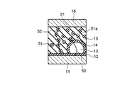
【解決手段】 第1の導電部11と、第1の導電部上に形成された第1のトンネル絶縁膜12と、第1のトンネル絶縁膜上に部分的に形成され、クーロンブロッケイド条件を満たす導電性微粒子13と、導電性微粒子の表面に形成された第2のトンネル絶縁膜14と、第1のトンネル絶縁膜及び第2のトンネル絶縁膜上に形成されたトラップ絶縁膜15と、トラップ絶縁膜上に形成された第2の導電部16と、を有するメモリ素子を備える。
【選択図】 図1
Description
図1は、本発明の第1の実施形態に係る不揮発性メモリ装置の構成を模式的に示した断面図である。
図4は、本発明の第2の実施形態に係る不揮発性メモリ装置の構成を模式的に示した断面図である。
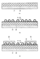
図6(a)〜図6(c)は、本実施形態に係る不揮発性メモリ装置の製造工程を示した断面図である。なお、途中の工程までは、図3に示した第1の実施形態の工程と同様であるため、図3の構成要素に対応する構成要素には同一の参照符号を付し、詳細な説明は省略する。
12、14、23、25、31、33…トンネル絶縁膜
13、24、32…導電性微粒子
15、22…トラップ絶縁膜
Claims (11)
- 第1の導電部と、
前記第1の導電部上に形成された第1のトンネル絶縁膜と、
前記第1のトンネル絶縁膜上に部分的に形成され、クーロンブロッケイド条件を満たす導電性微粒子と、
前記導電性微粒子の表面に形成された第2のトンネル絶縁膜と、
前記第1のトンネル絶縁膜及び第2のトンネル絶縁膜上に形成されたトラップ絶縁膜と、
前記トラップ絶縁膜上に形成された第2の導電部と、
を有するメモリ素子を備えたことを特徴とする不揮発性メモリ装置。 - 第1の導電部と、
前記第1の導電部上に形成されたトラップ絶縁膜と、
前記トラップ絶縁膜上に形成された第1のトンネル絶縁膜と、
前記第1のトンネル絶縁膜上に部分的に形成され、クーロンブロッケイド条件を満たす導電性微粒子と、
前記導電性微粒子の表面に形成された第2のトンネル絶縁膜と、
前記第1のトンネル絶縁膜及び第2のトンネル絶縁膜上に形成された第2の導電部と、
を有するメモリ素子を備えたことを特徴とする不揮発性メモリ装置。 - 第1の導電部と、
前記第1の導電部上に形成された第1のトンネル絶縁膜と、
前記第1のトンネル絶縁膜上に部分的に形成され、クーロンブロッケイド条件を満たす第1の導電性微粒子と、
前記第1の導電性微粒子の表面に形成された第2のトンネル絶縁膜と、
前記第1のトンネル絶縁膜及び第2のトンネル絶縁膜上に形成されたトラップ絶縁膜と、
前記トラップ絶縁膜上に形成された第3のトンネル絶縁膜と、
前記第3のトンネル絶縁膜上に部分的に形成され、クーロンブロッケイド条件を満たす第2の導電性微粒子と、
前記第2の導電性微粒子の表面に形成された第4のトンネル絶縁膜と、
前記第3のトンネル絶縁膜及び第4のトンネル絶縁膜上に形成された第2の導電部と、
を有するメモリ素子を備えたことを特徴とする不揮発性メモリ装置。 - 前記トラップ絶縁膜は、前記第1の導電部のパターンと前記第2の導電部のパターンがオーバーラップする領域に選択的に形成されている
ことを特徴とする請求項1乃至3のいずれかに記載の不揮発性メモリ装置。 - 前記トラップ絶縁膜は、化学量論比を満たすシリコン窒化膜のシリコン組成比よりも高いシリコン組成比を有するシリコン窒化膜、化学量論比を満たすシリコン酸化膜のシリコン組成比よりも高いシリコン組成比を有するシリコン酸化膜、又は化学量論比を満たすシリコン酸窒化膜のシリコン組成比よりも高いシリコン組成比を有するシリコン酸窒化膜で形成されている
ことを特徴とする請求項1乃至3のいずれかに記載の不揮発性メモリ装置。 - 前記トラップ絶縁膜のトラップ準位の密度は、1018cm-3以上である
ことを特徴とする請求項1乃至3のいずれかに記載の不揮発性メモリ装置。 - 前記トラップ絶縁膜のトラップ準位の密度は、前記トラップ絶縁膜の直接トンネル可能膜厚の上限をTとして、T-3以上である
ことを特徴とする請求項1乃至3のいずれかに記載の不揮発性メモリ装置。 - 前記トラップ絶縁膜の膜厚は、直接トンネル可能膜厚の上限以上である
ことを特徴とする請求項1乃至3のいずれかに記載の不揮発性メモリ装置。 - 前記トラップ絶縁膜の膜厚は、互いに隣接するメモリ素子間の間隔よりも小さい
ことを特徴とする請求項1乃至3のいずれかに記載の不揮発性メモリ装置。 - 前記導電性微粒子の密度は、2.5×1011cm-2以上である
ことを特徴とする請求項1又は2に記載の不揮発性メモリ装置。 - 前記第1のトンネル絶縁膜の膜厚は直接トンネル可能膜厚の上限以下であり、前記第2のトンネル絶縁膜の膜厚は直接トンネル可能膜厚の上限以下である
ことを特徴とする請求項1乃至3のいずれかに記載の不揮発性メモリ装置。
Priority Applications (1)
| Application Number | Priority Date | Filing Date | Title |
|---|---|---|---|
| JP2005005431A JP4247188B2 (ja) | 2005-01-12 | 2005-01-12 | 不揮発性メモリ装置 |
Applications Claiming Priority (1)
| Application Number | Priority Date | Filing Date | Title |
|---|---|---|---|
| JP2005005431A JP4247188B2 (ja) | 2005-01-12 | 2005-01-12 | 不揮発性メモリ装置 |
Publications (2)
| Publication Number | Publication Date |
|---|---|
| JP2006196601A true JP2006196601A (ja) | 2006-07-27 |
| JP4247188B2 JP4247188B2 (ja) | 2009-04-02 |
Family
ID=36802448
Family Applications (1)
| Application Number | Title | Priority Date | Filing Date |
|---|---|---|---|
| JP2005005431A Expired - Fee Related JP4247188B2 (ja) | 2005-01-12 | 2005-01-12 | 不揮発性メモリ装置 |
Country Status (1)
| Country | Link |
|---|---|
| JP (1) | JP4247188B2 (ja) |
Cited By (4)
| Publication number | Priority date | Publication date | Assignee | Title |
|---|---|---|---|---|
| KR100843229B1 (ko) | 2007-01-11 | 2008-07-02 | 삼성전자주식회사 | 하이브리드 구조의 전하 트랩막을 포함하는 플래쉬 메모리소자 및 그 제조 방법 |
| WO2009104229A1 (ja) * | 2008-02-19 | 2009-08-27 | パナソニック株式会社 | 抵抗変化型不揮発性メモリ素子とその作製方法 |
| JP2013077603A (ja) * | 2011-09-29 | 2013-04-25 | Toshiba Corp | メモリ装置 |
| US8969843B2 (en) | 2013-02-21 | 2015-03-03 | Kabushiki Kaisha Toshiba | Memory device |
-
2005
- 2005-01-12 JP JP2005005431A patent/JP4247188B2/ja not_active Expired - Fee Related
Cited By (6)
| Publication number | Priority date | Publication date | Assignee | Title |
|---|---|---|---|---|
| KR100843229B1 (ko) | 2007-01-11 | 2008-07-02 | 삼성전자주식회사 | 하이브리드 구조의 전하 트랩막을 포함하는 플래쉬 메모리소자 및 그 제조 방법 |
| WO2009104229A1 (ja) * | 2008-02-19 | 2009-08-27 | パナソニック株式会社 | 抵抗変化型不揮発性メモリ素子とその作製方法 |
| US7738280B2 (en) | 2008-02-19 | 2010-06-15 | Panasonic Corporation | Resistive nonvolatile memory element, and production method of the same |
| JP2013077603A (ja) * | 2011-09-29 | 2013-04-25 | Toshiba Corp | メモリ装置 |
| US9061898B2 (en) | 2011-09-29 | 2015-06-23 | Kabushiki Kaisha Toshiba | Memory device |
| US8969843B2 (en) | 2013-02-21 | 2015-03-03 | Kabushiki Kaisha Toshiba | Memory device |
Also Published As
| Publication number | Publication date |
|---|---|
| JP4247188B2 (ja) | 2009-04-02 |
Similar Documents
| Publication | Publication Date | Title |
|---|---|---|
| US6680505B2 (en) | Semiconductor storage element | |
| KR100688575B1 (ko) | 비휘발성 반도체 메모리 소자 | |
| JP4928773B2 (ja) | 半導体装置 | |
| US6670670B2 (en) | Single electron memory device comprising quantum dots between gate electrode and single electron storage element and method for manufacturing the same | |
| CN1574360B (zh) | 具有纳米晶体层的sonos存储器件 | |
| CN110431665A (zh) | 存储器单元及集成式结构 | |
| CN102473682B (zh) | 非易失性半导体存储器 | |
| JP5210675B2 (ja) | 不揮発性半導体記憶装置及びその製造方法 | |
| JP5531252B2 (ja) | 不揮発性半導体メモリ | |
| JP3580781B2 (ja) | 半導体記憶素子 | |
| JP2010245345A (ja) | 不揮発性半導体メモリ及びその製造方法 | |
| JP4253473B2 (ja) | 半導体装置及びその製造方法 | |
| WO2010087265A1 (ja) | 不揮発性半導体記憶装置およびその製造方法 | |
| JPWO2008146760A1 (ja) | 記憶素子及びその読み出し方法 | |
| CN101111943A (zh) | 非易失性存储装置及其制造方法 | |
| JP2005277263A (ja) | 量子ドット電界効果トランジスタ、それを用いたメモリ素子及び光センサ及びそれらの集積回路 | |
| JP4247188B2 (ja) | 不揮発性メモリ装置 | |
| JP3469212B2 (ja) | 半導体記憶素子 | |
| US7217620B2 (en) | Methods of forming silicon quantum dots and methods of fabricating semiconductor memory device using the same | |
| JP3378386B2 (ja) | 半導体記憶装置 | |
| JP4719267B2 (ja) | 半導体装置 | |
| JP2013077603A (ja) | メモリ装置 | |
| CN1964076A (zh) | 使用纳米点作为俘获位的半导体存储器件及其制造方法 | |
| JPS6055669A (ja) | 不揮発性半導体メモリ素子 | |
| JP5297556B2 (ja) | 不揮発性半導体記憶装置 |
Legal Events
| Date | Code | Title | Description |
|---|---|---|---|
| A977 | Report on retrieval |
Free format text: JAPANESE INTERMEDIATE CODE: A971007 Effective date: 20080925 |
|
| A131 | Notification of reasons for refusal |
Free format text: JAPANESE INTERMEDIATE CODE: A131 Effective date: 20081007 |
|
| A521 | Request for written amendment filed |
Free format text: JAPANESE INTERMEDIATE CODE: A523 Effective date: 20081203 |
|
| TRDD | Decision of grant or rejection written | ||
| A01 | Written decision to grant a patent or to grant a registration (utility model) |
Free format text: JAPANESE INTERMEDIATE CODE: A01 Effective date: 20090106 |
|
| A01 | Written decision to grant a patent or to grant a registration (utility model) |
Free format text: JAPANESE INTERMEDIATE CODE: A01 |
|
| A61 | First payment of annual fees (during grant procedure) |
Free format text: JAPANESE INTERMEDIATE CODE: A61 Effective date: 20090109 |
|
| FPAY | Renewal fee payment (event date is renewal date of database) |
Free format text: PAYMENT UNTIL: 20120116 Year of fee payment: 3 |
|
| FPAY | Renewal fee payment (event date is renewal date of database) |
Free format text: PAYMENT UNTIL: 20130116 Year of fee payment: 4 |
|
| FPAY | Renewal fee payment (event date is renewal date of database) |
Free format text: PAYMENT UNTIL: 20130116 Year of fee payment: 4 |
|
| FPAY | Renewal fee payment (event date is renewal date of database) |
Free format text: PAYMENT UNTIL: 20140116 Year of fee payment: 5 |
|
| LAPS | Cancellation because of no payment of annual fees |