JP2006196631A - 半導体装置及びその製造方法 - Google Patents
半導体装置及びその製造方法 Download PDFInfo
- Publication number
- JP2006196631A JP2006196631A JP2005005841A JP2005005841A JP2006196631A JP 2006196631 A JP2006196631 A JP 2006196631A JP 2005005841 A JP2005005841 A JP 2005005841A JP 2005005841 A JP2005005841 A JP 2005005841A JP 2006196631 A JP2006196631 A JP 2006196631A
- Authority
- JP
- Japan
- Prior art keywords
- semiconductor
- layer
- substrate
- semiconductor substrate
- buffer layer
- Prior art date
- Legal status (The legal status is an assumption and is not a legal conclusion. Google has not performed a legal analysis and makes no representation as to the accuracy of the status listed.)
- Pending
Links
Images


Classifications
-
- H—ELECTRICITY
- H10—SEMICONDUCTOR DEVICES; ELECTRIC SOLID-STATE DEVICES NOT OTHERWISE PROVIDED FOR
- H10P—GENERIC PROCESSES OR APPARATUS FOR THE MANUFACTURE OR TREATMENT OF DEVICES COVERED BY CLASS H10
- H10P14/00—Formation of materials, e.g. in the shape of layers or pillars
- H10P14/20—Formation of materials, e.g. in the shape of layers or pillars of semiconductor materials
- H10P14/24—Formation of materials, e.g. in the shape of layers or pillars of semiconductor materials using chemical vapour deposition [CVD]
-
- H—ELECTRICITY
- H10—SEMICONDUCTOR DEVICES; ELECTRIC SOLID-STATE DEVICES NOT OTHERWISE PROVIDED FOR
- H10P—GENERIC PROCESSES OR APPARATUS FOR THE MANUFACTURE OR TREATMENT OF DEVICES COVERED BY CLASS H10
- H10P14/00—Formation of materials, e.g. in the shape of layers or pillars
- H10P14/20—Formation of materials, e.g. in the shape of layers or pillars of semiconductor materials
- H10P14/29—Formation of materials, e.g. in the shape of layers or pillars of semiconductor materials characterised by the substrates
- H10P14/2901—Materials
- H10P14/2902—Materials being Group IVA materials
- H10P14/2905—Silicon, silicon germanium or germanium
-
- H—ELECTRICITY
- H10—SEMICONDUCTOR DEVICES; ELECTRIC SOLID-STATE DEVICES NOT OTHERWISE PROVIDED FOR
- H10P—GENERIC PROCESSES OR APPARATUS FOR THE MANUFACTURE OR TREATMENT OF DEVICES COVERED BY CLASS H10
- H10P14/00—Formation of materials, e.g. in the shape of layers or pillars
- H10P14/20—Formation of materials, e.g. in the shape of layers or pillars of semiconductor materials
- H10P14/29—Formation of materials, e.g. in the shape of layers or pillars of semiconductor materials characterised by the substrates
- H10P14/2924—Structures
- H10P14/2925—Surface structures
-
- H—ELECTRICITY
- H10—SEMICONDUCTOR DEVICES; ELECTRIC SOLID-STATE DEVICES NOT OTHERWISE PROVIDED FOR
- H10P—GENERIC PROCESSES OR APPARATUS FOR THE MANUFACTURE OR TREATMENT OF DEVICES COVERED BY CLASS H10
- H10P14/00—Formation of materials, e.g. in the shape of layers or pillars
- H10P14/20—Formation of materials, e.g. in the shape of layers or pillars of semiconductor materials
- H10P14/29—Formation of materials, e.g. in the shape of layers or pillars of semiconductor materials characterised by the substrates
- H10P14/2926—Crystal orientations
-
- H—ELECTRICITY
- H10—SEMICONDUCTOR DEVICES; ELECTRIC SOLID-STATE DEVICES NOT OTHERWISE PROVIDED FOR
- H10P—GENERIC PROCESSES OR APPARATUS FOR THE MANUFACTURE OR TREATMENT OF DEVICES COVERED BY CLASS H10
- H10P14/00—Formation of materials, e.g. in the shape of layers or pillars
- H10P14/20—Formation of materials, e.g. in the shape of layers or pillars of semiconductor materials
- H10P14/32—Formation of materials, e.g. in the shape of layers or pillars of semiconductor materials characterised by intermediate layers between substrates and deposited layers
- H10P14/3202—Materials thereof
- H10P14/3204—Materials thereof being Group IVA semiconducting materials
- H10P14/3208—Silicon carbide
-
- H—ELECTRICITY
- H10—SEMICONDUCTOR DEVICES; ELECTRIC SOLID-STATE DEVICES NOT OTHERWISE PROVIDED FOR
- H10P—GENERIC PROCESSES OR APPARATUS FOR THE MANUFACTURE OR TREATMENT OF DEVICES COVERED BY CLASS H10
- H10P14/00—Formation of materials, e.g. in the shape of layers or pillars
- H10P14/20—Formation of materials, e.g. in the shape of layers or pillars of semiconductor materials
- H10P14/32—Formation of materials, e.g. in the shape of layers or pillars of semiconductor materials characterised by intermediate layers between substrates and deposited layers
- H10P14/3202—Materials thereof
- H10P14/3204—Materials thereof being Group IVA semiconducting materials
- H10P14/3211—Silicon, silicon germanium or germanium
-
- H—ELECTRICITY
- H10—SEMICONDUCTOR DEVICES; ELECTRIC SOLID-STATE DEVICES NOT OTHERWISE PROVIDED FOR
- H10P—GENERIC PROCESSES OR APPARATUS FOR THE MANUFACTURE OR TREATMENT OF DEVICES COVERED BY CLASS H10
- H10P14/00—Formation of materials, e.g. in the shape of layers or pillars
- H10P14/20—Formation of materials, e.g. in the shape of layers or pillars of semiconductor materials
- H10P14/32—Formation of materials, e.g. in the shape of layers or pillars of semiconductor materials characterised by intermediate layers between substrates and deposited layers
- H10P14/3242—Structure
- H10P14/3244—Layer structure
- H10P14/3248—Layer structure consisting of two layers
-
- H—ELECTRICITY
- H10—SEMICONDUCTOR DEVICES; ELECTRIC SOLID-STATE DEVICES NOT OTHERWISE PROVIDED FOR
- H10P—GENERIC PROCESSES OR APPARATUS FOR THE MANUFACTURE OR TREATMENT OF DEVICES COVERED BY CLASS H10
- H10P14/00—Formation of materials, e.g. in the shape of layers or pillars
- H10P14/20—Formation of materials, e.g. in the shape of layers or pillars of semiconductor materials
- H10P14/32—Formation of materials, e.g. in the shape of layers or pillars of semiconductor materials characterised by intermediate layers between substrates and deposited layers
- H10P14/3242—Structure
- H10P14/3244—Layer structure
- H10P14/3251—Layer structure consisting of three or more layers
-
- H—ELECTRICITY
- H10—SEMICONDUCTOR DEVICES; ELECTRIC SOLID-STATE DEVICES NOT OTHERWISE PROVIDED FOR
- H10P—GENERIC PROCESSES OR APPARATUS FOR THE MANUFACTURE OR TREATMENT OF DEVICES COVERED BY CLASS H10
- H10P14/00—Formation of materials, e.g. in the shape of layers or pillars
- H10P14/20—Formation of materials, e.g. in the shape of layers or pillars of semiconductor materials
- H10P14/34—Deposited materials, e.g. layers
- H10P14/3402—Deposited materials, e.g. layers characterised by the chemical composition
- H10P14/3404—Deposited materials, e.g. layers characterised by the chemical composition being Group IVA materials
- H10P14/3408—Silicon carbide
-
- H—ELECTRICITY
- H10—SEMICONDUCTOR DEVICES; ELECTRIC SOLID-STATE DEVICES NOT OTHERWISE PROVIDED FOR
- H10H—INORGANIC LIGHT-EMITTING SEMICONDUCTOR DEVICES HAVING POTENTIAL BARRIERS
- H10H20/00—Individual inorganic light-emitting semiconductor devices having potential barriers, e.g. light-emitting diodes [LED]
- H10H20/80—Constructional details
- H10H20/81—Bodies
- H10H20/815—Bodies having stress relaxation structures, e.g. buffer layers
Landscapes
- Recrystallisation Techniques (AREA)
- Led Devices (AREA)
Abstract
【解決手段】基板の面方位に対して鏡面対称なファセットの対が複数上部に形成されたSi基板上に、Siを一部含み、且つ前記Si基板より欠陥密度が多い半導体緩衝層を形成し、この上にSiC層を順次形成させることにより半導体装置を作成する。
【効果】半導体緩衝層内に発生した欠陥は、Si基板に垂直な軸、すなわち、基板の面方位に対して鏡面対称な対を持ち、対向する欠陥同士は会合・消滅する。上記緩衝層には炭化珪素層に比べて欠陥を生じ易い性質を持たせており、欠陥を緩衝層内部に内包させることが出来る。特定箇所に欠陥を高確率で発生させることで歪緩和を促進し、且つ上記欠陥の進行を制御することで欠陥を消滅させ、無歪み且つ低欠陥密度のSiC層の形成が可能となる。
【選択図】図1
Description
この目的のため、本発明の半導体装置は対向するファセットの対が複数上部に配列された半導体基板と、該半導体基板上に設けられ、前記半導体基板より欠陥密度が多い半導体緩衝層と、該半導体緩衝層上に設けられ、格子定数が前記半導体基板と異なり、前記半導体基板の構成元素と異なる元素を含有した第1の半導体層を有し、前記ファセットは前記半導体基板の面方位とは異なる面方位を有し、且つ対向する二つのファセットからなるそれぞれのファセット対は前記半導体基板の面方位に対して鏡面対称であることを特徴としている。
前記半導体基板が(001)面の面方位を有し、対向する前記ファセットはそれぞれ(111)面と(-1-11)面、(-111)面と(1-11)面から成り、前記ファセットで囲まれる領域は前記半導体基板表面において矩形のパターンを形成しており、前記半導体緩衝層は半導体基板全面に形成されていれば良い。
更に好適な例としては、前記半導体緩衝層の機械的強度または原子間結合エネルギーは、前記第1の半導体層の機械的強度または原子間結合エネルギーに比べて小さいと良い。
前記半導体緩衝層のもう一つの例として、前記半導体緩衝層は、機械的強度または原子間結合エネルギーが前記第1の半導体層の機械的強度または原子間結合エネルギーより小さい第1の半導体緩衝層と、該第1の半導体緩衝層よりも機械的強度または原子間結合エネルギーが大きい第2の半導体緩衝層が交互に繰り返された多層構造であっても良い。
本発明に係わるもう一つの好適例として、前記第1の半導体層上に、窒素を含む複数のIII-V族化合物半導体層からなる第2の半導体層が設けられ、該第2の半導体層上および/または前記第1の半導体層上および/または前記半導体基板上に電子デバイスもしくは発光素子を設けていると良い。
前記半導体基板がシリコンからなり、前記半導体緩衝層がシリコンとゲルマニウムと炭素を含んだ材料からなり、前記第1の半導体層がシリコンと炭素の結合を含む化合物半導体からなると好適である。
前記半導体緩衝層及び前記第1の半導体層を気相成長法により形成すると好適である。
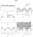
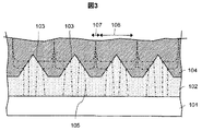
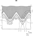
図1は、本発明に係る半導体薄膜の第1の実施例を示す断面図である。単結晶シリコン(Si)基板1上には、一列に配列した一組のファセット2と2'が複数形成されている。なお、このファセットが形成される基板表面での貫通転位密度は1個/cm2未満である。この時、対向するファセット2と2'は基板と垂直な軸、すなわち、基板の面方位に対して鏡面対称な形状を有している。また、本実施例ではファセット同士で形成される溝底部と隣り合う溝の間には、基板の面方位と同じ面を有する平坦部3が存在している。この平坦部はファセット形成時に必ずしも存在している必要は無いが、図1のように予め形成しておいたほうが望ましい。平坦部が無い場合の例に関しては製造法のところで後述する。図1はSi (001)基板を用いた場合の例を示しており、この時、対向するファセットはそれぞれ(111)、(-1-11)面となる。Si基板1上には、Siを材料の一部として含む緩衝層4が形成され、更に炭化珪素(SiC)層5が形成されている。緩衝層4としては、SiC層5に比べて機械的強度が弱いか、もしくは原子間結合エネルギーの小さい材質を用いると良い。ここでは、例えば炭化または低温成長により形成したSiC層、またはSi-C結合より結合エネルギーが小さいGe-C結合を含むシリコン・ゲルマニウム・カーバイド(SiGeC)層を用いることが可能である。
Claims (24)
- 対向するファセットの対が複数上部に配列された半導体基板と、該半導体基板上に設けられ、前記半導体基板より欠陥密度が多い半導体緩衝層と、該半導体緩衝層上に設けられ、格子定数が前記半導体基板と異なり、前記半導体基板の構成元素と異なる元素を含有した第1の半導体層を有し、前記ファセットは前記半導体基板の面方位とは異なる面方位を有し、且つ対向する二つのファセットからなるそれぞれのファセット対は前記半導体基板の面方位に対して鏡面対称であることを特徴とする半導体装置。
- 前記半導体緩衝層と前記第1の半導体層の内部において、前記半導体基板の面方位に対して鏡面対称な欠陥の対が複数存在しており、前記各層内部の欠陥の数は、前記第1の半導体層の表面に向かって数が減少していることを特徴とする請求項1に記載の半導体装置。
- 前記半導体緩衝層の機械的強度または原子間結合エネルギーは、前記第1の半導体層の機械的強度または原子間結合エネルギーに比べて小さいことを特徴とする請求項1に記載の半導体装置。
- 前記半導体緩衝層は、複数の元素の組成が異なる層で構成され、前記半導体基板から前記第1の半導体層に近づくに従って、前記元素の組成が段階的に前記第1の半導体層の元素の組成に近づくことを特徴とする請求項1に記載の半導体装置。
- 前記半導体緩衝層は、機械的強度または原子間結合エネルギーが前記第1の半導体層の機械的強度または原子間結合エネルギーより小さい第1の半導体緩衝層と、該第1の半導体緩衝層よりも機械的強度または原子間結合エネルギーが大きい第2の半導体緩衝層が交互に繰り返された多層構造であることを特徴とする請求項1に記載の半導体装置。
- 前記第1の半導体層上に電子デバイスもしくは発光素子を設けたことを特徴とする請求項1に記載の半導体装置。
- 前記第1の半導体層上に、窒素を含む複数のIII-V族化合物半導体層からなる第2の半導体層が設けられ、該第2の半導体層上および/または前記第1の半導体層上および/または前記半導体基板上に電子デバイスもしくは発光素子を設けたことを特徴とする請求項1に記載の半導体装置。
- 前記半導体基板がシリコンからなり、前記半導体緩衝層がシリコンとゲルマニウムと炭素を含んだ材料からなり、前記第1の半導体層がシリコンと炭素の結合を含む化合物半導体からなることを特徴とする請求項1に記載の半導体装置。
- 互いに垂直な方位に沿って、対向するファセットの対が複数上部に配列された半導体基板と、該半導体基板上に設けられ、前記半導体基板より欠陥密度が多い半導体緩衝層と、該半導体緩衝層上に設けられ、格子定数が前記半導体基板と異なり、前記半導体基板の構成元素と異なる元素を含有した第1の半導体層を有し、前記ファセットは前記半導体基板の面方位とは異なる面方位を有し、且つ対向する二つのファセットからなるそれぞれのファセット対は前記半導体基板の面方位に対して鏡面対称であることを特徴とする半導体装置。
- 前記互いに垂直な方位が、[-110]と[110]、[-1-12]と[-110]であることを特徴とする請求項9に記載の半導体装置。
- 前記半導体基板が(001)面の面方位を有し、対向する前記ファセットはそれぞれ(111)面と(-1-11)面、(-111)面と(1-11)面から成り、前記ファセットで囲まれる領域は前記半導体基板表面において矩形のパターンを形成しており、前記半導体緩衝層は半導体基板全面に形成されていることを特徴とする請求項9に記載の半導体装置。
- 前記半導体基板が(111)面の面方位を有し、対向する前記ファセットはそれぞれ(1-10)面と(-110)面、(11-2)面と(-1-12)面から成り、前記ファセットで囲まれる領域は前記半導体基板表面において矩形のパターンを形成しており、前記半導体緩衝層は半導体基板全面に形成されていることを特徴とする請求項9に記載の半導体装置。
- 前記半導体緩衝層と前記第1の半導体層の内部において、前記半導体基板の面方位に対して鏡面対称な欠陥の対が複数存在しており、前記各層内部の欠陥の数は、前記第1の半導体層の表面に向かって数が減少していることを特徴とする請求項9に記載の半導体装置。
- 前記半導体緩衝層の機械的強度または原子間結合エネルギーは、前記第1の半導体層の機械的強度または原子間結合エネルギーに比べて小さいことを特徴とする請求項9に記載の半導体装置。
- 前記半導体緩衝層は、複数の元素の組成が異なる層で構成され、前記半導体基板から前記第1の半導体層に近づくに従って前記元素の組成が段階的に前記第1の半導体層の元素の組成に近づくことを特徴とする請求項9に記載の半導体装置。
- 前記半導体緩衝層は、機械的強度または原子間結合エネルギーが前記第1の半導体層の機械的強度または原子間結合エネルギーより小さい第1の半導体緩衝層と、該第1の半導体緩衝層よりも機械的強度または原子間結合エネルギーが大きい第2の半導体緩衝層が交互に繰り返された多層構造であることを特徴とする請求項9に記載の半導体装置。
- 前記第1の半導体層上に電子デバイスもしくは発光素子を設けたことを特徴とする請求項9に記載の半導体装置。
- 前記第1の半導体層上に、窒素を含む複数のIII-V族化合物半導体層からなる第2の半導体層が設けられ、該第2の半導体層上および/または前記第1の半導体層上および/または前記半導体基板上に電子デバイスもしくは発光素子を設けたことを特徴とする請求項9に記載の半導体装置。
- 前記半導体基板がシリコンからなり、前記半導体緩衝層がシリコンとゲルマニウムと炭素を含んだ材料からなり、前記第1の半導体層がシリコンと炭素の結合を含む化合物半導体からなることを特徴とする請求項9に記載の半導体装置。
- 半導体基板の面方位に対して鏡面対称なファセットの対が複数上部に形成されたSi基板上に、Siを一部含み、且つ前記Si基板より欠陥密度が多い半導体緩衝層を形成し、この上にSiC層を順次形成させた半導体装置。
- 半導体基板上に、対向するファセットの対を複数形成する工程と、前記半導体基板の少なくとも一部領域上に前記半導体基板より欠陥密度が多い半導体緩衝層を一層以上形成する工程と、該半導体緩衝層の少なくとも一部領域上に格子定数が前記半導体基板と異なり、前記半導体基板の構成元素と異なる元素を含有した第1の半導体層を形成する工程を有し、前記ファセットは前記半導体基板の面方位とは異なる面方位を有し、且つ対向する二つのファセットからなるそれぞれのファセット対は前記半導体基板の面方位に対して鏡面対称であることを特徴とする半導体装置の製造方法。
- 前記半導体緩衝層及び前記第1の半導体層を気相成長法により形成することを特徴とする請求項21に記載の半導体装置の製造方法。
- 互いに垂直な方位に沿って、半導体基板上に、対向するファセットの対を複数形成する工程と、前記半導体基板の少なくとも一部領域上に前記半導体基板より欠陥密度が多い半導体緩衝層を一層以上形成する工程と、該半導体緩衝層の少なくとも一部領域上に格子定数が前記半導体基板と異なり、前記半導体基板の構成元素と異なる元素を含有した第1の半導体層を形成する工程を有し、前記ファセットは前記半導体基板の面方位とは異なる面方位を有し、且つ対向する二つのファセットからなるそれぞれのファセット対は前記半導体基板の面方位に対して鏡面対称であることを特徴とする半導体装置の製造方法。
- 前記半導体緩衝層及び前記第1の半導体層を気相成長法により形成することを特徴とする請求項23に記載の半導体装置の製造方法。
Priority Applications (2)
| Application Number | Priority Date | Filing Date | Title |
|---|---|---|---|
| JP2005005841A JP2006196631A (ja) | 2005-01-13 | 2005-01-13 | 半導体装置及びその製造方法 |
| US11/072,279 US7368763B2 (en) | 2005-01-13 | 2005-03-07 | Semiconductor device and manufacturing method thereof |
Applications Claiming Priority (1)
| Application Number | Priority Date | Filing Date | Title |
|---|---|---|---|
| JP2005005841A JP2006196631A (ja) | 2005-01-13 | 2005-01-13 | 半導体装置及びその製造方法 |
Publications (1)
| Publication Number | Publication Date |
|---|---|
| JP2006196631A true JP2006196631A (ja) | 2006-07-27 |
Family
ID=36755576
Family Applications (1)
| Application Number | Title | Priority Date | Filing Date |
|---|---|---|---|
| JP2005005841A Pending JP2006196631A (ja) | 2005-01-13 | 2005-01-13 | 半導体装置及びその製造方法 |
Country Status (2)
| Country | Link |
|---|---|
| US (1) | US7368763B2 (ja) |
| JP (1) | JP2006196631A (ja) |
Cited By (7)
| Publication number | Priority date | Publication date | Assignee | Title |
|---|---|---|---|---|
| JP2011225421A (ja) * | 2010-03-29 | 2011-11-10 | Air Water Inc | 単結晶3C−SiC基板の製造方法およびそれによって得られた単結晶3C−SiC基板 |
| JP2012028494A (ja) * | 2010-07-22 | 2012-02-09 | Seiko Epson Corp | 単結晶炭化珪素膜付き基材及び単結晶炭化珪素膜の製造方法並びに単結晶炭化珪素膜付き基材の製造方法 |
| WO2012105179A1 (ja) * | 2011-02-03 | 2012-08-09 | 次世代パワーデバイス技術研究組合 | 半導体基板、半導体装置、および半導体基板の製造方法 |
| KR20160055939A (ko) * | 2013-10-31 | 2016-05-18 | 고쿠리츠켄큐카이하츠호진 카가쿠기쥬츠신코키코 | Iii-v족 화합물 반도체 나노와이어, 전계효과 트랜지스터 및 스위치 소자 |
| WO2019009182A1 (ja) * | 2017-07-07 | 2019-01-10 | セイコーエプソン株式会社 | 単結晶基板、単結晶基板の製造方法および炭化ケイ素基板 |
| WO2019009183A1 (ja) * | 2017-07-07 | 2019-01-10 | セイコーエプソン株式会社 | 単結晶基板、単結晶基板の製造方法および炭化ケイ素基板 |
| WO2019009181A1 (ja) * | 2017-07-07 | 2019-01-10 | セイコーエプソン株式会社 | 単結晶基板および炭化ケイ素基板 |
Families Citing this family (69)
| Publication number | Priority date | Publication date | Assignee | Title |
|---|---|---|---|---|
| JP2006027929A (ja) * | 2004-07-13 | 2006-02-02 | Toshiba Ceramics Co Ltd | 電気光学的単結晶薄膜成長用基板及びその製造方法 |
| KR100664988B1 (ko) | 2004-11-04 | 2007-01-09 | 삼성전기주식회사 | 광추출효율이 향상된 반도체 발광소자 |
| US9153645B2 (en) * | 2005-05-17 | 2015-10-06 | Taiwan Semiconductor Manufacturing Company, Ltd. | Lattice-mismatched semiconductor structures with reduced dislocation defect densities and related methods for device fabrication |
| US8324660B2 (en) | 2005-05-17 | 2012-12-04 | Taiwan Semiconductor Manufacturing Company, Ltd. | Lattice-mismatched semiconductor structures with reduced dislocation defect densities and related methods for device fabrication |
| JP2007201336A (ja) * | 2006-01-30 | 2007-08-09 | Hitachi Ltd | 半導体積層体の形成方法 |
| US7777250B2 (en) | 2006-03-24 | 2010-08-17 | Taiwan Semiconductor Manufacturing Company, Ltd. | Lattice-mismatched semiconductor structures and related methods for device fabrication |
| US8173551B2 (en) | 2006-09-07 | 2012-05-08 | Taiwan Semiconductor Manufacturing Co., Ltd. | Defect reduction using aspect ratio trapping |
| US7875958B2 (en) | 2006-09-27 | 2011-01-25 | Taiwan Semiconductor Manufacturing Company, Ltd. | Quantum tunneling devices and circuits with lattice-mismatched semiconductor structures |
| US20080187018A1 (en) | 2006-10-19 | 2008-08-07 | Amberwave Systems Corporation | Distributed feedback lasers formed via aspect ratio trapping |
| US8304805B2 (en) | 2009-01-09 | 2012-11-06 | Taiwan Semiconductor Manufacturing Company, Ltd. | Semiconductor diodes fabricated by aspect ratio trapping with coalesced films |
| US9508890B2 (en) | 2007-04-09 | 2016-11-29 | Taiwan Semiconductor Manufacturing Company, Ltd. | Photovoltaics on silicon |
| US8237151B2 (en) | 2009-01-09 | 2012-08-07 | Taiwan Semiconductor Manufacturing Company, Ltd. | Diode-based devices and methods for making the same |
| US7825328B2 (en) | 2007-04-09 | 2010-11-02 | Taiwan Semiconductor Manufacturing Company, Ltd. | Nitride-based multi-junction solar cell modules and methods for making the same |
| US7956370B2 (en) * | 2007-06-12 | 2011-06-07 | Siphoton, Inc. | Silicon based solid state lighting |
| US20090032799A1 (en) * | 2007-06-12 | 2009-02-05 | Siphoton, Inc | Light emitting device |
| US8329541B2 (en) | 2007-06-15 | 2012-12-11 | Taiwan Semiconductor Manufacturing Company, Ltd. | InP-based transistor fabrication |
| US7888248B2 (en) * | 2007-07-13 | 2011-02-15 | Northrop Grumman Systems Corporation | Method of producing large area SiC substrates |
| WO2009035746A2 (en) | 2007-09-07 | 2009-03-19 | Amberwave Systems Corporation | Multi-junction solar cells |
| JP2009260296A (ja) * | 2008-03-18 | 2009-11-05 | Hitachi Cable Ltd | 窒化物半導体エピタキシャルウエハ及び窒化物半導体素子 |
| US8183667B2 (en) | 2008-06-03 | 2012-05-22 | Taiwan Semiconductor Manufacturing Co., Ltd. | Epitaxial growth of crystalline material |
| US20110108800A1 (en) * | 2008-06-24 | 2011-05-12 | Pan Shaoher X | Silicon based solid state lighting |
| US8274097B2 (en) | 2008-07-01 | 2012-09-25 | Taiwan Semiconductor Manufacturing Company, Ltd. | Reduction of edge effects from aspect ratio trapping |
| US8981427B2 (en) | 2008-07-15 | 2015-03-17 | Taiwan Semiconductor Manufacturing Company, Ltd. | Polishing of small composite semiconductor materials |
| US20110114917A1 (en) * | 2008-07-21 | 2011-05-19 | Pan Shaoher X | Light emitting device |
| WO2010033813A2 (en) | 2008-09-19 | 2010-03-25 | Amberwave System Corporation | Formation of devices by epitaxial layer overgrowth |
| US20100072515A1 (en) | 2008-09-19 | 2010-03-25 | Amberwave Systems Corporation | Fabrication and structures of crystalline material |
| US8253211B2 (en) | 2008-09-24 | 2012-08-28 | Taiwan Semiconductor Manufacturing Company, Ltd. | Semiconductor sensor structures with reduced dislocation defect densities |
| US8313967B1 (en) | 2009-01-21 | 2012-11-20 | Stc.Unm | Cubic phase, nitrogen-based compound semiconductor films epitaxially grown on a grooved Si <001> substrate |
| KR20100093872A (ko) * | 2009-02-17 | 2010-08-26 | 삼성엘이디 주식회사 | 질화물 반도체 발광소자 및 그 제조방법 |
| SG171987A1 (en) | 2009-04-02 | 2011-07-28 | Taiwan Semiconductor Mfg | Devices formed from a non-polar plane of a crystalline material and method of making the same |
| US20100308300A1 (en) * | 2009-06-08 | 2010-12-09 | Siphoton, Inc. | Integrated circuit light emission device, module and fabrication process |
| US8350273B2 (en) | 2009-08-31 | 2013-01-08 | Infineon Technologies Ag | Semiconductor structure and a method of forming the same |
| US8722441B2 (en) * | 2010-01-21 | 2014-05-13 | Siphoton Inc. | Manufacturing process for solid state lighting device on a conductive substrate |
| US8674383B2 (en) * | 2010-01-21 | 2014-03-18 | Siphoton Inc. | Solid state lighting device on a conductive substrate |
| US8283676B2 (en) * | 2010-01-21 | 2012-10-09 | Siphoton Inc. | Manufacturing process for solid state lighting device on a conductive substrate |
| JP2011243848A (ja) * | 2010-05-20 | 2011-12-01 | Sumitomo Electric Ind Ltd | 炭化珪素基板の製造方法 |
| WO2011145283A1 (ja) * | 2010-05-20 | 2011-11-24 | パナソニック株式会社 | 窒化物半導体発光素子および窒化物半導体発光素子の製造方法 |
| US9184050B2 (en) | 2010-07-30 | 2015-11-10 | Taiwan Semiconductor Manufacturing Company, Ltd. | Inverted trapezoidal recess for epitaxial growth |
| CN102376835B (zh) * | 2010-08-23 | 2015-06-10 | 展晶科技(深圳)有限公司 | 外延基板 |
| US9269776B2 (en) * | 2011-01-25 | 2016-02-23 | Lg Innotek Co., Ltd. | Semiconductor device and method for growing semiconductor crystal |
| US8217418B1 (en) | 2011-02-14 | 2012-07-10 | Siphoton Inc. | Semi-polar semiconductor light emission devices |
| US8624292B2 (en) | 2011-02-14 | 2014-01-07 | Siphoton Inc. | Non-polar semiconductor light emission devices |
| US10164082B2 (en) * | 2012-05-04 | 2018-12-25 | Stc.Unm | Growth of cubic crystalline phase structure on silicon substrates and devices comprising the cubic crystalline phase structure |
| US10453996B2 (en) * | 2012-05-04 | 2019-10-22 | Stc.Unm | Growth of cubic crystalline phase structure on silicon substrates and devices comprising the cubic crystalline phase structure |
| US9520472B2 (en) | 2012-05-04 | 2016-12-13 | Stc.Unm | Growth of cubic crystalline phase strucure on silicon substrates and devices comprising the cubic crystalline phase structure |
| TWI482276B (zh) * | 2012-10-12 | 2015-04-21 | 財團法人工業技術研究院 | 氮化物半導體結構 |
| US9196709B2 (en) * | 2013-02-01 | 2015-11-24 | Taiwan Semiconductor Manufacturing Company, Ltd. | Methods for forming semiconductor regions in trenches |
| US9123633B2 (en) * | 2013-02-01 | 2015-09-01 | Taiwan Semiconductor Manufacturing Company, Ltd. | Methods for forming semiconductor regions in trenches |
| US9275861B2 (en) * | 2013-06-26 | 2016-03-01 | Globalfoundries Inc. | Methods of forming group III-V semiconductor materials on group IV substrates and the resulting substrate structures |
| GB2529953B (en) * | 2013-06-28 | 2020-04-01 | Intel Corp | Nanostructures and nanofeatures with Si (111) planes on Si (100) wafers for III-N epitaxy |
| JP5997373B2 (ja) * | 2013-08-21 | 2016-09-28 | シャープ株式会社 | 窒化物半導体発光素子 |
| KR102099193B1 (ko) * | 2013-09-27 | 2020-04-09 | 인텔 코포레이션 | 실리콘 핀들 상에서의 led 구조체들의 형성 |
| US9419138B2 (en) | 2014-09-29 | 2016-08-16 | International Business Machines Corporation | Embedded carbon-doped germanium as stressor for germanium nFET devices |
| CN106848015B (zh) * | 2017-03-08 | 2019-03-15 | 王星河 | 一种氮化物半导体发光二极管及其制作方法 |
| USD837914S1 (en) | 2017-09-15 | 2019-01-08 | Karsten Manufacturing Corporation | Golf club head |
| US11088189B2 (en) | 2017-11-14 | 2021-08-10 | Taiwan Semiconductor Manufacturing Co., Ltd. | High light absorption structure for semiconductor image sensor |
| US10818778B2 (en) * | 2017-11-27 | 2020-10-27 | Taiwan Semiconductor Manufacturing Co., Ltd. | Heterogeneous semiconductor device substrates with high quality epitaxy |
| CN111146320A (zh) * | 2018-11-02 | 2020-05-12 | 华为技术有限公司 | 硅基衬底、衬底基板及其制造方法、光电器件 |
| JP7393900B2 (ja) * | 2019-09-24 | 2023-12-07 | 一般財団法人電力中央研究所 | 炭化珪素単結晶ウェハ及び炭化珪素単結晶インゴットの製造方法 |
| EP3828918B1 (en) * | 2019-11-29 | 2025-06-11 | Imec VZW | Low parasitic ccb heterojunction bipolar transistor |
| US11515408B2 (en) * | 2020-03-02 | 2022-11-29 | Taiwan Semiconductor Manufacturing Company, Ltd. | Rough buffer layer for group III-V devices on silicon |
| US12598782B2 (en) | 2021-08-26 | 2026-04-07 | IceMos Technology Limited | Super-junction MOSFET/IGBT with MEMS layer transfer and WBG drain |
| US20230061047A1 (en) * | 2021-08-26 | 2023-03-02 | IceMos Technology Limited | Semiconductor Device and Method of Forming Sacrificial Heteroepitaxy Interface to Provide Substantially Defect-Free Silicon Carbide Substrate |
| US12506006B2 (en) | 2021-08-26 | 2025-12-23 | IceMos Technology Limited | Semiconductor device and method of direct wafer bonding between semiconductor layer containing similar WBG materials |
| CN115995389A (zh) * | 2021-10-20 | 2023-04-21 | 苏州晶湛半导体有限公司 | 射频器件、碳化硅同质外延衬底及其制作方法 |
| US20240047207A1 (en) * | 2022-08-02 | 2024-02-08 | Infineon Technologies Ag | Technique for Forming Cubic Silicon Carbide and Heterojunction Silicon Carbide Device |
| WO2025012600A1 (en) * | 2023-07-11 | 2025-01-16 | The University Of Warwick | GROWING EPITAXIAL 3C-SiC ON SINGLE-CRYSTAL SILICON |
| CN119997693A (zh) * | 2023-11-08 | 2025-05-13 | 苏州晶湛半导体有限公司 | 一种led结构及其制作方法 |
| CN117293015B (zh) * | 2023-11-23 | 2024-02-20 | 希科半导体科技(苏州)有限公司 | 硅衬底的碳化硅外延层的生长方法以及硅基碳化硅外延片 |
Citations (5)
| Publication number | Priority date | Publication date | Assignee | Title |
|---|---|---|---|---|
| JPH01312821A (ja) * | 1988-06-11 | 1989-12-18 | Sony Corp | ヘテロエピタキシャル成長方法 |
| JPH06216037A (ja) * | 1993-01-13 | 1994-08-05 | Hitachi Ltd | ヘテロエピタキシャル成長方法 |
| JP2000164929A (ja) * | 1998-11-26 | 2000-06-16 | Sony Corp | 半導体薄膜と半導体素子と半導体装置とこれらの製造方法 |
| JP2000178740A (ja) * | 1998-10-10 | 2000-06-27 | Hoya Corp | 炭化珪素膜及びその製造方法 |
| JP2003178983A (ja) * | 2001-12-10 | 2003-06-27 | Toshiba Corp | 炭化珪素基板及びその製造方法、及び半導体装置及びその製造方法 |
Family Cites Families (15)
| Publication number | Priority date | Publication date | Assignee | Title |
|---|---|---|---|---|
| US5032893A (en) * | 1988-04-01 | 1991-07-16 | Cornell Research Foundation, Inc. | Method for reducing or eliminating interface defects in mismatched semiconductor eiplayers |
| US4996704A (en) * | 1989-09-29 | 1991-02-26 | At&T Bell Laboratories | Electronic messaging systems with additional message storage capability |
| US5461665A (en) * | 1993-03-01 | 1995-10-24 | Executone Information Systems, Inc. | Voice processing system |
| JP2590710B2 (ja) | 1993-11-26 | 1997-03-12 | 日本電気株式会社 | 半導体装置およびその製造方法 |
| US6403975B1 (en) * | 1996-04-09 | 2002-06-11 | Max-Planck Gesellschaft Zur Forderung Der Wissenschafteneev | Semiconductor components, in particular photodetectors, light emitting diodes, optical modulators and waveguides with multilayer structures grown on silicon substrates |
| US6233318B1 (en) * | 1996-11-05 | 2001-05-15 | Comverse Network Systems, Inc. | System for accessing multimedia mailboxes and messages over the internet and via telephone |
| US6886030B1 (en) * | 1998-08-18 | 2005-04-26 | United Video Properties, Inc. | Electronic mail system employing a low bandwidth link for e-mail notifications |
| JP3201475B2 (ja) * | 1998-09-14 | 2001-08-20 | 松下電器産業株式会社 | 半導体装置およびその製造方法 |
| US6416578B1 (en) * | 1999-10-08 | 2002-07-09 | Hoya Corporation | Silicon carbide film and method for manufacturing the same |
| US6798868B1 (en) * | 1998-11-02 | 2004-09-28 | Verizon Services Corp. | Call notification service for use with call waiting |
| US6411802B1 (en) * | 1999-03-15 | 2002-06-25 | Bellsouth Intellectual Property Management Corporation | Wireless backup telephone device |
| US6475456B2 (en) * | 2000-02-29 | 2002-11-05 | Hoya Corporation | Silicon carbide film and method for manufacturing the same |
| US20030012249A1 (en) * | 2001-07-13 | 2003-01-16 | Motorola, Inc. | Monolithic piezoelectrically-tunable optoelectronic device structures and methods for fabricating same |
| US6871067B2 (en) * | 2001-10-15 | 2005-03-22 | Electronic Data Systems Corporation | Method and system for communicating telematics messages |
| US20030089921A1 (en) * | 2001-11-13 | 2003-05-15 | Motorola, Inc | Structure and method for fabricating semiconductor structures and devices utilizing the formation of a compliant substrate having a niobium concentration |
-
2005
- 2005-01-13 JP JP2005005841A patent/JP2006196631A/ja active Pending
- 2005-03-07 US US11/072,279 patent/US7368763B2/en not_active Expired - Fee Related
Patent Citations (5)
| Publication number | Priority date | Publication date | Assignee | Title |
|---|---|---|---|---|
| JPH01312821A (ja) * | 1988-06-11 | 1989-12-18 | Sony Corp | ヘテロエピタキシャル成長方法 |
| JPH06216037A (ja) * | 1993-01-13 | 1994-08-05 | Hitachi Ltd | ヘテロエピタキシャル成長方法 |
| JP2000178740A (ja) * | 1998-10-10 | 2000-06-27 | Hoya Corp | 炭化珪素膜及びその製造方法 |
| JP2000164929A (ja) * | 1998-11-26 | 2000-06-16 | Sony Corp | 半導体薄膜と半導体素子と半導体装置とこれらの製造方法 |
| JP2003178983A (ja) * | 2001-12-10 | 2003-06-27 | Toshiba Corp | 炭化珪素基板及びその製造方法、及び半導体装置及びその製造方法 |
Cited By (12)
| Publication number | Priority date | Publication date | Assignee | Title |
|---|---|---|---|---|
| JP2011225421A (ja) * | 2010-03-29 | 2011-11-10 | Air Water Inc | 単結晶3C−SiC基板の製造方法およびそれによって得られた単結晶3C−SiC基板 |
| JP2012028494A (ja) * | 2010-07-22 | 2012-02-09 | Seiko Epson Corp | 単結晶炭化珪素膜付き基材及び単結晶炭化珪素膜の製造方法並びに単結晶炭化珪素膜付き基材の製造方法 |
| WO2012105179A1 (ja) * | 2011-02-03 | 2012-08-09 | 次世代パワーデバイス技術研究組合 | 半導体基板、半導体装置、および半導体基板の製造方法 |
| JP2012164717A (ja) * | 2011-02-03 | 2012-08-30 | Advanced Power Device Research Association | 半導体基板、半導体装置、および半導体基板の製造方法 |
| US9099383B2 (en) | 2011-02-03 | 2015-08-04 | Furukawa Electric Co., Ltd. | Semiconductor substrate and semiconductor device, and manufacturing method of semiconductor substrate |
| KR20160055939A (ko) * | 2013-10-31 | 2016-05-18 | 고쿠리츠켄큐카이하츠호진 카가쿠기쥬츠신코키코 | Iii-v족 화합물 반도체 나노와이어, 전계효과 트랜지스터 및 스위치 소자 |
| WO2019009182A1 (ja) * | 2017-07-07 | 2019-01-10 | セイコーエプソン株式会社 | 単結晶基板、単結晶基板の製造方法および炭化ケイ素基板 |
| WO2019009183A1 (ja) * | 2017-07-07 | 2019-01-10 | セイコーエプソン株式会社 | 単結晶基板、単結晶基板の製造方法および炭化ケイ素基板 |
| WO2019009181A1 (ja) * | 2017-07-07 | 2019-01-10 | セイコーエプソン株式会社 | 単結晶基板および炭化ケイ素基板 |
| JP2019014627A (ja) * | 2017-07-07 | 2019-01-31 | セイコーエプソン株式会社 | 単結晶基板および炭化ケイ素基板 |
| US11142821B2 (en) | 2017-07-07 | 2021-10-12 | Seiko Epson Corporation | Method for producing single crystal substrate having a plurality of grooves using a pair of masks |
| US11404269B2 (en) | 2017-07-07 | 2022-08-02 | Seiko Epson Corporation | Single crystal substrate with undulating ridges and silicon carbide substrate |
Also Published As
| Publication number | Publication date |
|---|---|
| US20060169987A1 (en) | 2006-08-03 |
| US7368763B2 (en) | 2008-05-06 |
Similar Documents
| Publication | Publication Date | Title |
|---|---|---|
| JP2006196631A (ja) | 半導体装置及びその製造方法 | |
| US6645295B1 (en) | Method for manufacturing group III nitride compound semiconductor and a light-emitting device using group III nitride compound semiconductor | |
| JP5167384B2 (ja) | 基板の分割方法 | |
| US6881651B2 (en) | Methods and devices using group III nitride compound semiconductor | |
| TWI838676B (zh) | 半導體基板、半導體裝置、電子機器 | |
| JP3856750B2 (ja) | 半導体装置及びその製造方法 | |
| CN100468793C (zh) | 使用氮化物半导体的发光器件和其制造方法 | |
| US20020074561A1 (en) | Semiconductor device and fabrication method thereof, and fabrication method of semiconductor substrate | |
| CN110233190B (zh) | 发光设备 | |
| JP4204163B2 (ja) | 半導体基板の製造方法 | |
| JP2004047764A (ja) | 窒化物半導体の製造方法および半導体ウェハならびに半導体デバイス | |
| JPH11243253A (ja) | 窒化物系iii−v族化合物半導体の成長方法、半導体装置の製造方法、窒化物系iii−v族化合物半導体成長用基板および窒化物系iii−v族化合物半導体成長用基板の製造方法 | |
| JP2009260296A (ja) | 窒化物半導体エピタキシャルウエハ及び窒化物半導体素子 | |
| CN112216739A (zh) | 低热阻硅基氮化镓微波毫米波器件材料结构及制备方法 | |
| WO2022145453A1 (ja) | 半導体基板、半導体基板の製造方法、半導体基板の製造装置、電子部品および電子機器 | |
| JP2000183460A (ja) | 半導体素子およびその製造方法 | |
| JP5460751B2 (ja) | 半導体装置 | |
| JP4743989B2 (ja) | 半導体素子およびその製造方法ならびに半導体基板の製造方法 | |
| KR20120068394A (ko) | 반도체 소자 및 반도체 소자 제조 방법 | |
| JP2014103377A (ja) | 窒化物半導体素子、窒化物半導体ウェーハ及び窒化物半導体層の形成方法 | |
| JP2005167194A (ja) | 半導体素子 | |
| JP5367637B2 (ja) | 半導体素子 | |
| JP4656888B2 (ja) | 基板の分割方法 | |
| JP5059205B2 (ja) | ウェーハ及び結晶成長方法 | |
| JP4770060B2 (ja) | 窒化物系半導体光素子の作製方法 |
Legal Events
| Date | Code | Title | Description |
|---|---|---|---|
| RD04 | Notification of resignation of power of attorney |
Free format text: JAPANESE INTERMEDIATE CODE: A7424 Effective date: 20060425 |
|
| A621 | Written request for application examination |
Free format text: JAPANESE INTERMEDIATE CODE: A621 Effective date: 20070906 |
|
| A977 | Report on retrieval |
Free format text: JAPANESE INTERMEDIATE CODE: A971007 Effective date: 20110606 |
|
| A131 | Notification of reasons for refusal |
Free format text: JAPANESE INTERMEDIATE CODE: A131 Effective date: 20110614 |
|
| A02 | Decision of refusal |
Free format text: JAPANESE INTERMEDIATE CODE: A02 Effective date: 20111018 |