JP2006209727A - Method and system for constituting write reference mesh - Google Patents
Method and system for constituting write reference mesh Download PDFInfo
- Publication number
- JP2006209727A JP2006209727A JP2005142907A JP2005142907A JP2006209727A JP 2006209727 A JP2006209727 A JP 2006209727A JP 2005142907 A JP2005142907 A JP 2005142907A JP 2005142907 A JP2005142907 A JP 2005142907A JP 2006209727 A JP2006209727 A JP 2006209727A
- Authority
- JP
- Japan
- Prior art keywords
- mesh
- memory
- entry
- address
- action
- Prior art date
- Legal status (The legal status is an assumption and is not a legal conclusion. Google has not performed a legal analysis and makes no representation as to the accuracy of the status listed.)
- Granted
Links
Images



Classifications
-
- G—PHYSICS
- G06—COMPUTING OR CALCULATING; COUNTING
- G06F—ELECTRIC DIGITAL DATA PROCESSING
- G06F13/00—Interconnection of, or transfer of information or other signals between, memories, input/output devices or central processing units
- G06F13/38—Information transfer, e.g. on bus
- G06F13/40—Bus structure
- G06F13/4004—Coupling between buses
- G06F13/4022—Coupling between buses using switching circuits, e.g. switching matrix, connection or expansion network
-
- G—PHYSICS
- G06—COMPUTING OR CALCULATING; COUNTING
- G06F—ELECTRIC DIGITAL DATA PROCESSING
- G06F3/00—Input arrangements for transferring data to be processed into a form capable of being handled by the computer; Output arrangements for transferring data from processing unit to output unit, e.g. interface arrangements
- G06F3/06—Digital input from, or digital output to, record carriers, e.g. RAID, emulated record carriers or networked record carriers
- G06F3/0601—Interfaces specially adapted for storage systems
- G06F3/0602—Interfaces specially adapted for storage systems specifically adapted to achieve a particular effect
- G06F3/061—Improving I/O performance
-
- G—PHYSICS
- G06—COMPUTING OR CALCULATING; COUNTING
- G06F—ELECTRIC DIGITAL DATA PROCESSING
- G06F3/00—Input arrangements for transferring data to be processed into a form capable of being handled by the computer; Output arrangements for transferring data from processing unit to output unit, e.g. interface arrangements
- G06F3/06—Digital input from, or digital output to, record carriers, e.g. RAID, emulated record carriers or networked record carriers
- G06F3/0601—Interfaces specially adapted for storage systems
- G06F3/0628—Interfaces specially adapted for storage systems making use of a particular technique
- G06F3/0655—Vertical data movement, i.e. input-output transfer; data movement between one or more hosts and one or more storage devices
- G06F3/0659—Command handling arrangements, e.g. command buffers, queues, command scheduling
-
- G—PHYSICS
- G06—COMPUTING OR CALCULATING; COUNTING
- G06F—ELECTRIC DIGITAL DATA PROCESSING
- G06F3/00—Input arrangements for transferring data to be processed into a form capable of being handled by the computer; Output arrangements for transferring data from processing unit to output unit, e.g. interface arrangements
- G06F3/06—Digital input from, or digital output to, record carriers, e.g. RAID, emulated record carriers or networked record carriers
- G06F3/0601—Interfaces specially adapted for storage systems
- G06F3/0668—Interfaces specially adapted for storage systems adopting a particular infrastructure
- G06F3/0671—In-line storage system
- G06F3/0683—Plurality of storage devices
-
- G—PHYSICS
- G06—COMPUTING OR CALCULATING; COUNTING
- G06F—ELECTRIC DIGITAL DATA PROCESSING
- G06F12/00—Accessing, addressing or allocating within memory systems or architectures
- G06F12/02—Addressing or allocation; Relocation
- G06F12/08—Addressing or allocation; Relocation in hierarchically structured memory systems, e.g. virtual memory systems
- G06F12/0802—Addressing of a memory level in which the access to the desired data or data block requires associative addressing means, e.g. caches
- G06F12/0877—Cache access modes
- G06F12/0879—Burst mode
Landscapes
- Engineering & Computer Science (AREA)
- Theoretical Computer Science (AREA)
- Physics & Mathematics (AREA)
- General Engineering & Computer Science (AREA)
- General Physics & Mathematics (AREA)
- Human Computer Interaction (AREA)
- Mathematical Physics (AREA)
- Computer Hardware Design (AREA)
- Information Retrieval, Db Structures And Fs Structures Therefor (AREA)
Abstract
Description
本発明は、一般にはメモリーサブシステムに関し、より詳しくは書き込みリファレンスメッシュに関するものである。 The present invention relates generally to memory subsystems, and more particularly to a write reference mesh.
伝統的なストレージフレームワークは、しばしば、規格品の一般のプロセッサーやファームウェアのような分離した構成要素から組み立てられて、性能および扱い易さの競合上の基準を満たしている。しかしながら、一般の構成要素のそのような組み合わせでは、現代のネットワークを中心とするストレージモデルの要件および期待に合致できるものではない。したがって、ストレージエリアネットワーク(SAN)アプリケーション用に、新しい、特別な目標のある構成要素が開発されている。 Traditional storage frameworks are often assembled from separate components such as standard generic processors and firmware to meet competitive standards for performance and ease of use. However, such a combination of common components does not meet the requirements and expectations of modern network-centric storage models. Accordingly, new, specially targeted components have been developed for storage area network (SAN) applications.
そのような構成要素の1つが、インテリジェントストレージプロセッサー(ISP)である。ISPは、ストレージ制御器の構成を、埋め込まれたスイッチファブリックと組み合わせる特定用途のプロセッサーを表していて、デバイスに束縛されたストレージの物理的な観点ではなく、ストレージの論理的な観点をもたらす高性能仮想ストレージサービスを提供する。例えば、ISPは、ストレージ制御器システムまたはインテリジェントSANスイッチにおける一般のプロセッサーに置き換わって、重要な読み出し/書き込みコマンドを処理し、ストレージアプリケーションを加速し、かつ管理機能の特徴を提供できる。 One such component is an intelligent storage processor (ISP). An ISP represents a special purpose processor that combines the configuration of a storage controller with an embedded switch fabric to provide a logical view of storage rather than the physical view of storage bound to the device. Provide virtual storage services. For example, an ISP can replace a common processor in a storage controller system or intelligent SAN switch to process important read / write commands, accelerate storage applications, and provide management function features.
システムの売り手は、そのような特定用途のプロセッサー用のカスタムロジックを提供して特定の「価値付加」製品の特長を提供する。例えば、ストレージシステムの売り手は、1つ以上のISPをデザインしてストレージシステムとし、カスタムロジックを提供して、ルーティング、量管理、データ移動および複製のような元からあるインテリジェントSANのサービスを、ファブリックスイッチ、ルーター、ストレージ管理装置、ストレージアレイおよびブレードサーバーに一体化することを可能にする。そのように、ISPには、必要なハードウェアインターフェースおよびソフトウェアAPIが備わっていて、種々の現存するストレージネットワーキング装置および管理アプリケーションとの一体化が可能である。 System vendors provide custom logic for such special purpose processors to provide specific “value added” product features. For example, storage system vendors can design one or more ISPs to become storage systems and provide custom logic to provide the original intelligent SAN services such as routing, volume management, data movement and replication to fabric Allows integration into switches, routers, storage management devices, storage arrays and blade servers. As such, the ISP has the necessary hardware interfaces and software APIs and can be integrated with a variety of existing storage networking devices and management applications.
特定用途のプロセッサーは、ストレージシステムデザイナーの益々厳しい性能要求およびプログラミングの需要を満たすだけ充分に柔軟的でパワフルなプログラミングモデルを支援しようと試みる。しかしながら、現存するアプローチによっては、これらのシステムの、洗練された、高い性能という必要性に充分に適合するメモリーの解決策が提供されていない。 Application specific processors attempt to support a sufficiently flexible and powerful programming model to meet the increasingly demanding performance and programming demands of storage system designers. However, existing approaches do not provide memory solutions that adequately meet the sophisticated, high performance needs of these systems.
ここに記述され、特許請求される実施例は、メモリーウインドウメッシュにおけるメッシュエントリーのリファレンス位置へのメモリー書き込みオペレーションを検出し、検出された書き込みに応答するアクションを呼び出す書き込みリファレンスメッシュ(WORM)を提供することによって前述の課題を解決する。メッシュエントリーは、ゾーンに並べられている。呼び出されたアクションは、個々のメッシュエントリーまたは書き込みオペレーションが検出されたゾーンに依存する。呼び出されたアクションは、ベンダーによって提供されるカスタムロジックで構成できる。したがって、特定用途のプロセッサーにおいて、カスタムロジックは、メモリーウインドウにおける特定のメモリーアドレスへの書き込みによって多彩な洗練されたアクションをトリガーできる。
1つの実施例において、メモリーウインドウメッシュは、メッシュエントリーのアレイを含むように定義される。各メッシュエントリーには、複数のアドレス位置が含まれている。メッシュエントリーには、リファレンス位置として指定されるアドレス位置が含まれている。メッシュエントリーのリファレンス位置への書き込みオペレーションが検出される。書き込まれたメッシュエントリーと関係するアクションが、検出オペレーションに応答してトリガーされる。
The embodiments described and claimed herein provide a write reference mesh (WORM) that detects memory write operations to the reference location of a mesh entry in the memory window mesh and invokes an action in response to the detected write. This solves the aforementioned problem. Mesh entries are arranged in zones. The invoked action depends on the zone in which the individual mesh entry or write operation was detected. The invoked action can consist of custom logic provided by the vendor. Thus, in special purpose processors, custom logic can trigger a variety of sophisticated actions by writing to specific memory addresses in the memory window.
In one embodiment, the memory window mesh is defined to include an array of mesh entries. Each mesh entry includes a plurality of address positions. The mesh entry includes an address position designated as a reference position. A write operation to the reference position of the mesh entry is detected. An action associated with the written mesh entry is triggered in response to the detection operation.
別の実施例において、システムによって、メッシュエントリーのアレイを含むメモリーウインドウメッシュが提供される。各メッシュエントリーには、複数のアドレス位置が含まれている。メッシュエントリーには、リファレンス位置として指定されるアドレス位置が含まれている。ストレージエンジンによって、メッシュエントリーのリファレンス位置への書き込みオペレーションの検出に応答して、書き込まれたメッシュエントリーと関連するアクションがトリガーされる。 In another embodiment, the system provides a memory window mesh that includes an array of mesh entries. Each mesh entry includes a plurality of address positions. The mesh entry includes an address position designated as a reference position. The storage engine triggers an action associated with the written mesh entry in response to detecting a write operation to the reference location of the mesh entry.
ここには、他の実施例もまた記述され説明される。 Other embodiments are also described and described herein.
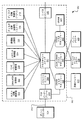
図1には、ローカルエリアネットワーク(LAN)102およびストレージエリアネットワーク(SAN)104を含む代表的なコンピュータ使用およびストレージフレームワーク100が例示されている。種々のアプリケーション顧客106が、LAN102を介してアプリケーションサーバー108へとネットワーク接続されている。アプリケーションサーバー108によって、アプリケーション顧客106は、アプリケーションサーバー108に常駐するアプリケーションへのアクセスが可能となる。そのようなアプリケーションは、1つ以上のアプリケーションデータストレージデバイス110に蓄積されるデータ(例えば、eメールデータベース)に依存する。したがって、SAN104は、アプリケーションサーバー108とアプリケーションデータストレージデバイス110との間の接続性を提供して、アプリケーションがデータにアクセスできるようにする。
FIG. 1 illustrates an exemplary computer usage and
SAN104には、冗長のため典型的には2つのインテリジェントストレージプロセッサー(ISP)を有するインテリジェントストレージプロセッサー基板を含む1つ以上のインテリジェントSANスイッチが含まれている。インテリジェントSANは、インターフェースストレージデバイス110を、SAN104における残りのSANスイッチファブリックに切り替える。各インテリジェントSANスイッチは、ハードウェア、ファームウェアおよび/またはアプリケーションソフトウェアの種々の組み合わせにおいて実施され、ISPおよび/または関連するプロセッサーによって実行されるルーティング、量管理、データ移動および複製のような分類されたストレージサービスを提供することができる。図1に示されるSAN104には、代表的な書き込みリファレンスメッシュ(WORM)を実行するISPを有するインテリジェントスイッチが含まれており、それは、後に続く図に関してより詳細に記述されるような洗練されたプログラミングモデルを支援する。
The SAN 104 includes one or more intelligent SAN switches that include an intelligent storage processor board that typically has two intelligent storage processors (ISPs) for redundancy. The intelligent SAN switches the
図2には、インテリジェントSANスイッチの代表的なインテリジェントストレージプロセッサー基板200のブロック図が例示されている。ISP基板200には、16ビット(またはそれ未満の)広域並列低電圧差動(LVD)バス206(「eバス」)によって結合される2つのISPサブシステム202および204が含まれている。ISPサブシステム202には、ISP208が含まれており、それには、1つのファイバーチャンネルホストリンク216と2つのファイバーチャンネルストレージリンク218へのインターフェースおよび、リアルタイムオペレーティングシステム(RTOS)を実行するポリシープロセッサー212が含まれている。ISP208およびポリシープロセッサー212は、PCIバス214を介して通信することができ、ISP208とポリシープロセッサー212は、双方ともメモリー222にアクセスできる。
FIG. 2 illustrates a block diagram of a typical intelligent
1つの実施例において、ISP208には、異なるカスタムロジックを備える7つの機能制御器コア(FCC)と3つのリストマネージャー(LM)特定用途プロセッサーとが含まれている。FCCおよびLMは、クロスポイントスイッチ(CPS)FCC‐LMメッセージクロスバーを介して通信する。そのように、FCCは、所定の条件に応じてCPSメッセージを生成し、これらのメッセージをメモリーモジュールにアクセスし、または所望のISP動作を呼び出すために、CPSを通してリストマネージャーへと送る。同様に、リストマネージャーからの応答は、CPSを介してFCCへと伝えられる。ポリシープロセッサーはまた、リストマネージャーと通信し、そしてCPSを用いてメモリーにアクセスする。また他の実施例も使用されることが理解されるべきである。 In one embodiment, the ISP 208 includes seven function controller cores (FCC) with different custom logic and three list manager (LM) application specific processors. The FCC and LM communicate via a crosspoint switch (CPS) FCC-LM message crossbar. As such, the FCC generates CPS messages in response to predetermined conditions and sends these messages through the CPS to the list manager to access the memory module or invoke the desired ISP operation. Similarly, the response from the list manager is communicated to the FCC via the CPS. The policy processor also communicates with the list manager and accesses memory using the CPS. It should be understood that other embodiments may also be used.
FCCは、特定の機能に基づいてカスタマイズされたロジックを実行することのできる特化されたプロセッサーである。FCCが含んでいるのは、高度に柔軟な特長の組み合わせと、リストマネージャーと通信するCPSメッセージを用いて、CPSを通してメモリーにアクセスする強力なインターフェースである。リストマネージャーは、ISP208とそのパートナーISP210、並びにポリシープロセッサー212のFCC用メモリーへのアクセスポイントとして動作することのできる特化されたメッセージプロセッサーである。リストマネージャーはまた、CPSを通して受け取られるメッセージに応答する他の特化された機能性を提供することもできる。受け取られたメッセージおよびデータは、リストマネージャーによって保持されアクセスされるリストに蓄積される。スケジューリングプロトコルにしたがって、リストマネージャーは、メッセージによって定義される動作を実行する。
An FCC is a specialized processor that can execute customized logic based on specific functions. The FCC includes a powerful interface that accesses memory through the CPS using a combination of highly flexible features and CPS messages that communicate with the list manager. The list manager is a specialized message processor that can act as an access point to the
ポリシープロセッサー212は、スイッチのベンダーがプログラムすることができ、「価値付加」機能性を提供する。すなわち、ポリシープロセッサー212は、カスタムロジックを実行し、ISP208を介して洗練された動作を行うことができる。多くの方法で、ポリシープロセッサー212は、FCCにいくぶん等しいようなISP208によって処理される。ポリシープロセッサー212は、いずれのリストマネージャーにもメッセージを送ることができ、かついずれのリストマネージャーからも、全てCPSを介して戻される応答を受け取ることができる。ISPによって発行されるメッセージの応答は、結果としてポリシープロセッサー212を中断するものとなり、それは、その中断に応答して、リストマネージャーの応答を得るようISPのレジスタを読むことができる。したがって、ポリシープロセッサー212はまた、メモリー222にアクセスし、CPSメッセージおよびリストマネージャーを用いてISP208内の動作をトリガーすることができる。
The
したがって、SANスイッチベンダは、ポリシープロセッサー212で実行されるカスタムストレージサービスアプリケーションを作り出すことができる。ストレージサービスアプリケーションは、例えば、付随オーバーヘッドでの個々のPCI読み取りまたは書き込みオペレーションを介してメモリーウインドウを開いてアクセスすることによって、ISPレジスタアクセスおよびPCIバス214の上のDMAを通してISP208の機能にアクセスできる。実施例によっては、個々のPCIアクセスよりも速いアクセスも支援する。例えば、前述のシステムの実施例においては、ポリシープロセッサーは、PCIバス214越しのキャッシュ書き込みを通してISPの機能にアクセスするパワーPCプロセッサーで実現される。ただし、他のプロセッサーやアクセス方法が使用されてもよい。
Accordingly, SAN switch vendors can create custom storage service applications that run on the
図3には、代表的なストレージシステム300の構成要素が例示されている。構成要素の中で、ISP302は、ポリシープロセッサー304、バッファメモリーモジュール306、キャッシュテーブルメモリー308および交換メモリーモジュール310と結合されている。したがって、ポリシープロセッサー304は、ストレージシステムのためのカスタムアプリケーションを実行して、PCIバス312およびISP302におけるPCIインターフェース313を介してISPの機能およびメモリーモジュールにおけるデータにアクセスできる。
FIG. 3 illustrates components of a
前述のシステム300の実施例において、ポリシープロセッサー304は、PCIバス312越しに32MBメモリーウインドウが備えられ、ISP302へのアクセスが可能となっている。ただし、代わりのサイズのメモリーウインドウも考えられる。例えば、代表的なポリシープロセッサーは、32バイトのキャッシュラインサイズを有し、単一の「バースト」動作としてキャッシュライン全体を強制的に発する機構を提供する。64ビットPCIインターフェースについて、これは、(調停および接続の後)結果としてアドレスサイクルを生じ、それに4つの64ビットデータワードサイクルが続く。
In the
1つの実施例において、ISP302には、7つのFCCが含まれている。これらのFCCのうち3つは、最初にファイバーチャンネルインターフェースに接続されている。これらのFCCの各々は、2つのDMAインターフェースを制御する。これらのFCCは、ホスト交換制御器314、ディスク交換制御器(コア1)316およびディスク交換制御器(コア2)318と名付けられる。残りの4つのFCCは、あるカスタムロジックを有するとともに、コマンドルーティング制御器320、DMA/XOR制御器322、メタデータ制御器324および雑機能制御器326といった一般的な目的の機能を提供する。
In one embodiment,
各FCCは、65,536個の16ビットレジスタのレジスタアドレススペース(128KB)を有する。このスペースの最初の4分の1(0xC000−0xFFFF)は、実際のFCCプログラミングインストラクションを含む書き込み可能な制御ストレージ(WCS)に確保されている。下位の512個の16ビットは、そのままのレジスタである。レジスタアドレススペースの残りは、カスタムロジックまたは一般の可変スペースへのアクセスを提供する。FCCは、CPS311およびリストマネージャーを介してメモリー306、308および310にアクセスすることができる。リストマネージャーを通してFCCは、リスト操作、リスト検索、フィールド抽出、フィールド挿入(蓄積)、フィールドコピー、フィールド増加、フィールド減少、フィールドビットセットおよびフィールドビットクリアを要求することができ、同様にリストマネージャーによって管理されるリストについての情報を要求する。
Each FCC has a register address space (128 KB) of 65,536 16-bit registers. The first quarter of this space (0xC000-0xFFFF) is reserved in a writable control storage (WCS) that contains the actual FCC programming instructions. The lower 512 16 bits are the registers as they are. The rest of the register address space provides access to custom logic or general variable space. The FCC can access the
リストマネージャーによって、FCCおよびポリシープロセッサー304には、メモリーモジュールへのアクセスが備えられる。バッファメモリーモジュール306は、ポリシープロセッサー304によって消費される実際のユーザーデータ、および幾分かの関連するメタデータを保持するためにあらかじめ確保されている。交換メモリーモジュール310は、バッファメモリーモジュール306においてバッファを記述するメタデータを保持する。キャッシュテーブルメモリーモジュール308もまた、メタデータを含むことができるが、別の特定の実施例においては、このメモリーモジュール308は使用されていない。SRAMモジュール333は、未決のコマンドのリストおよび現在進行中の状況に高速でアクセスするのに用いられる。結果的にDRAMリストマネージャー328は、交換メモリーモジュール308およびPCIインターフェース313へのアクセスを提供する。二重DRAMリストマネージャー330は、キャッシュテーブルメモリーモジュール308およびバッファメモリーモジュール306へのアクセスを提供する。SRAMリストマネージャー332は、SRAM333およびキャッシュテーブルメモリー308へのアクセスを提供する。
The list manager provides the FCC and
ISP302は、eバスインターフェース336を用いてパートナーISP(図示されていない)と通信する。オペレーションコードおよび/またはデータを含むメッセージが、リストマネージャーによってCPS311を通してeバスインターフェース336に送られ、それは、そのメッセージを、パートナーISPのeバスインターフェースに送る。同様に、所定のISPのFCCおよびポリシープロセッサーは、ISP302のCPS311を通して、メッセージをeバスインターフェース336へと送ることができ、それによって、ISP302のFCCおよびポリシープロセッサーが、パートナーISPのリストマネージャーとコマンドおよびデータの通信を行えるようにする。
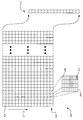
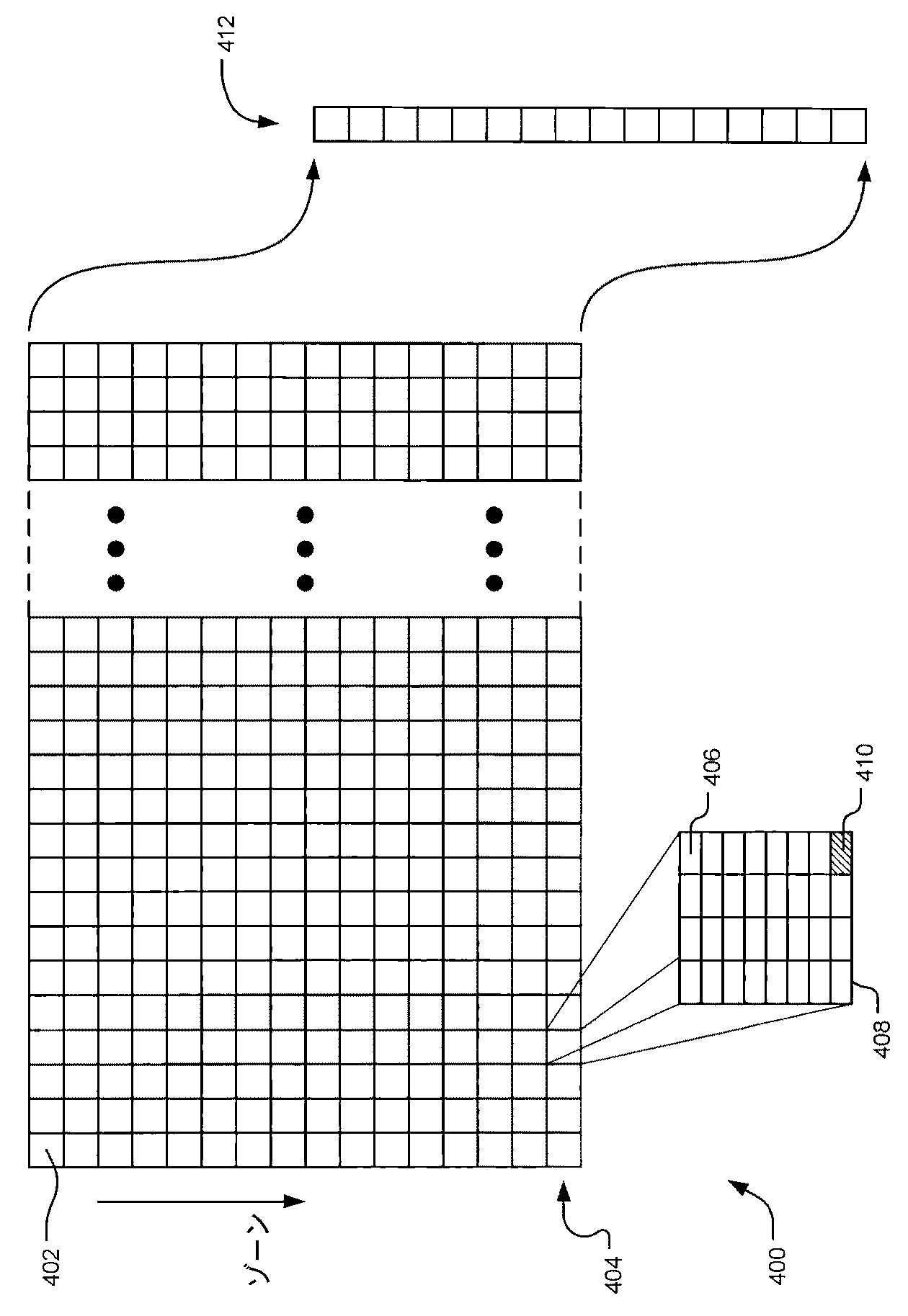
図4には、代表的な書き込みリファレンスメッシュ400が例示されている。1つの実施例において、64MBメモリーウインドウ(26ビットメモリーアドレス)が、ISPのベースアドレスレジスタ(図示されていない)によって定義されている。ウインドウの下位32MBは、キャッシュテーブルメモリーモジュールおよび交換メモリーモジュールのような、ストレージエンジンと関連する他のメモリーへのアクセスを可能とする。メモリーウインドウの上位32MBは、CPSアクセス領域(CAR)と呼ばれ、それを通してポリシープロセッサーは、ISPメモリーおよび機能にアクセスすることができる。代表的な実施例において、代表的なメモリーウインドウにおけるアドレスの下位25ビットは、以下のように定義される。
メッシュインデックスは、アドレシングについて無視される(ただし、それは後で、CPSメッセージの「タグ」として用いられる)。そうであるので、ポリシープロセッサーがメモリーウインドウのCARに書き込むとき、25ビットアドレスは、PCIインターフェースにおける超高速メモリーアクセスとして実行される実際の32バイトのみをアドレスするよう縮小する。そのようなアクセスは、32バイトバースト読み取りまたは32バイトバースト書き込みとして行われるが、4バイト(32ビット)単一ロングワードアクセスおよび単一バイトアクセスもまた実行される。 The mesh index is ignored for addressing (although it is later used as a “tag” in the CPS message). As such, when the policy processor writes to the CAR of the memory window, the 25-bit address is reduced to address only the actual 32 bytes that are executed as a very fast memory access at the PCI interface. Such accesses are made as 32-byte burst reads or 32-byte burst writes, but 4-byte (32-bit) single longword accesses and single-byte accesses are also performed.
メッシュ400には、ゾーン404に配置される複数の配列されたメッシュエントリー402が含まれており、それらは、メモリーウインドウを通してポリシープロセッサーによってアクセス可能である。1つの実施例において、メッシュは、2MB境界で16のゾーンに分割される。ただし、他の構成も考えられる。したがって、ポリシープロセッサーは、データパケット(例えば、1つの実施例におけるデータの32バイト)を、メモリーウインドウを通してメッシュ400における個々のメッシュエントリーに書き込むことができ、ここでデータの各バイトは、メッシュエントリーにおける個々のアドレス位置に書き込まれる。
したがって、メッシュ400の各メッシュエントリー402には、拡大されたフレーム408に示されるように、複数のアドレス位置406が含まれている。リファレンス位置410が、各メッシュエントリーにおいて指定されて特定のアクションをトリガーする。リファレンス位置への書き込みの検出は、「リファレンス」を表し、それは、書き込まれたセルエントリーが位置するゾーンと特に関連するアクションをトリガーするイベントである。
Thus, each
一般に、書き込みリファレンスメッシュは、メッシュにおける個々のメッシュエントリーのリファレンス位置へのメモリー書き込みオペレーションの検出に応答して、ISPにおける特定のアクションをトリガーする書き込み感応メモリーウインドウを実現する。代表的な実施例において、リファレンス位置への書き込みオペレーションもまた、結果として「タグ」を生成し、それは、メモリー書き込みオペレーションにおいて用いられるメモリーアドレスのメッシュインデックス部分から得られる。 In general, the write reference mesh implements a write sensitive memory window that triggers a specific action in the ISP in response to detecting a memory write operation to the reference location of an individual mesh entry in the mesh. In an exemplary embodiment, a write operation to a reference location also results in a “tag” that is obtained from the mesh index portion of the memory address used in the memory write operation.
例えば、メッシュエントリーにおける書き込み感応性は、以下のように実現される。
(1)If(Address&Mask1)==Matchであるならば、メッシュエントリーにおけるリファレンス位置への書き込みが検出される。
(2)Tag=(Address&Mask2)>>5
ここで、AddressはPCI書き込みオペレーションからの書き込みアドレスを表し、Mask1は、バイトオフセットを含まないアドレスビット位置においてクリアであり(例えば、Mask1=0x0000001F)、Mask2は、メッシュインデックスを含むアドレスビット位置においてセットであり(例えば、Mask2=0x001FFFE0)、Matchは、所定のゾーンの所定のメッシュエントリー内のリファレンス位置を表し(例えば、0x0000001F)、シフトは、メッシュインデックスをレジスタの下位ビットに移すのに必要とされるビット数を表す(例えば、表1において与えられる代表的な25ビットアドレスの例においてシフト=5)。この検出ロジックは、リファレンス位置が複数バイト書き込みオペレーションに含まれているとき作用する。したがって、メッシュエントリーにおけるリファレンス位置への書き込みが検出されるならば、書き込みアドレスのメッシュインデックス部分からタグが作り出される。
For example, the writing sensitivity in the mesh entry is realized as follows.
(1) If If (Address & Mask1) == Match, writing to the reference position in the mesh entry is detected.
(2) Tag = (Address & Mask2) >> 5
Here, Address represents the write address from the PCI write operation, Mask1 is clear at the address bit position not including the byte offset (for example, Mask1 = 0x0000001F), and Mask2 is set at the address bit position including the mesh index. (Eg, Mask2 = 0x001FFFE0), Match represents the reference position within a given mesh entry for a given zone (eg, 0x0000001F), and a shift is required to move the mesh index to the low order bits of the register (For example, shift = 5 in the typical 25-bit address example given in Table 1). This detection logic works when the reference location is included in a multibyte write operation. Thus, if a write to a reference location in a mesh entry is detected, a tag is created from the mesh index portion of the write address.
各ゾーンについて、ISPは、32ビットレジスタおよびゾーンテンプレートレジスタ412と呼ばれる6つの16ビットレジスタを支援する。各32ビットレジスタは、ゾーンパケットビットマスクレジスタと呼ばれ、以下のように定義される。
パケットテンプレートレジスタと呼ばれる6つの16ビットレジスタは、以下のように定義される。
上に定義される6つのレジスタとポリシープロセッサーによって書き込まれる16のデータワード(すなわち、32バイトパケット)の組み合わせは、22個の16ビットレジスタのアレイとして取り扱うことができる。リファレンス位置への書き込みが検出されるならば、タグ値が、対応するゾーンのパケットテンプレートレジスタのタグフィールドに書き込まれる。パケットテンプレートレジスタの他のフィールドは、各ゾーンについて、ポリシープロセッサーによって予め定義されている。 The combination of the six registers defined above and the 16 data words (ie, 32-byte packets) written by the policy processor can be treated as an array of 22 16-bit registers. If writing to the reference location is detected, the tag value is written to the tag field of the packet template register of the corresponding zone. Other fields in the packet template register are predefined by the policy processor for each zone.
対応するゾーンテンプレートレジスタのスキャター‐ギャザーマスクによって、これら22個のレジスタのいずれが、自動的に生成されるCPSメッセージを構築するのに用いられるのかが定義される。例えば、スキャター‐ギャザーマスクが「000003F」を含むならば、ヘッダー、オペレーション、タグおよび固定パラメータフィールド0、1および2のみが、CPSパケットを構築するのに用いられる。反対に、スキャター‐ギャザーマスクが「00001FF」を含むならば、ヘッダー、オペレーション、タグ、固定パラメータフィールド0、1および2並びにデータワード0‐2が、CPSパケットを構築するのに用いられる。
The scatter-gather mask of the corresponding zone template register defines which of these 22 registers is used to construct the automatically generated CPS message. For example, if the scatter-gather mask contains “000003F”, only the header, operation, tag and fixed
CPSパケットの生成は、ゾーンテンプレートレジスタ内のフラグビットおよびデータワード0のビット15に関する設定次第である(ポリシープロセッサーによってメッシュエントリーに書き込まれる)。フラッグがクリアであるならば、リファレンスが検出されるとき、CPSパケットは自動的に生成される。また、フラッグが設定されかつデータワード0のビット15が設定されるならば、リファレンスが検出されるとき、CPSパケットが自動的に生成される。しかしながら、フラッグが設定されかつデータワード0のビット15がクリアであるならば、リファレンスが検出されるとき、CPSパケットは自動的に生成されない。CPSパケットの生成をこのように条件を付けてトリガーすることで、32バイトデータバケットの全体に満たないものがポリシープロセッサーキャッシュから消去されるとき、アクションの生成(すなわちCPSパケットの生成)が防止される。 The generation of the CPS packet depends on the setting of the flag bit in the zone template register and bit 15 of data word 0 (written to the mesh entry by the policy processor). If the flag is clear, a CPS packet is automatically generated when a reference is detected. Also, if the flag is set and bit 15 of data word 0 is set, a CPS packet is automatically generated when a reference is detected. However, if the flag is set and bit 15 of data word 0 is clear, the CPS packet is not automatically generated when the reference is detected. This conditional triggering of CPS packet generation prevents action generation (ie, CPS packet generation) when less than the entire 32-byte data bucket is purged from the policy processor cache. The
前述のように、リストマネージャーは、特化されたメッセージプロセッサーである。したがって、リストマネージャーは、ISPまたはそのパートナーISP内のアクションを結果として生じるオペレーションコードの組を支援する。代表的なコードには、「読み取り/書き込み連続メモリー位置」(読み取りシーケンス/書き込みシーケンス)、「読み取り/書き込みランダムメモリー位置」(読み取りランダム/書き込みランダム)、「補充テーブル」、「ゲットリストヘッド/テール」(ゲットヘッド/ゲットテール)、「増加/減少フィールド」(増加フィールド/減少フィールド)、「書き込みエントリーデータ」、「ポストエントリーデータ」「アンリンクおよび読み取りシーケンス」、「アンリンクおよび読み取りランダム」、「書き込みシーケンスおよびポスト」、「書き込みリング」、「書き込みリングおよび通知」、「読み取りリング」のようなオペレーションが無制限に含まれる。これらの代表的なオペレーションコードによって表されるアクションを通して、メモリーをアクセスすることができ、FCCによる処理のためにメッセージを列に並べる(すなわち、「ポストする」)ことができ、かつPCIデバイス(例えば、パートナーISP)に、処理される新しいリストエントリー(例えば、メッセージ)について通知することができる。 As mentioned above, the list manager is a specialized message processor. Thus, the list manager supports a set of operation codes that result in an action in the ISP or its partner ISP. Typical codes include "read / write continuous memory position" (read sequence / write sequence), "read / write random memory position" (read random / write random), "replenishment table", "get list head / tail ”(Get head / get tail),“ increase / decrease field ”(increase field / decrease field),“ write entry data ”,“ post entry data ”,“ unlink and read sequence ”,“ unlink and read random ”, Unlimited operations such as “write sequence and post”, “write ring”, “write ring and notification”, “read ring” are included. Through actions represented by these representative operation codes, memory can be accessed, messages can be queued (ie, “posted”) for processing by the FCC, and PCI devices (eg, , The partner ISP) can be informed about new list entries (eg, messages) to be processed.
ヘッダーフィールドは、CPSパケットを特定のリストマネージャーに向けるルーティング情報を含む。そのように、所定のゾーンと関連するパケットテンプレートレジスタは、特定の結果を達成するために特定のアクションをトリガーする特定のリストマネージャーに向けてのパケットを定義できる。オプコードフィールドは、リストマネージャーが処理するオペレーションコードを含み、リストマネージャーによって受け取られるCPSメッセージと関連するアクションを表す。他のフィールドは、関連するアクションに有用なデータを含むことができる。例えば、リストフィールド、タグフィールドおよびその他のレジスタフィールドのいずれでも、どのリストがアクセスされ、どのデータが通信されるのかなどの影響を及ぼす。代表的なアクションが以下に記述される。 The header field contains routing information that directs the CPS packet to a particular list manager. As such, the packet template register associated with a given zone can define packets for a specific list manager that triggers a specific action to achieve a specific result. The opcode field contains the operation code that the list manager processes and represents the action associated with the CPS message received by the list manager. Other fields can contain data useful for the associated action. For example, any of the list field, tag field, and other register fields affects which list is accessed and which data is communicated. Representative actions are described below.
1つの実施例において、双方のパートナーISPでメタデータをミラー化することは冗長の目的で重要であり得るが、そのミラー化は、異なるISPサブシステム内の異なるアドレスで行われる。このシナリオにおいて、リファレンスに応答してトリガーするアクションは、eバスを横切ってのパートナーISPへのデータの書き込みオペレーションである。 In one embodiment, mirroring metadata at both partner ISPs may be important for redundancy purposes, but the mirroring is done at different addresses in different ISP subsystems. In this scenario, the action that triggers in response to the reference is a write operation of data to the partner ISP across the e-bus.
したがって、「データ転送ゾーン」と呼ばれるゾーンが、この機能のために取り分けられて「データ転送ウインドウ」を定義する。データ転送ゾーンのパケットテンプレートレジスタには、CPSを通って特定のリストマネージャーへとパケットを経路付けるヘッダーフィールドが含まれている。オペレーションフィールドエントリーには、書き込みエントリーデータが含まれており、リストフィールドエントリーは、パートナーISPのメモリーにおいて対応するメモリー範囲を参照するテーブルを参照する。 Thus, zones called “data transfer zones” are reserved for this function to define a “data transfer window”. The packet template register in the data transfer zone includes a header field that routes the packet through the CPS to a specific list manager. The operation field entry includes write entry data, and the list field entry refers to a table that refers to a corresponding memory range in the memory of the partner ISP.
例えば、データ転送ゾーンにおけるメッシュエントリーのリファレンス位置へのポリシープロセッサーによる書き込みオペレーションは、第一のISPにおいて検出される。それに応答して、CPSメッセージが自動的に生成され、パートナーISPのリストマネージャーに経路付けられる。CPSメッセージには、パートナーISPにおけるミラー化書き込みについて適当なメモリー範囲を参照するリストフィールドが含まれている。リストマネージャーがCPSメッセージのオプコードを実行するとき、第一のISPに書き込まれるデータは、パートナーISPのメモリーに書き込まれる。 For example, a write operation by the policy processor to the mesh entry reference location in the data transfer zone is detected at the first ISP. In response, a CPS message is automatically generated and routed to the list manager of the partner ISP. The CPS message includes a list field that references the appropriate memory range for mirrored writes at the partner ISP. When the list manager executes the CPS message opcode, the data written to the first ISP is written to the memory of the partner ISP.
第二の実施例において、要求および応答メッセージがISPパートナー間で迅速に送られ、例えば、ファイバーチャンネルプロトコル交換またはSCSI交換を実行する。このシナリオにおいてリファレンスに応答してトリガーされるアクションは、要求または応答をeバス越しにパートナーISPのメッセージリングバッファに送るものである。 In a second embodiment, request and response messages are sent quickly between ISP partners to perform, for example, a Fiber Channel protocol exchange or a SCSI exchange. The action triggered in response to the reference in this scenario is to send a request or response over the e-bus to the partner ISP's message ring buffer.
「メッセージ転送ゾーン」と呼ばれるゾーンが、この機能のために取り分けられている。メッセージ転送ゾーンのパケットテンプレートレジスタには、CPSを通して特定のリストマネージャーへとパケットを経路付けるヘッダーフィールドが含まれている。オプコードフィールドエントリーには、書き込みリングおよび通知オプコードと、メッセージについて適切なリングを識別するリングフィールドエントリーとが含まれている。 Zones called “message transfer zones” are reserved for this function. The packet template register in the message transfer zone includes a header field that routes the packet through the CPS to a specific list manager. The opcode field entry includes a write ring and notification opcode and a ring field entry that identifies the appropriate ring for the message.
例えば、パートナーISPのメッセージリングバッファへの書き込みオペレーションが、ポリシープロセッサーのISPのメッセージ転送ゾーンへの書き込みにより、ポリシープロセッサーによって呼び出される。メッセージ転送ゾーンにおけるメッシュエントリーのリファレンス位置への書き込みが検出されるとき、CPSメッセージが自動的に生成され、パートナーISPのリストマネージャーへと経路付けられる。CPSメッセージには、パートナーISPの適切なメッセージリングを参照するフィールドが含まれている。パートナーISPのリストマネージャーがCPSメッセージのオプコードを実行するとき、そのメッセージは、パートナーISPによってアクセスの可能なメモリーにおけるリングバッファに書き込まれる。 For example, a write operation to the message ring buffer of the partner ISP is invoked by the policy processor by writing to the message transfer zone of the policy processor ISP. A CPS message is automatically generated and routed to the list manager of the partner ISP when a write to the reference location of the mesh entry in the message transfer zone is detected. The CPS message includes a field that refers to the appropriate message ring of the partner ISP. When the partner ISP's list manager executes the CPS message opcode, the message is written to a ring buffer in memory accessible by the partner ISP.
図5には、書き込みリファレンスメッシュを使用する代表的なストレージシステムにおける論理オペレーションが例示されている。ウインドウ化オペレーション502によって、PCIメモリーウインドウのようなメモリーウインドウの書き込みリファレンスメッシュが定義される。ある実施例において、メッシュは64MBごとに配列されるが、他の配列も考えられる。メッシュには、ゾーンに組織されるメッシュエントリーが含まれている。各ゾーンは、それと関連するゾーンテンプレートレジスタを有しており、それによって、リファレンス位置への書き込みがゾーン内で検出されるときにトリガーされるアクションが定義される。
FIG. 5 illustrates logical operations in a typical storage system that uses a write reference mesh.
検出オペレーション504は、書き込みリファレンスメッシュにおけるメッシュエントリーのリファレンス位置への書き込みオペレーションを検出する。代表的な検出オペレーションが、回路ロジックとマスクおよびマッチ値を用いて先に記述されている。ただし、他の検出オペレーションも考えられる。いくつかの実施例において、タグ値もまた、検出オペレーション504で決定され、ゾーンテンプレートレジスタの1つにローディングされる。
A detect
メッセージングオペレーション506は、(ヘッダーフィールドにおける)オペレーションコードおよび経路付け情報の含まれるCPSメッセージを構築する。16ビットゾーンテンプレートレジスタおよび書き込みオペレーションのデータは、32ビットゾーンテンプレートレジスタのスキャター‐ギャザーマスクによってマスクされて、この構築に用いられる。そうして、関連するスキャター‐ギャザーマスクによって選択され、ポリシープロセッサーによって書き込まれる32バイトのデータとメッシュエントリーの位置するゾーンの16ビットゾーンテンプレートレジスタのフィールドがメッセージパケットにコピーされる。
経路付けオペレーション508は、構築されたメッセージパケットを、そのメッセージパケットのヘッダーフィールドの経路付け情報において識別されるリストマネージャーに送る。代わりに、そのメッセージは、サブシステム内のカスタムロジックの他の部分へと送られることもあり得る。いくつかの実施例において、リストマネージャーはローカルISPか、パートナーISPかその他のロジックにある。メッセージパケットは、ストレージエンジンによってCPSスイッチを通ってその目的地へと送られる。したがって、その経路付けはCPSスイッチによって行われる。
処理オペレーション510は、オプコードおよびメッセージパケットにおける他のフィールドによって特定されるオペレーションを実行する。リストマネージャーは、洗練されたメッセージプロセッサーであるので、そのようなオペレーションは相当に多様である。いくつかの代表的なオペレーションがここに記述されているが、しかしリストマネージャーは広く多様なオペレーションを行うように構築されていて、これらの例によって制限されるべきではない。
ここに記述されている本発明の実施例は、1つ以上のコンピュータシステムにおいて論理ステップとして実現されている。本発明の論理オペレーションは、(1)1つ以上のコンピュータシステムにおいてプロセッサーに実行される一連のステップとしておよび(2)1つ以上のコンピュータシステム内の相互接続されたマシーンまたは回路モジュールとして実現される。実施例は、発明を実施するコンピュータシステムの性能要件に依存する選択事項である。したがって、ここに記述される発明の実施例を構成する論理オペレーションは、オペレーション、ステップ、オブジェクトまたはモジュールとして多様に言及される。さらには、論理オペレーションは、特許請求の範囲に明確に順番が記述されているか、特定の順番が特許請求の範囲の記述によって固有に必要とされていない限り、どのような順番で行われてもよいことを理解すべきである。 The embodiments of the invention described herein are implemented as logical steps in one or more computer systems. The logical operations of the present invention are implemented as (1) a series of steps executed by a processor in one or more computer systems and (2) as interconnected machines or circuit modules in one or more computer systems. . The embodiment is a choice that depends on the performance requirements of the computer system implementing the invention. Accordingly, the logical operations making up the embodiments of the invention described herein are referred to variously as operations, steps, objects, or modules. In addition, logical operations may be performed in any order, unless explicitly stated in the claims or a specific order is specifically required by a claim statement. It should be understood.
上記明細書、例およびデータは、発明の代表的な実施例の構造および使用を完全に記述するものである。発明の精神および範囲から逸脱することなく多くの実施例を作ることができるので、発明は、添付される特許請求の範囲に存する。とりわけ、記述された技術は、ストレージシステムとは独立に使用してもよいことを理解すべきである。したがって他の実施例も考えられる。 The above specification, examples and data provide a complete description of the structure and use of exemplary embodiments of the invention. Since many embodiments can be made without departing from the spirit and scope of the invention, the invention resides in the claims hereinafter appended. In particular, it should be understood that the described techniques may be used independently of the storage system. Other embodiments are therefore conceivable.
100 ストレージフレームワーク
102 ローカルエリアネットワーク
104 ストレージエリアネットワーク
106 アプリケーション顧客
108 アプリケーションサーバー
110 アプリケーションデータストレージデバイス
200 インテリジェントストレージプロセッサー(ISP)基板
202,204 ISPサブシステム
206 広域並列低電圧差動(LVD)バス(eバス)
208,210 インテリジェントストレージプロセッサー
212 ポリシープロセッサー
214 PCIバス
216 ファイバーチャンネルホストリンク
218 ファイバーチャンネルストレージリンク
300 ストレージシステム
302 ISP
304 ポリシープロセッサー
306 バッファメモリー
308 キャッシュテーブルメモリー
310 交換メモリー
312 PCIバス
314 ホスト交換制御器
316 ディスク交換制御器(コア1)
318 ディスク交換制御器(コア2)
320 Cmdルーティング制御器
322 DMA/XOR制御器
324 メタデータ制御器
326 雑機能制御器
328 DRAMリストマネージャー
330 DUAL−DRAMリストマネージャー
332 SRAMリストマネージャー
333 SRAM
334 ストレージエンジン
336 Eバスインターフェース
400 リファレンスメッシュ
402 メッシュエントリー
404 ゾーン
412 ゾーンテンプレートレジスタ
100
208, 210
304
318 Disk exchange controller (core 2)
320
334 Storage engine 336
Claims (20)
メッシュエントリーのリファレンス位置への書き込みオペレーションを検出し、
検出オペレーションに応答して、書き込まれたメッシュエントリーと関連するアクションをトリガーする、
ステップを含む、書き込みリファレンスメッシュを構成する方法。 Defining a memory window mesh comprising an array of mesh entries each having a plurality of address locations including an address location designated as a reference location;
Detects a write operation to the mesh entry reference position,
In response to a detect operation, trigger an action associated with the written mesh entry,
A method of constructing a writing reference mesh including steps.
書き込まれたメッシュエントリーと関連するアクションを、メッシュエントリーのリファレンス位置への書き込みオペレーションの検出に応答してトリガーするストレージエンジンと
を備える書き込みリファレンスメッシュを構成するシステム。 A memory window mesh including an array of mesh entries, each mesh entry including a plurality of address positions, the mesh entry including a memory window mesh including an address position designated as a reference position;
A system for constructing a write reference mesh comprising a storage engine that triggers an action associated with the written mesh entry in response to detection of a write operation to the reference location of the mesh entry.
Applications Claiming Priority (1)
| Application Number | Priority Date | Filing Date | Title |
|---|---|---|---|
| US11/042,424 US7287128B1 (en) | 2005-01-25 | 2005-01-25 | Write on reference mesh |
Publications (2)
| Publication Number | Publication Date |
|---|---|
| JP2006209727A true JP2006209727A (en) | 2006-08-10 |
| JP4679963B2 JP4679963B2 (en) | 2011-05-11 |
Family
ID=36966468
Family Applications (1)
| Application Number | Title | Priority Date | Filing Date |
|---|---|---|---|
| JP2005142907A Expired - Fee Related JP4679963B2 (en) | 2005-01-25 | 2005-05-16 | Method and system for constructing a writing reference mesh |
Country Status (2)
| Country | Link |
|---|---|
| US (1) | US7287128B1 (en) |
| JP (1) | JP4679963B2 (en) |
Families Citing this family (1)
| Publication number | Priority date | Publication date | Assignee | Title |
|---|---|---|---|---|
| US8914540B1 (en) * | 2008-07-01 | 2014-12-16 | Cisco Technology, Inc. | Multi-fabric SAN based data migration |
Citations (3)
| Publication number | Priority date | Publication date | Assignee | Title |
|---|---|---|---|---|
| JPH06247010A (en) * | 1993-02-25 | 1994-09-06 | Oki Electric Ind Co Ltd | Command processor in printer |
| JPH0772988A (en) * | 1993-09-06 | 1995-03-17 | Seiko Epson Corp | Information equipment |
| JP2004523831A (en) * | 2001-02-13 | 2004-08-05 | キャンデラ, インコーポレイテッド | Silicon-based storage virtualization server |
Family Cites Families (10)
| Publication number | Priority date | Publication date | Assignee | Title |
|---|---|---|---|---|
| US5377344A (en) | 1991-07-31 | 1994-12-27 | Toyo Corporation | Selective memory transaction monitor system |
| US6442585B1 (en) | 1997-11-26 | 2002-08-27 | Compaq Computer Corporation | Method for scheduling contexts based on statistics of memory system interactions in a computer system |
| US6202127B1 (en) | 1997-11-26 | 2001-03-13 | Compaq Computer Corporation | Apparatus for spatial and temporal sampling in a computer memory system |
| US6601149B1 (en) | 1999-12-14 | 2003-07-29 | International Business Machines Corporation | Memory transaction monitoring system and user interface |
| US6742101B2 (en) | 2001-06-29 | 2004-05-25 | Fujitsu Limited | Scalable and flexible method for address space decoding in a multiple node computer system |
| US6862634B2 (en) | 2001-06-29 | 2005-03-01 | Fujitsu Limited | Mechanism to improve performance in a multi-node computer system |
| US7213081B2 (en) | 2001-06-29 | 2007-05-01 | Fujitsu Limited | Dynamic determination of memory mapped input output range granularity for multi-node computer system |
| US6970809B2 (en) | 2001-08-29 | 2005-11-29 | International Business Machines Corporation | Automated configuration of on-circuit facilities |
| US7120728B2 (en) * | 2002-07-31 | 2006-10-10 | Brocade Communications Systems, Inc. | Hardware-based translating virtualization switch |
| US7334077B2 (en) * | 2003-10-17 | 2008-02-19 | Renesas Technology America, Inc. | Method and apparatus for smart memory pass-through communication |
-
2005
- 2005-01-25 US US11/042,424 patent/US7287128B1/en not_active Expired - Fee Related
- 2005-05-16 JP JP2005142907A patent/JP4679963B2/en not_active Expired - Fee Related
Patent Citations (3)
| Publication number | Priority date | Publication date | Assignee | Title |
|---|---|---|---|---|
| JPH06247010A (en) * | 1993-02-25 | 1994-09-06 | Oki Electric Ind Co Ltd | Command processor in printer |
| JPH0772988A (en) * | 1993-09-06 | 1995-03-17 | Seiko Epson Corp | Information equipment |
| JP2004523831A (en) * | 2001-02-13 | 2004-08-05 | キャンデラ, インコーポレイテッド | Silicon-based storage virtualization server |
Also Published As
| Publication number | Publication date |
|---|---|
| JP4679963B2 (en) | 2011-05-11 |
| US7287128B1 (en) | 2007-10-23 |
Similar Documents
| Publication | Publication Date | Title |
|---|---|---|
| EP1606712B1 (en) | System and method for dynamic mirror-bank addressing | |
| US11048569B1 (en) | Adaptive timeout mechanism | |
| USRE44610E1 (en) | Node identification for distributed shared memory system | |
| US7562176B2 (en) | Apparatus and methods for clustering multiple independent PCI express hierarchies | |
| US7496698B2 (en) | System and method for efficient implementation of a shared receive queue | |
| US10846163B1 (en) | Hybrid hardware and software reporting management | |
| US10762137B1 (en) | Page table search engine | |
| WO2022007644A1 (en) | Multiprocessor system and method for configuring multiprocessor system | |
| KR101575070B1 (en) | Apparatus, system and method for providing access to a device function | |
| US10810133B1 (en) | Address translation and address translation memory for storage class memory | |
| KR102792263B1 (en) | Memory card and method for processing data using the card | |
| CN117827449B (en) | Server physical memory expansion architecture, servers, methods, devices, and media | |
| KR102964796B1 (en) | Memory tiering techniques in computing systems | |
| JP7856240B2 (en) | Memory operation management in computing systems | |
| US10437750B2 (en) | Relative data width indication for read responses routed by an interconnect | |
| US20060277350A1 (en) | Stripe buffer list | |
| BR112016003488B1 (en) | STORAGE SYSTEM, METHOD, AND APPARATUS FOR PROCESSING OPERATION REQUEST | |
| JP4679963B2 (en) | Method and system for constructing a writing reference mesh | |
| US10754789B1 (en) | Address translation for storage class memory in a system that includes virtual machines | |
| CN110945843A (en) | Virtual switching apparatus and method | |
| US10402329B1 (en) | Reducing traffic in hierarchical cache interconnects | |
| JP4446961B2 (en) | Integrated circuit and method for sending requests | |
| KR20230116887A (en) | Tags for request packets on network communication links | |
| US7424496B1 (en) | Asymmetric coherency protection | |
| CN102236572B (en) | Firmware loading method and equipment |
Legal Events
| Date | Code | Title | Description |
|---|---|---|---|
| A621 | Written request for application examination |
Free format text: JAPANESE INTERMEDIATE CODE: A621 Effective date: 20080512 |
|
| RD03 | Notification of appointment of power of attorney |
Free format text: JAPANESE INTERMEDIATE CODE: A7423 Effective date: 20100526 |
|
| A977 | Report on retrieval |
Free format text: JAPANESE INTERMEDIATE CODE: A971007 Effective date: 20101228 |
|
| TRDD | Decision of grant or rejection written | ||
| A01 | Written decision to grant a patent or to grant a registration (utility model) |
Free format text: JAPANESE INTERMEDIATE CODE: A01 Effective date: 20110118 |
|
| A01 | Written decision to grant a patent or to grant a registration (utility model) |
Free format text: JAPANESE INTERMEDIATE CODE: A01 |
|
| A61 | First payment of annual fees (during grant procedure) |
Free format text: JAPANESE INTERMEDIATE CODE: A61 Effective date: 20110202 |
|
| R150 | Certificate of patent or registration of utility model |
Free format text: JAPANESE INTERMEDIATE CODE: R150 |
|
| FPAY | Renewal fee payment (event date is renewal date of database) |
Free format text: PAYMENT UNTIL: 20140210 Year of fee payment: 3 |
|
| R250 | Receipt of annual fees |
Free format text: JAPANESE INTERMEDIATE CODE: R250 |
|
| R250 | Receipt of annual fees |
Free format text: JAPANESE INTERMEDIATE CODE: R250 |
|
| LAPS | Cancellation because of no payment of annual fees |