JP2006209727A - 書き込みリファレンスメッシュを構成する方法およびシステム - Google Patents
書き込みリファレンスメッシュを構成する方法およびシステム Download PDFInfo
- Publication number
- JP2006209727A JP2006209727A JP2005142907A JP2005142907A JP2006209727A JP 2006209727 A JP2006209727 A JP 2006209727A JP 2005142907 A JP2005142907 A JP 2005142907A JP 2005142907 A JP2005142907 A JP 2005142907A JP 2006209727 A JP2006209727 A JP 2006209727A
- Authority
- JP
- Japan
- Prior art keywords
- mesh
- memory
- entry
- address
- action
- Prior art date
- Legal status (The legal status is an assumption and is not a legal conclusion. Google has not performed a legal analysis and makes no representation as to the accuracy of the status listed.)
- Granted
Links
Images



Classifications
-
- G—PHYSICS
- G06—COMPUTING OR CALCULATING; COUNTING
- G06F—ELECTRIC DIGITAL DATA PROCESSING
- G06F13/00—Interconnection of, or transfer of information or other signals between, memories, input/output devices or central processing units
- G06F13/38—Information transfer, e.g. on bus
- G06F13/40—Bus structure
- G06F13/4004—Coupling between buses
- G06F13/4022—Coupling between buses using switching circuits, e.g. switching matrix, connection or expansion network
-
- G—PHYSICS
- G06—COMPUTING OR CALCULATING; COUNTING
- G06F—ELECTRIC DIGITAL DATA PROCESSING
- G06F3/00—Input arrangements for transferring data to be processed into a form capable of being handled by the computer; Output arrangements for transferring data from processing unit to output unit, e.g. interface arrangements
- G06F3/06—Digital input from, or digital output to, record carriers, e.g. RAID, emulated record carriers or networked record carriers
- G06F3/0601—Interfaces specially adapted for storage systems
- G06F3/0602—Interfaces specially adapted for storage systems specifically adapted to achieve a particular effect
- G06F3/061—Improving I/O performance
-
- G—PHYSICS
- G06—COMPUTING OR CALCULATING; COUNTING
- G06F—ELECTRIC DIGITAL DATA PROCESSING
- G06F3/00—Input arrangements for transferring data to be processed into a form capable of being handled by the computer; Output arrangements for transferring data from processing unit to output unit, e.g. interface arrangements
- G06F3/06—Digital input from, or digital output to, record carriers, e.g. RAID, emulated record carriers or networked record carriers
- G06F3/0601—Interfaces specially adapted for storage systems
- G06F3/0628—Interfaces specially adapted for storage systems making use of a particular technique
- G06F3/0655—Vertical data movement, i.e. input-output transfer; data movement between one or more hosts and one or more storage devices
- G06F3/0659—Command handling arrangements, e.g. command buffers, queues, command scheduling
-
- G—PHYSICS
- G06—COMPUTING OR CALCULATING; COUNTING
- G06F—ELECTRIC DIGITAL DATA PROCESSING
- G06F3/00—Input arrangements for transferring data to be processed into a form capable of being handled by the computer; Output arrangements for transferring data from processing unit to output unit, e.g. interface arrangements
- G06F3/06—Digital input from, or digital output to, record carriers, e.g. RAID, emulated record carriers or networked record carriers
- G06F3/0601—Interfaces specially adapted for storage systems
- G06F3/0668—Interfaces specially adapted for storage systems adopting a particular infrastructure
- G06F3/0671—In-line storage system
- G06F3/0683—Plurality of storage devices
-
- G—PHYSICS
- G06—COMPUTING OR CALCULATING; COUNTING
- G06F—ELECTRIC DIGITAL DATA PROCESSING
- G06F12/00—Accessing, addressing or allocating within memory systems or architectures
- G06F12/02—Addressing or allocation; Relocation
- G06F12/08—Addressing or allocation; Relocation in hierarchically structured memory systems, e.g. virtual memory systems
- G06F12/0802—Addressing of a memory level in which the access to the desired data or data block requires associative addressing means, e.g. caches
- G06F12/0877—Cache access modes
- G06F12/0879—Burst mode
Landscapes
- Engineering & Computer Science (AREA)
- Theoretical Computer Science (AREA)
- Physics & Mathematics (AREA)
- General Engineering & Computer Science (AREA)
- General Physics & Mathematics (AREA)
- Human Computer Interaction (AREA)
- Mathematical Physics (AREA)
- Computer Hardware Design (AREA)
- Information Retrieval, Db Structures And Fs Structures Therefor (AREA)
Abstract
【解決手段】WORMにおいて、メッシュエントリーは、ゾーンに並べられる。呼び出されたアクションは、書き込みオペレーションが検出された個々のメッシュエントリーまたはゾーンに依存する。呼び出されたアクションは、ベンダーが提供するカスタムロジックによって構成できる。したがって、特定用途のプロセッサーにおいて、カスタムロジックは、メモリーウインドウにおける任意の数の特定メモリーアドレスの1つへの書き込みオペレーションを検出することによって、広く多様な洗練されたアクションをトリガーすることができる。
【選択図】図4
Description
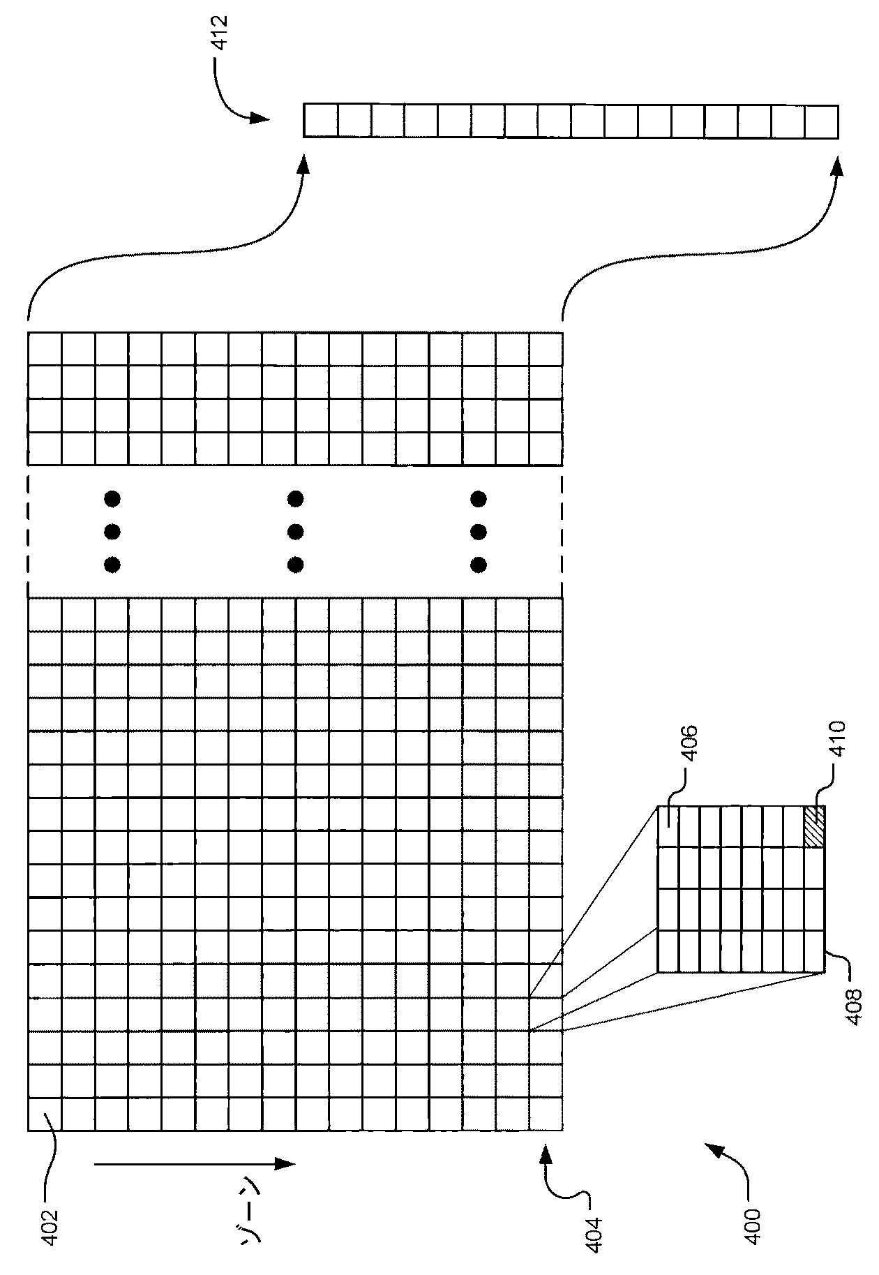
1つの実施例において、メモリーウインドウメッシュは、メッシュエントリーのアレイを含むように定義される。各メッシュエントリーには、複数のアドレス位置が含まれている。メッシュエントリーには、リファレンス位置として指定されるアドレス位置が含まれている。メッシュエントリーのリファレンス位置への書き込みオペレーションが検出される。書き込まれたメッシュエントリーと関係するアクションが、検出オペレーションに応答してトリガーされる。
(1)If(Address&Mask1)==Matchであるならば、メッシュエントリーにおけるリファレンス位置への書き込みが検出される。
(2)Tag=(Address&Mask2)>>5
ここで、AddressはPCI書き込みオペレーションからの書き込みアドレスを表し、Mask1は、バイトオフセットを含まないアドレスビット位置においてクリアであり(例えば、Mask1=0x0000001F)、Mask2は、メッシュインデックスを含むアドレスビット位置においてセットであり(例えば、Mask2=0x001FFFE0)、Matchは、所定のゾーンの所定のメッシュエントリー内のリファレンス位置を表し(例えば、0x0000001F)、シフトは、メッシュインデックスをレジスタの下位ビットに移すのに必要とされるビット数を表す(例えば、表1において与えられる代表的な25ビットアドレスの例においてシフト=5)。この検出ロジックは、リファレンス位置が複数バイト書き込みオペレーションに含まれているとき作用する。したがって、メッシュエントリーにおけるリファレンス位置への書き込みが検出されるならば、書き込みアドレスのメッシュインデックス部分からタグが作り出される。
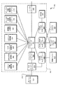
102 ローカルエリアネットワーク
104 ストレージエリアネットワーク
106 アプリケーション顧客
108 アプリケーションサーバー
110 アプリケーションデータストレージデバイス
200 インテリジェントストレージプロセッサー(ISP)基板
202,204 ISPサブシステム
206 広域並列低電圧差動(LVD)バス(eバス)
208,210 インテリジェントストレージプロセッサー
212 ポリシープロセッサー
214 PCIバス
216 ファイバーチャンネルホストリンク
218 ファイバーチャンネルストレージリンク
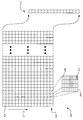
300 ストレージシステム
302 ISP
304 ポリシープロセッサー
306 バッファメモリー
308 キャッシュテーブルメモリー
310 交換メモリー
312 PCIバス
314 ホスト交換制御器
316 ディスク交換制御器(コア1)
318 ディスク交換制御器(コア2)
320 Cmdルーティング制御器
322 DMA/XOR制御器
324 メタデータ制御器
326 雑機能制御器
328 DRAMリストマネージャー
330 DUAL−DRAMリストマネージャー
332 SRAMリストマネージャー
333 SRAM
334 ストレージエンジン
336 Eバスインターフェース
400 リファレンスメッシュ
402 メッシュエントリー
404 ゾーン
412 ゾーンテンプレートレジスタ
Claims (20)
- リファレンス位置として指定されたアドレス位置を含む複数のアドレス位置をそれぞれに有するメッシュエントリのアレイを備えたメモリウインドウメッシュを画定し、
メッシュエントリーのリファレンス位置への書き込みオペレーションを検出し、
検出オペレーションに応答して、書き込まれたメッシュエントリーと関連するアクションをトリガーする、
ステップを含む、書き込みリファレンスメッシュを構成する方法。 - メモリーウインドウメッシュがゾーンに分割されており、各ゾーンには複数のメッシュエントリーが含まれており、かつトリガーされたアクションは、書き込まれたメッシュエントリーが含まれているゾーンと関連している請求項1に記載の方法。
- メモリーウインドウメッシュがゾーンに分割されており、各ゾーンは、トリガーされるべきアクションを指定するアクションディスクリプターと関連している請求項1に記載の方法。
- 検出された書き込みオペレーションが、第一のメモリーのメモリーアドレスに向けられており、かつトリガーを行うオペレーションが、第二のメモリーのメモリーアドレスに向けられる別の書き込みオペレーションをトリガーする請求項1に記載の方法。
- 第二のメモリーに書き込まれるメモリーアドレスが、書き込まれたメッシュエントリーの含まれるゾーンに依存する請求項4に記載の方法。
- 第二のメモリーに書き込まれたメモリーアドレスが、第一のメモリーに書き込まれたメッシュエントリーに依存する請求項4に記載の方法。
- 第二のメモリーに書き込まれたメモリーアドレスが、第一のメモリーに書き込まれたメモリーアドレスのメッシュインデックスに依存する請求項4に記載の方法。
- トリガーするオペレーションが、メッセージを生成し、そのメッセージをメッセージプロセッサーに送る請求項1に記載の方法。
- 生成されるメッセージが、書き込まれたメッシュエントリーの含まれているゾーンに依存する請求項8に記載の方法。
- 生成されるメッセージが、第一のメモリーに書き込まれたメッシュエントリーに依存する請求項8に記載の方法。
- 生成されるメッセージが、第一のメモリーに書き込まれたメモリーアドレスのメッシュインデックスに依存する請求項8に記載の方法。
- 検出オペレーションが、メッシュエントリーへの書き込みオペレーションが完了するとき検出を行う請求項1に記載の方法。
- 各メッシュエントリーには複数のアドレス位置が含まれており、リファレンス位置が、アクションをトリガーするよう指定されるメッシュエントリーにおける所定のアドレス位置を表し、そうしてメッシュエントリーにおける他のアドレス位置への書き込みオペレーションがアクションをトリガーしないようにする請求項1に記載の方法。
- メッシュエントリーのアレイを含むメモリーウインドウメッシュであって、各メッシュエントリーには複数のアドレス位置が含まれており、メッシュエントリーにはリファレンス位置として指定されるアドレス位置が含まれているメモリーウインドウメッシュと、
書き込まれたメッシュエントリーと関連するアクションを、メッシュエントリーのリファレンス位置への書き込みオペレーションの検出に応答してトリガーするストレージエンジンと
を備える書き込みリファレンスメッシュを構成するシステム。 - メモリーウインドウメッシュがゾーンに分割されており、各ゾーンには複数のメッシュエントリーが含まれており、かつトリガーされるアクションが、書き込まれたメッシュエントリーの含まれているゾーンと関連している請求項14に記載のシステム。
- メモリーウインドウメッシュがゾーンに分割されており、各ゾーンは、トリガーされるべきアクションを指定するアクションディスクリプターと関連している請求項14に記載のシステム。
- 検出される書き込みオペレーションが、第一のメモリーのメモリーアドレスに向けられていて、かつトリガーされるアクションが、第二のメモリーのメモリーアドレスに向けられる別の書き込みオペレーションをトリガーする請求項14に記載のシステム。
- トリガーされるアクションが、メッセージを生成して、そのメッセージをメッセージプロセッサーに送る請求項14に記載のシステム。
- メッシュエントリーのリファレンス位置への書き込みオペレーションの検出が、メッシュエントリーへの書き込みオペレーションが完了するとき検出する請求項14に記載のシステム。
- 各メッシュエントリーには複数のアドレス位置が含まれており、リファレンス位置が、アクションをトリガーするよう指定されるメッシュエントリーにおける所定のアドレス位置を表し、そうしてメッシュエントリーにおける他のアドレス位置への書き込みオペレーションがアクションをトリガーしないようにする請求項14に記載のシステム。
Applications Claiming Priority (1)
| Application Number | Priority Date | Filing Date | Title |
|---|---|---|---|
| US11/042,424 US7287128B1 (en) | 2005-01-25 | 2005-01-25 | Write on reference mesh |
Publications (2)
| Publication Number | Publication Date |
|---|---|
| JP2006209727A true JP2006209727A (ja) | 2006-08-10 |
| JP4679963B2 JP4679963B2 (ja) | 2011-05-11 |
Family
ID=36966468
Family Applications (1)
| Application Number | Title | Priority Date | Filing Date |
|---|---|---|---|
| JP2005142907A Expired - Fee Related JP4679963B2 (ja) | 2005-01-25 | 2005-05-16 | 書き込みリファレンスメッシュを構成する方法およびシステム |
Country Status (2)
| Country | Link |
|---|---|
| US (1) | US7287128B1 (ja) |
| JP (1) | JP4679963B2 (ja) |
Families Citing this family (1)
| Publication number | Priority date | Publication date | Assignee | Title |
|---|---|---|---|---|
| US8914540B1 (en) * | 2008-07-01 | 2014-12-16 | Cisco Technology, Inc. | Multi-fabric SAN based data migration |
Citations (3)
| Publication number | Priority date | Publication date | Assignee | Title |
|---|---|---|---|---|
| JPH06247010A (ja) * | 1993-02-25 | 1994-09-06 | Oki Electric Ind Co Ltd | プリンタのコマンド処理装置 |
| JPH0772988A (ja) * | 1993-09-06 | 1995-03-17 | Seiko Epson Corp | 情報機器 |
| JP2004523831A (ja) * | 2001-02-13 | 2004-08-05 | キャンデラ, インコーポレイテッド | シリコンベースのストレージ仮想化サーバ |
Family Cites Families (10)
| Publication number | Priority date | Publication date | Assignee | Title |
|---|---|---|---|---|
| US5377344A (en) | 1991-07-31 | 1994-12-27 | Toyo Corporation | Selective memory transaction monitor system |
| US6442585B1 (en) | 1997-11-26 | 2002-08-27 | Compaq Computer Corporation | Method for scheduling contexts based on statistics of memory system interactions in a computer system |
| US6202127B1 (en) | 1997-11-26 | 2001-03-13 | Compaq Computer Corporation | Apparatus for spatial and temporal sampling in a computer memory system |
| US6601149B1 (en) | 1999-12-14 | 2003-07-29 | International Business Machines Corporation | Memory transaction monitoring system and user interface |
| US6742101B2 (en) | 2001-06-29 | 2004-05-25 | Fujitsu Limited | Scalable and flexible method for address space decoding in a multiple node computer system |
| US6862634B2 (en) | 2001-06-29 | 2005-03-01 | Fujitsu Limited | Mechanism to improve performance in a multi-node computer system |
| US7213081B2 (en) | 2001-06-29 | 2007-05-01 | Fujitsu Limited | Dynamic determination of memory mapped input output range granularity for multi-node computer system |
| US6970809B2 (en) | 2001-08-29 | 2005-11-29 | International Business Machines Corporation | Automated configuration of on-circuit facilities |
| US7120728B2 (en) * | 2002-07-31 | 2006-10-10 | Brocade Communications Systems, Inc. | Hardware-based translating virtualization switch |
| US7334077B2 (en) * | 2003-10-17 | 2008-02-19 | Renesas Technology America, Inc. | Method and apparatus for smart memory pass-through communication |
-
2005
- 2005-01-25 US US11/042,424 patent/US7287128B1/en not_active Expired - Fee Related
- 2005-05-16 JP JP2005142907A patent/JP4679963B2/ja not_active Expired - Fee Related
Patent Citations (3)
| Publication number | Priority date | Publication date | Assignee | Title |
|---|---|---|---|---|
| JPH06247010A (ja) * | 1993-02-25 | 1994-09-06 | Oki Electric Ind Co Ltd | プリンタのコマンド処理装置 |
| JPH0772988A (ja) * | 1993-09-06 | 1995-03-17 | Seiko Epson Corp | 情報機器 |
| JP2004523831A (ja) * | 2001-02-13 | 2004-08-05 | キャンデラ, インコーポレイテッド | シリコンベースのストレージ仮想化サーバ |
Also Published As
| Publication number | Publication date |
|---|---|
| JP4679963B2 (ja) | 2011-05-11 |
| US7287128B1 (en) | 2007-10-23 |
Similar Documents
| Publication | Publication Date | Title |
|---|---|---|
| EP1606712B1 (en) | System and method for dynamic mirror-bank addressing | |
| US11048569B1 (en) | Adaptive timeout mechanism | |
| USRE44610E1 (en) | Node identification for distributed shared memory system | |
| US7562176B2 (en) | Apparatus and methods for clustering multiple independent PCI express hierarchies | |
| US7496698B2 (en) | System and method for efficient implementation of a shared receive queue | |
| US10846163B1 (en) | Hybrid hardware and software reporting management | |
| US10762137B1 (en) | Page table search engine | |
| WO2022007644A1 (zh) | 多处理器系统及配置多处理器系统的方法 | |
| KR101575070B1 (ko) | 디바이스 기능에 대한 액세스를 제공하기 위한 장치, 시스템 및 방법 | |
| US10810133B1 (en) | Address translation and address translation memory for storage class memory | |
| KR102792263B1 (ko) | 메모리 카드 및 이를 이용한 데이터 처리 방법 | |
| CN117827449B (zh) | 服务器的物理内存扩展架构、服务器、方法、设备及介质 | |
| KR102964796B1 (ko) | 컴퓨팅 시스템에서의 메모리 티어링 기법 | |
| JP7856240B2 (ja) | コンピューティング・システムにおけるメモリ動作管理 | |
| US10437750B2 (en) | Relative data width indication for read responses routed by an interconnect | |
| US20060277350A1 (en) | Stripe buffer list | |
| BR112016003488B1 (pt) | Sistema de armazenamento, método, e aparelho para processar solicitação de operação | |
| JP4679963B2 (ja) | 書き込みリファレンスメッシュを構成する方法およびシステム | |
| US10754789B1 (en) | Address translation for storage class memory in a system that includes virtual machines | |
| CN110945843A (zh) | 虚拟交换设备和方法 | |
| US10402329B1 (en) | Reducing traffic in hierarchical cache interconnects | |
| JP4446961B2 (ja) | 要求を送るための集積回路および方法 | |
| KR20230116887A (ko) | 네트워크 통신 링크의 요청 패킷들에 대한 태그들 | |
| US7424496B1 (en) | Asymmetric coherency protection | |
| CN102236572B (zh) | 一种加载固件的方法和设备 |
Legal Events
| Date | Code | Title | Description |
|---|---|---|---|
| A621 | Written request for application examination |
Free format text: JAPANESE INTERMEDIATE CODE: A621 Effective date: 20080512 |
|
| RD03 | Notification of appointment of power of attorney |
Free format text: JAPANESE INTERMEDIATE CODE: A7423 Effective date: 20100526 |
|
| A977 | Report on retrieval |
Free format text: JAPANESE INTERMEDIATE CODE: A971007 Effective date: 20101228 |
|
| TRDD | Decision of grant or rejection written | ||
| A01 | Written decision to grant a patent or to grant a registration (utility model) |
Free format text: JAPANESE INTERMEDIATE CODE: A01 Effective date: 20110118 |
|
| A01 | Written decision to grant a patent or to grant a registration (utility model) |
Free format text: JAPANESE INTERMEDIATE CODE: A01 |
|
| A61 | First payment of annual fees (during grant procedure) |
Free format text: JAPANESE INTERMEDIATE CODE: A61 Effective date: 20110202 |
|
| R150 | Certificate of patent or registration of utility model |
Free format text: JAPANESE INTERMEDIATE CODE: R150 |
|
| FPAY | Renewal fee payment (event date is renewal date of database) |
Free format text: PAYMENT UNTIL: 20140210 Year of fee payment: 3 |
|
| R250 | Receipt of annual fees |
Free format text: JAPANESE INTERMEDIATE CODE: R250 |
|
| R250 | Receipt of annual fees |
Free format text: JAPANESE INTERMEDIATE CODE: R250 |
|
| LAPS | Cancellation because of no payment of annual fees |