JP2006295129A - 耐久性を向上させたエキシマレーザ用素子 - Google Patents
耐久性を向上させたエキシマレーザ用素子 Download PDFInfo
- Publication number
- JP2006295129A JP2006295129A JP2006026853A JP2006026853A JP2006295129A JP 2006295129 A JP2006295129 A JP 2006295129A JP 2006026853 A JP2006026853 A JP 2006026853A JP 2006026853 A JP2006026853 A JP 2006026853A JP 2006295129 A JP2006295129 A JP 2006295129A
- Authority
- JP
- Japan
- Prior art keywords
- layer
- aluminum
- dielectric material
- dielectric
- substrate
- Prior art date
- Legal status (The legal status is an assumption and is not a legal conclusion. Google has not performed a legal analysis and makes no representation as to the accuracy of the status listed.)
- Granted
Links
- 150000002500 ions Chemical class 0.000 claims abstract description 37
- 239000000463 material Substances 0.000 claims abstract description 31
- 238000000576 coating method Methods 0.000 claims abstract description 26
- 239000011248 coating agent Substances 0.000 claims abstract description 25
- 239000010410 layer Substances 0.000 claims description 77
- 229910052782 aluminium Inorganic materials 0.000 claims description 67
- XAGFODPZIPBFFR-UHFFFAOYSA-N aluminium Chemical compound [Al] XAGFODPZIPBFFR-UHFFFAOYSA-N 0.000 claims description 67
- 238000000151 deposition Methods 0.000 claims description 59
- 230000008021 deposition Effects 0.000 claims description 44
- 239000003989 dielectric material Substances 0.000 claims description 42
- 239000000758 substrate Substances 0.000 claims description 34
- 239000001301 oxygen Substances 0.000 claims description 27
- 229910052760 oxygen Inorganic materials 0.000 claims description 27
- 239000011261 inert gas Substances 0.000 claims description 26
- 238000000034 method Methods 0.000 claims description 23
- 229910004298 SiO 2 Inorganic materials 0.000 claims description 14
- 239000011521 glass Substances 0.000 claims description 11
- -1 oxygen ions Chemical class 0.000 claims description 11
- PXHVJJICTQNCMI-UHFFFAOYSA-N Nickel Chemical compound [Ni] PXHVJJICTQNCMI-UHFFFAOYSA-N 0.000 claims description 10
- 230000003287 optical effect Effects 0.000 claims description 9
- 239000012790 adhesive layer Substances 0.000 claims description 8
- 230000001681 protective effect Effects 0.000 claims description 7
- 229910018072 Al 2 O 3 Inorganic materials 0.000 claims description 6
- VYZAMTAEIAYCRO-UHFFFAOYSA-N Chromium Chemical compound [Cr] VYZAMTAEIAYCRO-UHFFFAOYSA-N 0.000 claims description 5
- 229910052751 metal Inorganic materials 0.000 claims description 5
- 239000002184 metal Substances 0.000 claims description 5
- 239000000203 mixture Substances 0.000 claims description 5
- 229910052759 nickel Inorganic materials 0.000 claims description 5
- 239000000853 adhesive Substances 0.000 claims description 4
- 230000001070 adhesive effect Effects 0.000 claims description 4
- 239000011651 chromium Substances 0.000 claims description 4
- 229910052804 chromium Inorganic materials 0.000 claims description 4
- 239000002241 glass-ceramic Substances 0.000 claims description 3
- 229910000623 nickel–chromium alloy Inorganic materials 0.000 claims description 3
- 238000001771 vacuum deposition Methods 0.000 claims description 3
- 238000010030 laminating Methods 0.000 claims 8
- 229910045601 alloy Inorganic materials 0.000 claims 4
- 239000000956 alloy Substances 0.000 claims 4
- 150000002739 metals Chemical class 0.000 claims 3
- 239000000919 ceramic Substances 0.000 claims 1
- 230000008016 vaporization Effects 0.000 claims 1
- VYPSYNLAJGMNEJ-UHFFFAOYSA-N Silicium dioxide Chemical compound O=[Si]=O VYPSYNLAJGMNEJ-UHFFFAOYSA-N 0.000 abstract description 22
- 239000000377 silicon dioxide Substances 0.000 abstract description 9
- 238000001459 lithography Methods 0.000 abstract description 6
- TWNQGVIAIRXVLR-UHFFFAOYSA-N oxo(oxoalumanyloxy)alumane Chemical compound O=[Al]O[Al]=O TWNQGVIAIRXVLR-UHFFFAOYSA-N 0.000 abstract description 3
- 235000012239 silicon dioxide Nutrition 0.000 abstract description 2
- BOXJYHMFXVNZMY-UHFFFAOYSA-N [Si](=O)=O.[F] Chemical compound [Si](=O)=O.[F] BOXJYHMFXVNZMY-UHFFFAOYSA-N 0.000 abstract 1
- 239000010408 film Substances 0.000 description 40
- QVGXLLKOCUKJST-UHFFFAOYSA-N atomic oxygen Chemical compound [O] QVGXLLKOCUKJST-UHFFFAOYSA-N 0.000 description 18
- 230000010076 replication Effects 0.000 description 9
- 238000002310 reflectometry Methods 0.000 description 7
- 238000004140 cleaning Methods 0.000 description 6
- XKRFYHLGVUSROY-UHFFFAOYSA-N Argon Chemical compound [Ar] XKRFYHLGVUSROY-UHFFFAOYSA-N 0.000 description 5
- 229910052786 argon Inorganic materials 0.000 description 5
- 238000004519 manufacturing process Methods 0.000 description 5
- 230000003647 oxidation Effects 0.000 description 5
- 238000007254 oxidation reaction Methods 0.000 description 5
- 230000015572 biosynthetic process Effects 0.000 description 4
- 229910052731 fluorine Inorganic materials 0.000 description 4
- 239000007789 gas Substances 0.000 description 4
- 238000010438 heat treatment Methods 0.000 description 4
- 239000012528 membrane Substances 0.000 description 4
- YCKRFDGAMUMZLT-UHFFFAOYSA-N Fluorine atom Chemical compound [F] YCKRFDGAMUMZLT-UHFFFAOYSA-N 0.000 description 3
- 229910010293 ceramic material Inorganic materials 0.000 description 3
- 239000011737 fluorine Substances 0.000 description 3
- LIVNPJMFVYWSIS-UHFFFAOYSA-N silicon monoxide Chemical compound [Si-]#[O+] LIVNPJMFVYWSIS-UHFFFAOYSA-N 0.000 description 3
- XLYOFNOQVPJJNP-UHFFFAOYSA-N water Chemical compound O XLYOFNOQVPJJNP-UHFFFAOYSA-N 0.000 description 3
- IJGRMHOSHXDMSA-UHFFFAOYSA-N Atomic nitrogen Chemical compound N#N IJGRMHOSHXDMSA-UHFFFAOYSA-N 0.000 description 2
- XUIMIQQOPSSXEZ-UHFFFAOYSA-N Silicon Chemical compound [Si] XUIMIQQOPSSXEZ-UHFFFAOYSA-N 0.000 description 2
- 230000004888 barrier function Effects 0.000 description 2
- 238000011109 contamination Methods 0.000 description 2
- 238000005137 deposition process Methods 0.000 description 2
- 238000013461 design Methods 0.000 description 2
- 238000005516 engineering process Methods 0.000 description 2
- 239000006112 glass ceramic composition Substances 0.000 description 2
- 238000001393 microlithography Methods 0.000 description 2
- 229910052710 silicon Inorganic materials 0.000 description 2
- 239000010703 silicon Substances 0.000 description 2
- 229910052814 silicon oxide Inorganic materials 0.000 description 2
- 239000010409 thin film Substances 0.000 description 2
- 239000004593 Epoxy Substances 0.000 description 1
- CBENFWSGALASAD-UHFFFAOYSA-N Ozone Chemical compound [O-][O+]=O CBENFWSGALASAD-UHFFFAOYSA-N 0.000 description 1
- VRAIHTAYLFXSJJ-UHFFFAOYSA-N alumane Chemical compound [AlH3].[AlH3] VRAIHTAYLFXSJJ-UHFFFAOYSA-N 0.000 description 1
- PNEYBMLMFCGWSK-UHFFFAOYSA-N aluminium oxide Inorganic materials [O-2].[O-2].[O-2].[Al+3].[Al+3] PNEYBMLMFCGWSK-UHFFFAOYSA-N 0.000 description 1
- 238000013459 approach Methods 0.000 description 1
- 239000012298 atmosphere Substances 0.000 description 1
- WUKWITHWXAAZEY-UHFFFAOYSA-L calcium difluoride Chemical compound [F-].[F-].[Ca+2] WUKWITHWXAAZEY-UHFFFAOYSA-L 0.000 description 1
- 229910001634 calcium fluoride Inorganic materials 0.000 description 1
- 230000015556 catabolic process Effects 0.000 description 1
- 238000006243 chemical reaction Methods 0.000 description 1
- 239000003795 chemical substances by application Substances 0.000 description 1
- 239000000356 contaminant Substances 0.000 description 1
- 229910052593 corundum Inorganic materials 0.000 description 1
- 238000006731 degradation reaction Methods 0.000 description 1
- 230000032798 delamination Effects 0.000 description 1
- 238000000280 densification Methods 0.000 description 1
- 230000006866 deterioration Effects 0.000 description 1
- 239000002019 doping agent Substances 0.000 description 1
- 230000000694 effects Effects 0.000 description 1
- 230000005684 electric field Effects 0.000 description 1
- 238000001704 evaporation Methods 0.000 description 1
- 238000010348 incorporation Methods 0.000 description 1
- 238000012423 maintenance Methods 0.000 description 1
- 230000008018 melting Effects 0.000 description 1
- 238000002844 melting Methods 0.000 description 1
- 229910052757 nitrogen Inorganic materials 0.000 description 1
- 238000010943 off-gassing Methods 0.000 description 1
- 238000000206 photolithography Methods 0.000 description 1
- 239000011148 porous material Substances 0.000 description 1
- 239000002243 precursor Substances 0.000 description 1
- 238000012545 processing Methods 0.000 description 1
- 239000011253 protective coating Substances 0.000 description 1
- 238000010926 purge Methods 0.000 description 1
- 229910052705 radium Inorganic materials 0.000 description 1
- HCWPIIXVSYCSAN-UHFFFAOYSA-N radium atom Chemical compound [Ra] HCWPIIXVSYCSAN-UHFFFAOYSA-N 0.000 description 1
- 230000003362 replicative effect Effects 0.000 description 1
- 238000011160 research Methods 0.000 description 1
- 230000035939 shock Effects 0.000 description 1
- 239000002356 single layer Substances 0.000 description 1
- 238000001228 spectrum Methods 0.000 description 1
- 239000007858 starting material Substances 0.000 description 1
- 238000000427 thin-film deposition Methods 0.000 description 1
- 238000007740 vapor deposition Methods 0.000 description 1
- 229910001845 yogo sapphire Inorganic materials 0.000 description 1
Images

Classifications
-
- G02B1/105—
-
- G—PHYSICS
- G02—OPTICS
- G02B—OPTICAL ELEMENTS, SYSTEMS OR APPARATUS
- G02B1/00—Optical elements characterised by the material of which they are made; Optical coatings for optical elements
- G02B1/10—Optical coatings produced by application to, or surface treatment of, optical elements
- G02B1/14—Protective coatings, e.g. hard coatings
-
- G—PHYSICS
- G02—OPTICS
- G02B—OPTICAL ELEMENTS, SYSTEMS OR APPARATUS
- G02B5/00—Optical elements other than lenses
- G02B5/08—Mirrors
- G02B5/0891—Ultraviolet [UV] mirrors
-
- G—PHYSICS
- G02—OPTICS
- G02B—OPTICAL ELEMENTS, SYSTEMS OR APPARATUS
- G02B5/00—Optical elements other than lenses
- G02B5/18—Diffraction gratings
- G02B5/1838—Diffraction gratings for use with ultraviolet radiation or X-rays
-
- G—PHYSICS
- G03—PHOTOGRAPHY; CINEMATOGRAPHY; ANALOGOUS TECHNIQUES USING WAVES OTHER THAN OPTICAL WAVES; ELECTROGRAPHY; HOLOGRAPHY
- G03F—PHOTOMECHANICAL PRODUCTION OF TEXTURED OR PATTERNED SURFACES, e.g. FOR PRINTING, FOR PROCESSING OF SEMICONDUCTOR DEVICES; MATERIALS THEREFOR; ORIGINALS THEREFOR; APPARATUS SPECIALLY ADAPTED THEREFOR
- G03F7/00—Photomechanical, e.g. photolithographic, production of textured or patterned surfaces, e.g. printing surfaces; Materials therefor, e.g. comprising photoresists; Apparatus specially adapted therefor
- G03F7/70—Microphotolithographic exposure; Apparatus therefor
- G03F7/708—Construction of apparatus, e.g. environment aspects, hygiene aspects or materials
- G03F7/7095—Materials, e.g. materials for housing, stage or other support having particular properties, e.g. weight, strength, conductivity, thermal expansion coefficient
- G03F7/70958—Optical materials or coatings, e.g. with particular transmittance, reflectance or anti-reflection properties
-
- G—PHYSICS
- G02—OPTICS
- G02B—OPTICAL ELEMENTS, SYSTEMS OR APPARATUS
- G02B5/00—Optical elements other than lenses
- G02B5/18—Diffraction gratings
- G02B5/1861—Reflection gratings characterised by their structure, e.g. step profile, contours of substrate or grooves, pitch variations, materials
-
- H—ELECTRICITY
- H01—ELECTRIC ELEMENTS
- H01S—DEVICES USING THE PROCESS OF LIGHT AMPLIFICATION BY STIMULATED EMISSION OF RADIATION [LASER] TO AMPLIFY OR GENERATE LIGHT; DEVICES USING STIMULATED EMISSION OF ELECTROMAGNETIC RADIATION IN WAVE RANGES OTHER THAN OPTICAL
- H01S3/00—Lasers, i.e. devices using stimulated emission of electromagnetic radiation in the infrared, visible or ultraviolet wave range
- H01S3/05—Construction or shape of optical resonators; Accommodation of active medium therein; Shape of active medium
- H01S3/08—Construction or shape of optical resonators or components thereof
- H01S3/08059—Constructional details of the reflector, e.g. shape
Landscapes
- Physics & Mathematics (AREA)
- General Physics & Mathematics (AREA)
- Optics & Photonics (AREA)
- Health & Medical Sciences (AREA)
- Environmental & Geological Engineering (AREA)
- Engineering & Computer Science (AREA)
- Toxicology (AREA)
- Epidemiology (AREA)
- Public Health (AREA)
- Diffracting Gratings Or Hologram Optical Elements (AREA)
- Lasers (AREA)
- Optical Elements Other Than Lenses (AREA)
- Surface Treatment Of Optical Elements (AREA)
- Physical Vapour Deposition (AREA)
Abstract
【解決手段】 高エネルギーのイオンプラズマによる衝撃を与えながら被着させることによってコーティングの耐久性の向上を図った。
【選択図】図1
Description
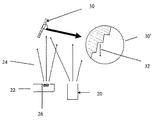
22 るつぼ
24 蒸着物質
26 誘電材料
30” 基板ブレーズ面
50 接着層
60 アルミニウム層
70 誘電体バリア層
Claims (12)
- 基板と、
前記基板の表面に被着されたアルミニウム膜と、
前記アルミニウム膜の前記表面に積層させた、1つまたは複数の保護用誘電材料層と
を備える、高出力エキシマレーザ用の長寿命の素子であって、
1つの誘電材料層を積層させるかまたは複数の誘電材料層の最初の層を被着させるとき、前記1つの誘電材料層または前記最初の誘電材料層を第1の部分および第2の部分として積層させ、前記第1の部分を前記アルミニウム膜の表面に積層させ、前記第2の部分を前記第1の部分の表面に積層させ、
前記第1の部分の被着中、高エネルギーの不活性ガスイオンによる衝撃を前記第1の部分に受けさせ、前記第2の部分の被着中、高エネルギーの不活性ガスイオンと高エネルギーの酸素イオンの組合せによる衝撃を前記第2の部分に受けさせた
ことを特徴とする素子。 - 前記被着させた誘電材料層の厚さが20〜150nmの範囲内にあり、前記厚さは複数層の場合は各層の厚さであることを特徴とする請求項1に記載の素子。
- 前記被着させた1つの誘電材料層または前記被着させた複数の誘電材料層の前記最初の誘電材料層の、前記第1の部分の厚さが4〜8nmの範囲内であり、前記第2の部分の厚さが12〜146nmの範囲内であり、前記第1および第2の部分の総厚が20〜150nmの範囲内であることを特徴とする請求項2に記載の素子。
- 前記誘電材料が、SiO2、Al2O3およびF−SiO2から成る群より選択されることを特徴とする請求項1に記載の素子。
- 前記素子が、反射性かまたは特定の波長帯の光を反射する格子またはミラーから成る群より選択されることを特徴とする請求項1に記載の素子。
- 前記基板がガラスであり、前記素子が接着材料を前記ガラスと前記アルミニウム膜との間にさらに備え、前記接着材料が、ニッケル、クロム、ニッケルクロム合金、ならびにガラスとアルミニウムとを接着するための技術的公知の他の金属および合金から成る群より選択されることを特徴とする請求項1に記載の素子。
- リソグラフィレーザシステム用の素子であって、前記素子が、反射性かまたは特定の波長帯の光を反射する格子またはミラーであり、前記素子が、
ガラス、ガラスセラミックまたはセラミックの基板と、
前記基板の表面に被着されたアルミニウム膜と、
前記基板と前記アルミニウム膜との間の接着層であって、ニッケル、クロム、ニッケルクロム合金、ならびに前記基板とアルミニウムとを接着するための技術的公知の他の金属および合金から成る群より選択される材料を含む接着層と、
前記アルミニウム膜の前記表面に積層させた、1つまたは複数の保護用誘電材料層と
を備え、
1つの誘電材料層を積層させるかまたは複数の誘電材料層の最初の層を被着させるとき、前記1つの誘電材料層または前記最初の誘電材料層を第1の部分および第2の部分として積層させ、前記第1の部分を前記アルミニウム膜の表面に積層させ、前記第2の部分を前記第1の部分の表面に積層させ、
前記第1の部分の被着中、高エネルギーの不活性ガスイオンによる衝撃を前記第1の部分に受けさせ、前記第2の部分の被着中、高エネルギーの不活性ガスイオンと高エネルギーの酸素イオンの組合せによる衝撃を前記第2の部分に受けさせ、
前記1つの誘電材料層または前記複数の誘電材料層の最初の層が、SiO2、Al2O3およびF−SiO2から成る群より選択される
ことを特徴とする素子。 - 各誘電材料層の厚さが20〜150nmの範囲内であることを特徴とする請求項7に記載の素子。
- 前記被着させた1つの誘電材料層または前記被着させた複数の誘電材料層の前記最初の誘電材料層の、前記第1の部分の厚さが4〜8nmの範囲内であり、前記第2の部分の厚さが12〜146nmの範囲内であり、前記第1および第2の部分の総厚が20〜150nmの範囲内であることを特徴とする請求項8に記載の素子。
- 表面にアルミニウムコーティングを備えた光学素子のアルミニウム表面上に稠密な誘電体膜を被着させる方法であって、
基板上にアルミニウム層を有する光学素子を、選択された誘電性コーティング材料のソースと、高エネルギー不活性ガスイオンおよび高エネルギー酸素イオンのソースとを備えた真空蒸着チャンバに入れる工程と、
前記チャンバを圧力9×10⁻⁶mbar未満まで排気する工程と、
コーティング中の前記真空蒸着チャンバ内の圧力が7×10⁻⁵mbar〜4×10⁻⁴の範囲内となるような態様で前記誘電性コーティング材料および高エネルギーのイオンで衝撃しながら前記誘電性コーティング材料を気化して前記アルミニウム表面上に被着させる工程と、
前記誘電性コーティング材料を厚さ20〜150nmの範囲内に被着させ、それによって基板上のアルミニウム層を覆う誘電性コーティングを備えた光学素子を形成する工程と
を有してなる方法であり、
前記誘電性コーティング材料を衝撃する前記工程が、前記誘電性コーティング材料の最初の4〜8nmの被着中にのみ高エネルギーの不活性ガスイオンで衝撃する工程と、前記誘電性コーティング材料の残りの被着中は不活性ガスイオンと酸素イオンの混合物で衝撃する工程とを含む
ことを特徴とする方法。 - 前記アルミニウム膜の前記表面に前記誘電性コーティング材料を被着させる前記工程が、SiO2、Al2O3およびF−SiO2から成る群より選択される材料を被着させる工程を含むことを特徴とする請求項10に記載の方法。
- 光学素子を提供するとは、基板上にアルミニウム層を有し、前記アルミ層と前記基板との間に接着層を有する光学素子を提供することであり、前記接着層が、ニッケル、クロム、ニッケルクロム合金、ならびに前記基板とアルミニウムとを接着するための技術的公知の他の金属および合金から成る群より選択されることを特徴とする請求項10に記載の方法。
Applications Claiming Priority (2)
| Application Number | Priority Date | Filing Date | Title |
|---|---|---|---|
| US11/050,986 | 2005-02-03 | ||
| US11/050,986 US7561611B2 (en) | 2005-02-03 | 2005-02-03 | Extended-lifetime elements for excimer lasers |
Related Child Applications (1)
| Application Number | Title | Priority Date | Filing Date |
|---|---|---|---|
| JP2014090391A Division JP2014194550A (ja) | 2005-02-03 | 2014-04-24 | 耐久性を向上させたエキシマレーザ用素子 |
Publications (2)
| Publication Number | Publication Date |
|---|---|
| JP2006295129A true JP2006295129A (ja) | 2006-10-26 |
| JP5642914B2 JP5642914B2 (ja) | 2014-12-17 |
Family
ID=36709923
Family Applications (3)
| Application Number | Title | Priority Date | Filing Date |
|---|---|---|---|
| JP2006026853A Expired - Fee Related JP5642914B2 (ja) | 2005-02-03 | 2006-02-03 | 耐久性を向上させたエキシマレーザ用素子 |
| JP2014090391A Pending JP2014194550A (ja) | 2005-02-03 | 2014-04-24 | 耐久性を向上させたエキシマレーザ用素子 |
| JP2016198824A Pending JP2017027077A (ja) | 2005-02-03 | 2016-10-07 | 耐久性を向上させたエキシマレーザ用素子 |
Family Applications After (2)
| Application Number | Title | Priority Date | Filing Date |
|---|---|---|---|
| JP2014090391A Pending JP2014194550A (ja) | 2005-02-03 | 2014-04-24 | 耐久性を向上させたエキシマレーザ用素子 |
| JP2016198824A Pending JP2017027077A (ja) | 2005-02-03 | 2016-10-07 | 耐久性を向上させたエキシマレーザ用素子 |
Country Status (3)
| Country | Link |
|---|---|
| US (1) | US7561611B2 (ja) |
| JP (3) | JP5642914B2 (ja) |
| DE (1) | DE102006004835B4 (ja) |
Cited By (2)
| Publication number | Priority date | Publication date | Assignee | Title |
|---|---|---|---|---|
| KR20150028255A (ko) * | 2012-05-31 | 2015-03-13 | 코닝 인코포레이티드 | 실리카-개질된-플루오르화물 넓은 각도 반사-방지 코팅 |
| JP2022028415A (ja) * | 2020-08-03 | 2022-02-16 | 株式会社島津製作所 | ブレーズド回折格子およびブレーズド回折格子の製造方法 |
Families Citing this family (3)
| Publication number | Priority date | Publication date | Assignee | Title |
|---|---|---|---|---|
| DE102018221189A1 (de) | 2018-12-07 | 2020-06-10 | Carl Zeiss Smt Gmbh | Verfahren zum Bilden von Nanostrukturen an einer Oberfläche und optisches Element |
| DE102019200208A1 (de) | 2019-01-10 | 2020-07-16 | Carl Zeiss Smt Gmbh | Verfahren zum in situ dynamischen Schutz einer Oberfläche und optische Anordnung |
| DE102021200747A1 (de) | 2021-01-28 | 2022-07-28 | Carl Zeiss Smt Gmbh | Verfahren zum Bilden einer Schicht, optisches Element und optisches System |
Citations (16)
| Publication number | Priority date | Publication date | Assignee | Title |
|---|---|---|---|---|
| JPS57157204A (en) * | 1981-02-27 | 1982-09-28 | Siemens Ag | Laser reflector and manufacture thereof |
| JPH02287302A (ja) * | 1989-04-27 | 1990-11-27 | Copal Co Ltd | シリカゲル保護膜付射鏡及びその製法 |
| JPH06102407A (ja) * | 1992-09-18 | 1994-04-15 | Hitachi Ltd | レプリカ回折格子 |
| JPH07239407A (ja) * | 1994-02-28 | 1995-09-12 | Shimadzu Corp | レプリカ回折格子 |
| JPH0815514A (ja) * | 1994-06-24 | 1996-01-19 | Canon Inc | 反射型回折格子 |
| JPH08304614A (ja) * | 1995-05-12 | 1996-11-22 | Ricoh Co Ltd | 合成樹脂製反射鏡、その製造方法および製造装置 |
| JPH09104969A (ja) * | 1995-08-09 | 1997-04-22 | Matsushita Electric Ind Co Ltd | 導体膜およびその形成方法 |
| JPH11160513A (ja) * | 1997-09-29 | 1999-06-18 | Cymer Inc | レプリカ回折格子の保護被膜 |
| JP2000077762A (ja) * | 1998-05-20 | 2000-03-14 | Cymer Inc | 高信頼性・モジュラ製造高品質狭帯域高繰り返しレ―トArFエキシマレ―ザ |
| JP2000081505A (ja) * | 1998-09-04 | 2000-03-21 | Nikon Corp | 反射鏡及び反射鏡の製造方法 |
| JP2002339084A (ja) * | 2001-03-13 | 2002-11-27 | Kiyousera Opt Kk | 金属膜および金属膜被覆部材 |
| JP2003105534A (ja) * | 2001-09-27 | 2003-04-09 | Ulvac Japan Ltd | 光学薄膜の成膜方法及び成膜装置 |
| JP2004035941A (ja) * | 2002-07-03 | 2004-02-05 | Konica Minolta Holdings Inc | 表面処理方法及び光学部品 |
| JP2004514794A (ja) * | 2000-12-07 | 2004-05-20 | サイマー, インコーポレイテッド | 複製された回折格子のための保護膜 |
| JP2004170757A (ja) * | 2002-11-21 | 2004-06-17 | Victor Co Of Japan Ltd | 液晶プロジェクタ装置用偏光板及びその製造方法 |
| US20050008879A1 (en) * | 2003-06-27 | 2005-01-13 | Asahi Glass Company Limited | High reflectance mirror |
Family Cites Families (19)
| Publication number | Priority date | Publication date | Assignee | Title |
|---|---|---|---|---|
| US4223974A (en) | 1978-08-02 | 1980-09-23 | American Optical Corporation | Enhanced bonding of silicon oxides and silver by intermediate coating of metal |
| JPS5689702A (en) * | 1979-12-21 | 1981-07-21 | Sumitomo Electric Ind Ltd | Laser beam reflecting mirror |
| JPH0820574B2 (ja) * | 1987-03-06 | 1996-03-04 | 住友電気工業株式会社 | 分散シフトフアイバ及びその製造方法 |
| JPS6318624A (ja) * | 1986-07-11 | 1988-01-26 | Matsushita Electric Ind Co Ltd | 露光装置 |
| US5027101A (en) * | 1987-01-22 | 1991-06-25 | Morrill Jr Vaughan | Sub-miniature fuse |
| EP0332790B1 (en) | 1988-03-18 | 1994-11-30 | Instruments S.A. | Improved diffraction grating and method of making |
| JPH0644549B2 (ja) * | 1989-03-17 | 1994-06-08 | 株式会社日立製作所 | 投影露光法及び装置 |
| US5493393A (en) | 1989-03-17 | 1996-02-20 | The Boeing Company | Planar waveguide spectrograph |
| JP3147481B2 (ja) | 1992-04-21 | 2001-03-19 | 松下電器産業株式会社 | ガラス製回折格子の成形用金型及びその製造方法及びガラス製回折格子の製造方法 |
| GB2273623B (en) * | 1992-12-15 | 1996-12-04 | Northern Telecom Ltd | Optical transmission system |
| US5846649A (en) | 1994-03-03 | 1998-12-08 | Monsanto Company | Highly durable and abrasion-resistant dielectric coatings for lenses |
| DE69827604T2 (de) | 1997-01-17 | 2005-04-28 | Cymer, Inc., San Diego | Reflektierender überzug für wiederholtes beugungsgitter |
| JP3624082B2 (ja) * | 1997-11-13 | 2005-02-23 | キヤノン株式会社 | 反射防止膜及びその製造方法 |
| JPH11311704A (ja) * | 1998-02-26 | 1999-11-09 | Nikon Corp | 紫外光用ミラー |
| US6466365B1 (en) * | 2000-04-07 | 2002-10-15 | Corning Incorporated | Film coated optical lithography elements and method of making |
| JP2002040207A (ja) * | 2000-07-27 | 2002-02-06 | Canon Inc | 光学付加膜及び光学素子 |
| JP2002189112A (ja) * | 2000-12-22 | 2002-07-05 | Canon Inc | 回折光学素子の製造方法、回折光学素子の製造方法によって製造したことを特徴とする回折光学素子製造用金型、回折光学素子、および該回折光学素子を有する光学系、光学機器、露光装置、デバイス製造方法、デバイス |
| JP2005017543A (ja) * | 2003-06-25 | 2005-01-20 | Nikon Corp | 紫外線レーザ光用ミラー及び光学系及び投影露光装置 |
| WO2006053705A1 (de) | 2004-11-17 | 2006-05-26 | Carl Zeiss Smt Ag | Verfahren zum schutz eines metallspiegels gegen degradation sowie metallspiegel |
-
2005
- 2005-02-03 US US11/050,986 patent/US7561611B2/en not_active Expired - Fee Related
-
2006
- 2006-02-02 DE DE102006004835.0A patent/DE102006004835B4/de not_active Expired - Fee Related
- 2006-02-03 JP JP2006026853A patent/JP5642914B2/ja not_active Expired - Fee Related
-
2014
- 2014-04-24 JP JP2014090391A patent/JP2014194550A/ja active Pending
-
2016
- 2016-10-07 JP JP2016198824A patent/JP2017027077A/ja active Pending
Patent Citations (16)
| Publication number | Priority date | Publication date | Assignee | Title |
|---|---|---|---|---|
| JPS57157204A (en) * | 1981-02-27 | 1982-09-28 | Siemens Ag | Laser reflector and manufacture thereof |
| JPH02287302A (ja) * | 1989-04-27 | 1990-11-27 | Copal Co Ltd | シリカゲル保護膜付射鏡及びその製法 |
| JPH06102407A (ja) * | 1992-09-18 | 1994-04-15 | Hitachi Ltd | レプリカ回折格子 |
| JPH07239407A (ja) * | 1994-02-28 | 1995-09-12 | Shimadzu Corp | レプリカ回折格子 |
| JPH0815514A (ja) * | 1994-06-24 | 1996-01-19 | Canon Inc | 反射型回折格子 |
| JPH08304614A (ja) * | 1995-05-12 | 1996-11-22 | Ricoh Co Ltd | 合成樹脂製反射鏡、その製造方法および製造装置 |
| JPH09104969A (ja) * | 1995-08-09 | 1997-04-22 | Matsushita Electric Ind Co Ltd | 導体膜およびその形成方法 |
| JPH11160513A (ja) * | 1997-09-29 | 1999-06-18 | Cymer Inc | レプリカ回折格子の保護被膜 |
| JP2000077762A (ja) * | 1998-05-20 | 2000-03-14 | Cymer Inc | 高信頼性・モジュラ製造高品質狭帯域高繰り返しレ―トArFエキシマレ―ザ |
| JP2000081505A (ja) * | 1998-09-04 | 2000-03-21 | Nikon Corp | 反射鏡及び反射鏡の製造方法 |
| JP2004514794A (ja) * | 2000-12-07 | 2004-05-20 | サイマー, インコーポレイテッド | 複製された回折格子のための保護膜 |
| JP2002339084A (ja) * | 2001-03-13 | 2002-11-27 | Kiyousera Opt Kk | 金属膜および金属膜被覆部材 |
| JP2003105534A (ja) * | 2001-09-27 | 2003-04-09 | Ulvac Japan Ltd | 光学薄膜の成膜方法及び成膜装置 |
| JP2004035941A (ja) * | 2002-07-03 | 2004-02-05 | Konica Minolta Holdings Inc | 表面処理方法及び光学部品 |
| JP2004170757A (ja) * | 2002-11-21 | 2004-06-17 | Victor Co Of Japan Ltd | 液晶プロジェクタ装置用偏光板及びその製造方法 |
| US20050008879A1 (en) * | 2003-06-27 | 2005-01-13 | Asahi Glass Company Limited | High reflectance mirror |
Cited By (5)
| Publication number | Priority date | Publication date | Assignee | Title |
|---|---|---|---|---|
| KR20150028255A (ko) * | 2012-05-31 | 2015-03-13 | 코닝 인코포레이티드 | 실리카-개질된-플루오르화물 넓은 각도 반사-방지 코팅 |
| JP2015526749A (ja) * | 2012-05-31 | 2015-09-10 | コーニング インコーポレイテッド | シリカ修飾フッ化物の広角度反射防止コーティング |
| KR102125986B1 (ko) * | 2012-05-31 | 2020-06-24 | 코닝 인코포레이티드 | 실리카-개질된-플루오르화물 넓은 각도 반사-방지 코팅 |
| JP2022028415A (ja) * | 2020-08-03 | 2022-02-16 | 株式会社島津製作所 | ブレーズド回折格子およびブレーズド回折格子の製造方法 |
| JP7581692B2 (ja) | 2020-08-03 | 2024-11-13 | 株式会社島津製作所 | ブレーズド回折格子およびブレーズド回折格子の製造方法 |
Also Published As
| Publication number | Publication date |
|---|---|
| JP2014194550A (ja) | 2014-10-09 |
| US20060171438A1 (en) | 2006-08-03 |
| DE102006004835A1 (de) | 2006-08-10 |
| JP2017027077A (ja) | 2017-02-02 |
| DE102006004835B4 (de) | 2019-01-03 |
| JP5642914B2 (ja) | 2014-12-17 |
| US7561611B2 (en) | 2009-07-14 |
Similar Documents
| Publication | Publication Date | Title |
|---|---|---|
| JP7581459B2 (ja) | Euvリソグラフィ用のメンブレン | |
| JP4549019B2 (ja) | 複製された回折格子のための保護膜 | |
| JP2017027077A (ja) | 耐久性を向上させたエキシマレーザ用素子 | |
| EP1027172B1 (en) | Protective overcoat for replicated diffraction gratings | |
| KR20220130786A (ko) | 극자외선 마스크 블랭크 하드 마스크 재료들 | |
| KR101991530B1 (ko) | 안정된 조성을 갖는 옥시나이트라이드 캐핑층을 포함하는 euv 미러, euv 리소그래피 장치, 및 그 작동 방법 | |
| KR102823804B1 (ko) | 반사형 마스크 블랭크 및 반사형 마스크의 제조 방법 | |
| TWI835896B (zh) | 具有後側塗層的極紫外線掩模 | |
| JPH0336402B2 (ja) |
Legal Events
| Date | Code | Title | Description |
|---|---|---|---|
| A621 | Written request for application examination |
Free format text: JAPANESE INTERMEDIATE CODE: A621 Effective date: 20081003 |
|
| A977 | Report on retrieval |
Free format text: JAPANESE INTERMEDIATE CODE: A971007 Effective date: 20110729 |
|
| A131 | Notification of reasons for refusal |
Free format text: JAPANESE INTERMEDIATE CODE: A131 Effective date: 20110816 |
|
| A601 | Written request for extension of time |
Free format text: JAPANESE INTERMEDIATE CODE: A601 Effective date: 20111116 |
|
| A602 | Written permission of extension of time |
Free format text: JAPANESE INTERMEDIATE CODE: A602 Effective date: 20111121 |
|
| A601 | Written request for extension of time |
Free format text: JAPANESE INTERMEDIATE CODE: A601 Effective date: 20111216 |
|
| A602 | Written permission of extension of time |
Free format text: JAPANESE INTERMEDIATE CODE: A602 Effective date: 20111226 |
|
| A521 | Request for written amendment filed |
Free format text: JAPANESE INTERMEDIATE CODE: A523 Effective date: 20120216 |
|
| A131 | Notification of reasons for refusal |
Free format text: JAPANESE INTERMEDIATE CODE: A131 Effective date: 20121113 |
|
| A601 | Written request for extension of time |
Free format text: JAPANESE INTERMEDIATE CODE: A601 Effective date: 20130213 |
|
| A602 | Written permission of extension of time |
Free format text: JAPANESE INTERMEDIATE CODE: A602 Effective date: 20130218 |
|
| A601 | Written request for extension of time |
Free format text: JAPANESE INTERMEDIATE CODE: A601 Effective date: 20130313 |
|
| A602 | Written permission of extension of time |
Free format text: JAPANESE INTERMEDIATE CODE: A602 Effective date: 20130327 |
|
| A601 | Written request for extension of time |
Free format text: JAPANESE INTERMEDIATE CODE: A601 Effective date: 20130415 |
|
| A602 | Written permission of extension of time |
Free format text: JAPANESE INTERMEDIATE CODE: A602 Effective date: 20130418 |
|
| A521 | Request for written amendment filed |
Free format text: JAPANESE INTERMEDIATE CODE: A523 Effective date: 20130513 |
|
| A02 | Decision of refusal |
Free format text: JAPANESE INTERMEDIATE CODE: A02 Effective date: 20131224 |
|
| A521 | Request for written amendment filed |
Free format text: JAPANESE INTERMEDIATE CODE: A523 Effective date: 20140424 |
|
| A911 | Transfer to examiner for re-examination before appeal (zenchi) |
Free format text: JAPANESE INTERMEDIATE CODE: A911 Effective date: 20140507 |
|
| A131 | Notification of reasons for refusal |
Free format text: JAPANESE INTERMEDIATE CODE: A131 Effective date: 20140708 |
|
| A521 | Request for written amendment filed |
Free format text: JAPANESE INTERMEDIATE CODE: A523 Effective date: 20140728 |
|
| TRDD | Decision of grant or rejection written | ||
| A01 | Written decision to grant a patent or to grant a registration (utility model) |
Free format text: JAPANESE INTERMEDIATE CODE: A01 Effective date: 20140930 |
|
| A61 | First payment of annual fees (during grant procedure) |
Free format text: JAPANESE INTERMEDIATE CODE: A61 Effective date: 20141030 |
|
| R150 | Certificate of patent or registration of utility model |
Ref document number: 5642914 Country of ref document: JP Free format text: JAPANESE INTERMEDIATE CODE: R150 |
|
| R250 | Receipt of annual fees |
Free format text: JAPANESE INTERMEDIATE CODE: R250 |
|
| R250 | Receipt of annual fees |
Free format text: JAPANESE INTERMEDIATE CODE: R250 |
|
| LAPS | Cancellation because of no payment of annual fees |