JP2006303003A - Printed circuit board and information processing apparatus - Google Patents
Printed circuit board and information processing apparatus Download PDFInfo
- Publication number
- JP2006303003A JP2006303003A JP2005119579A JP2005119579A JP2006303003A JP 2006303003 A JP2006303003 A JP 2006303003A JP 2005119579 A JP2005119579 A JP 2005119579A JP 2005119579 A JP2005119579 A JP 2005119579A JP 2006303003 A JP2006303003 A JP 2006303003A
- Authority
- JP
- Japan
- Prior art keywords
- region
- pad
- semiconductor chip
- printed circuit
- circuit board
- Prior art date
- Legal status (The legal status is an assumption and is not a legal conclusion. Google has not performed a legal analysis and makes no representation as to the accuracy of the status listed.)
- Pending
Links
Images


Classifications
-
- G—PHYSICS
- G06—COMPUTING OR CALCULATING; COUNTING
- G06F—ELECTRIC DIGITAL DATA PROCESSING
- G06F1/00—Details not covered by groups G06F3/00 - G06F13/00 and G06F21/00
- G06F1/16—Constructional details or arrangements
- G06F1/1613—Constructional details or arrangements for portable computers
- G06F1/1615—Constructional details or arrangements for portable computers with several enclosures having relative motions, each enclosure supporting at least one I/O or computing function
- G06F1/1616—Constructional details or arrangements for portable computers with several enclosures having relative motions, each enclosure supporting at least one I/O or computing function with folding flat displays, e.g. laptop computers or notebooks having a clamshell configuration, with body parts pivoting to an open position around an axis parallel to the plane they define in closed position
-
- G—PHYSICS
- G06—COMPUTING OR CALCULATING; COUNTING
- G06F—ELECTRIC DIGITAL DATA PROCESSING
- G06F1/00—Details not covered by groups G06F3/00 - G06F13/00 and G06F21/00
- G06F1/16—Constructional details or arrangements
- G06F1/1613—Constructional details or arrangements for portable computers
- G06F1/1633—Constructional details or arrangements of portable computers not specific to the type of enclosures covered by groups G06F1/1615 - G06F1/1626
- G06F1/1656—Details related to functional adaptations of the enclosure, e.g. to provide protection against EMI, shock, water, or to host detachable peripherals like a mouse or removable expansions units like PCMCIA cards, or to provide access to internal components for maintenance or to removable storage supports like CDs or DVDs, or to mechanically mount accessories
-
- G—PHYSICS
- G06—COMPUTING OR CALCULATING; COUNTING
- G06F—ELECTRIC DIGITAL DATA PROCESSING
- G06F1/00—Details not covered by groups G06F3/00 - G06F13/00 and G06F21/00
- G06F1/16—Constructional details or arrangements
- G06F1/18—Packaging or power distribution
-
- H—ELECTRICITY
- H05—ELECTRIC TECHNIQUES NOT OTHERWISE PROVIDED FOR
- H05K—PRINTED CIRCUITS; CASINGS OR CONSTRUCTIONAL DETAILS OF ELECTRIC APPARATUS; MANUFACTURE OF ASSEMBLAGES OF ELECTRICAL COMPONENTS
- H05K1/00—Printed circuits
- H05K1/18—Printed circuits structurally associated with non-printed electric components
- H05K1/181—Printed circuits structurally associated with non-printed electric components associated with surface mounted components
-
- H—ELECTRICITY
- H05—ELECTRIC TECHNIQUES NOT OTHERWISE PROVIDED FOR
- H05K—PRINTED CIRCUITS; CASINGS OR CONSTRUCTIONAL DETAILS OF ELECTRIC APPARATUS; MANUFACTURE OF ASSEMBLAGES OF ELECTRICAL COMPONENTS
- H05K1/00—Printed circuits
- H05K1/02—Details
- H05K1/11—Printed elements for providing electric connections to or between printed circuits
- H05K1/111—Pads for surface mounting, e.g. lay-out
- H05K1/112—Pads for surface mounting, e.g. lay-out directly combined with via connections
- H05K1/114—Pad being close to via, but not surrounding the via
-
- H—ELECTRICITY
- H05—ELECTRIC TECHNIQUES NOT OTHERWISE PROVIDED FOR
- H05K—PRINTED CIRCUITS; CASINGS OR CONSTRUCTIONAL DETAILS OF ELECTRIC APPARATUS; MANUFACTURE OF ASSEMBLAGES OF ELECTRICAL COMPONENTS
- H05K2201/00—Indexing scheme relating to printed circuits covered by H05K1/00
- H05K2201/09—Shape and layout
- H05K2201/09209—Shape and layout details of conductors
- H05K2201/095—Conductive through-holes or vias
- H05K2201/09536—Buried plated through-holes, i.e. plated through-holes formed in a core before lamination
-
- H—ELECTRICITY
- H05—ELECTRIC TECHNIQUES NOT OTHERWISE PROVIDED FOR
- H05K—PRINTED CIRCUITS; CASINGS OR CONSTRUCTIONAL DETAILS OF ELECTRIC APPARATUS; MANUFACTURE OF ASSEMBLAGES OF ELECTRICAL COMPONENTS
- H05K2201/00—Indexing scheme relating to printed circuits covered by H05K1/00
- H05K2201/09—Shape and layout
- H05K2201/09209—Shape and layout details of conductors
- H05K2201/095—Conductive through-holes or vias
- H05K2201/096—Vertically aligned vias, holes or stacked vias
-
- H—ELECTRICITY
- H05—ELECTRIC TECHNIQUES NOT OTHERWISE PROVIDED FOR
- H05K—PRINTED CIRCUITS; CASINGS OR CONSTRUCTIONAL DETAILS OF ELECTRIC APPARATUS; MANUFACTURE OF ASSEMBLAGES OF ELECTRICAL COMPONENTS
- H05K2201/00—Indexing scheme relating to printed circuits covered by H05K1/00
- H05K2201/09—Shape and layout
- H05K2201/09209—Shape and layout details of conductors
- H05K2201/095—Conductive through-holes or vias
- H05K2201/09627—Special connections between adjacent vias, not for grounding vias
-
- H—ELECTRICITY
- H05—ELECTRIC TECHNIQUES NOT OTHERWISE PROVIDED FOR
- H05K—PRINTED CIRCUITS; CASINGS OR CONSTRUCTIONAL DETAILS OF ELECTRIC APPARATUS; MANUFACTURE OF ASSEMBLAGES OF ELECTRICAL COMPONENTS
- H05K2201/00—Indexing scheme relating to printed circuits covered by H05K1/00
- H05K2201/10—Details of components or other objects attached to or integrated in a printed circuit board
- H05K2201/10007—Types of components
- H05K2201/10189—Non-printed connector
-
- H—ELECTRICITY
- H05—ELECTRIC TECHNIQUES NOT OTHERWISE PROVIDED FOR
- H05K—PRINTED CIRCUITS; CASINGS OR CONSTRUCTIONAL DETAILS OF ELECTRIC APPARATUS; MANUFACTURE OF ASSEMBLAGES OF ELECTRICAL COMPONENTS
- H05K2201/00—Indexing scheme relating to printed circuits covered by H05K1/00
- H05K2201/10—Details of components or other objects attached to or integrated in a printed circuit board
- H05K2201/10431—Details of mounted components
- H05K2201/10507—Involving several components
- H05K2201/10545—Related components mounted on both sides of the PCB
-
- H—ELECTRICITY
- H05—ELECTRIC TECHNIQUES NOT OTHERWISE PROVIDED FOR
- H05K—PRINTED CIRCUITS; CASINGS OR CONSTRUCTIONAL DETAILS OF ELECTRIC APPARATUS; MANUFACTURE OF ASSEMBLAGES OF ELECTRICAL COMPONENTS
- H05K2201/00—Indexing scheme relating to printed circuits covered by H05K1/00
- H05K2201/10—Details of components or other objects attached to or integrated in a printed circuit board
- H05K2201/10613—Details of electrical connections of non-printed components, e.g. special leads
- H05K2201/10621—Components characterised by their electrical contacts
- H05K2201/10734—Ball grid array [BGA]; Bump grid array
-
- H—ELECTRICITY
- H05—ELECTRIC TECHNIQUES NOT OTHERWISE PROVIDED FOR
- H05K—PRINTED CIRCUITS; CASINGS OR CONSTRUCTIONAL DETAILS OF ELECTRIC APPARATUS; MANUFACTURE OF ASSEMBLAGES OF ELECTRICAL COMPONENTS
- H05K2203/00—Indexing scheme relating to apparatus or processes for manufacturing printed circuits covered by H05K3/00
- H05K2203/15—Position of the PCB during processing
- H05K2203/1572—Processing both sides of a PCB by the same process; Providing a similar arrangement of components on both sides; Making interlayer connections from two sides
-
- H—ELECTRICITY
- H05—ELECTRIC TECHNIQUES NOT OTHERWISE PROVIDED FOR
- H05K—PRINTED CIRCUITS; CASINGS OR CONSTRUCTIONAL DETAILS OF ELECTRIC APPARATUS; MANUFACTURE OF ASSEMBLAGES OF ELECTRICAL COMPONENTS
- H05K3/00—Apparatus or processes for manufacturing printed circuits
- H05K3/46—Manufacturing multilayer circuits
- H05K3/4602—Manufacturing multilayer circuits characterized by a special circuit board as base or central core whereon additional circuit layers are built or additional circuit boards are laminated
-
- H—ELECTRICITY
- H10—SEMICONDUCTOR DEVICES; ELECTRIC SOLID-STATE DEVICES NOT OTHERWISE PROVIDED FOR
- H10W—GENERIC PACKAGES, INTERCONNECTIONS, CONNECTORS OR OTHER CONSTRUCTIONAL DETAILS OF DEVICES COVERED BY CLASS H10
- H10W90/00—Package configurations
- H10W90/701—Package configurations characterised by the relative positions of pads or connectors relative to package parts
- H10W90/721—Package configurations characterised by the relative positions of pads or connectors relative to package parts of bump connectors
- H10W90/724—Package configurations characterised by the relative positions of pads or connectors relative to package parts of bump connectors between a chip and a stacked insulating package substrate, interposer or RDL
-
- Y—GENERAL TAGGING OF NEW TECHNOLOGICAL DEVELOPMENTS; GENERAL TAGGING OF CROSS-SECTIONAL TECHNOLOGIES SPANNING OVER SEVERAL SECTIONS OF THE IPC; TECHNICAL SUBJECTS COVERED BY FORMER USPC CROSS-REFERENCE ART COLLECTIONS [XRACs] AND DIGESTS
- Y02—TECHNOLOGIES OR APPLICATIONS FOR MITIGATION OR ADAPTATION AGAINST CLIMATE CHANGE
- Y02P—CLIMATE CHANGE MITIGATION TECHNOLOGIES IN THE PRODUCTION OR PROCESSING OF GOODS
- Y02P70/00—Climate change mitigation technologies in the production process for final industrial or consumer products
- Y02P70/50—Manufacturing or production processes characterised by the final manufactured product
Landscapes
- Engineering & Computer Science (AREA)
- Theoretical Computer Science (AREA)
- Computer Hardware Design (AREA)
- Physics & Mathematics (AREA)
- General Engineering & Computer Science (AREA)
- Human Computer Interaction (AREA)
- General Physics & Mathematics (AREA)
- Mathematical Physics (AREA)
- Power Engineering (AREA)
- Microelectronics & Electronic Packaging (AREA)
- Combinations Of Printed Boards (AREA)
- Structures For Mounting Electric Components On Printed Circuit Boards (AREA)
- Production Of Multi-Layered Print Wiring Board (AREA)
- Structure Of Printed Boards (AREA)
Abstract
【課題】プリント基板の面積を縮小を図る。
【解決手段】第1の重複領域OL_R1内の第1パッド201の少なくとも一部と第1の重複領域OL_R1内の第2パッド217の少なくとも一部とが、第1配線層202、第1ブラインドビア204、第2配線層206、第1ベリードビア207、第3配線層209、ベースビア211、第4配線層210、第5配線層209、第2ベリードビア213、第5配線層214、第2ブラインドビア216、および第6配線層218によって電気的に接続されている。少なくとも第1の重複領域OL_R1内において第1パッド201は、直接または第1配線層202を介して第1ブラインドビア204に接続され、スルービアに接続されていない。また、少なくとも第1の重複領域OL_R1内において、第2パッド217は、直接または第6配線層218を介して第2ブラインドビア216に接続され、スルービアに接続されていない。
【選択図】 図6An area of a printed circuit board is reduced.
At least a part of a first pad 201 in a first overlap region OL_R1 and at least a part of a second pad 217 in a first overlap region OL_R1 are a first wiring layer 202, a first blind via. 204, the second wiring layer 206, the first buried via 207, the third wiring layer 209, the base via 211, the fourth wiring layer 210, the fifth wiring layer 209, the second buried via 213, the fifth wiring layer 214, and the second blind via 216. And the sixth wiring layer 218 are electrically connected. At least in the first overlapping region OL_R1, the first pad 201 is connected to the first blind via 204 directly or via the first wiring layer 202, and is not connected to the through via. Further, at least in the first overlapping region OL_R1, the second pad 217 is connected to the second blind via 216 directly or via the sixth wiring layer 218 and is not connected to the through via.
[Selection] Figure 6
Description
本発明は、半導体チップを両面実装可能なプリント基板、およびこのプリント基板を有する情報処理装置に関する。 The present invention relates to a printed circuit board on which both sides of a semiconductor chip can be mounted, and an information processing apparatus having the printed circuit board.
半導体チップや抵抗等の電子部品をプリント基板に実装する技術が、近年注目を集めている。情報処理装置の小型化に伴い、半導体チップや抵抗等の電子部品が実装されるプリント基板の小型が図られている。プリント基板の小型化を図るために、電子部品の小型化、並びに電子部品の配置密度を高くすること等が行われている。さらなるプリント基板の小型化を図るために、プリント基板の表裏両面に電子部品を実装する両面実装技術がある(特許文献1)。
両面実装を行うことでプリント基板の小型化を図ることができる。しかし、更なる情報処理装置の小型化を図るために、プリント基板の面積を縮小することが求められている。 By performing double-sided mounting, the printed circuit board can be reduced in size. However, in order to further reduce the size of the information processing apparatus, it is required to reduce the area of the printed circuit board.
本発明の目的は、面積の縮小を図り得るプリント基板、およびこのプリント基板を用いた情報処理装置を提供することにある。 An object of the present invention is to provide a printed circuit board capable of reducing the area and an information processing apparatus using the printed circuit board.
本発明の一例に係わるプリント基板は、表面配線層が設けられた表面と、裏面配線層が設けられた裏面とを有する基板本体と、前記表面上の第1領域に設けられ、第1の半導体チップの下面に配置された端子が接続可能な第1のパッドと、前記第1領域の一部に重なった前記裏面上の第2領域に設けられ、第2の半導体チップの下面に配置された端子が接続可能な第2のパッドと、前記第1領域と前記第2領域とが重なった重複領域内に配置された前記第1のパッドと前記重複領域内に配置された第2のパッドとを電気的に接続するための層間配線とを具備することを特徴とする。 A printed circuit board according to an example of the present invention includes a substrate body having a front surface provided with a front surface wiring layer and a back surface provided with a back surface wiring layer, and a first semiconductor provided in a first region on the front surface. A first pad to which a terminal disposed on the lower surface of the chip can be connected and a second region on the back surface overlapping with a part of the first region are disposed on the lower surface of the second semiconductor chip. A second pad to which a terminal can be connected; a first pad disposed in an overlapping region where the first region and the second region overlap; and a second pad disposed in the overlapping region And an interlayer wiring for electrically connecting the two.
本発明によれば、プリント基板の面積の縮小を図り得る。 According to the present invention, the area of the printed circuit board can be reduced.
本発明の実施の形態を以下に図面を参照して説明する。 Embodiments of the present invention will be described below with reference to the drawings.
図1は本発明の一実施形態に係る情報処理装置としてのノートブック型のパーソナルコンピュータの構成の一例を示す図である。 FIG. 1 is a diagram showing an example of a configuration of a notebook personal computer as an information processing apparatus according to an embodiment of the present invention.
パーソナルコンピュータは、コンピュータ本体12と、ディスプレイユニット14とから構成されている。
The personal computer includes a computer
ディスプレイユニット14は、コンピュータ本体12の上面を覆う開放位置とコンピュータ本体12の上面が露出する閉塞位置との間を回動自在に変化するように、コンピュータ本体12の奥手側の端部に設けられたヒンジ(支持部)18に取り付けられている。ディスプレイユニット14には、表示パネルであるパネル駆動信号に応じて表示エリアに画像を表示するLCD(Liquid Crystal Display)パネル16が組み込まれている。
The display unit 14 is provided at the end on the back side of the computer
コンピュータ本体12は箱形の筐体を有しており、その筐体上面中央部には、キーボード20が設けられる。コンピュータ本体12の手前側の筐体部分上面にはパームレストが形成されている。パームレストのほぼ中央部には、LCD16に表示されるポインタを移動させるためのマウスポイント22、コントロールボタン26が設けられる。コンピュータ本体12の奥側の筐体部分上面には、コンピュータ本体12の電源をオン/オフするためのパワーボタン28が配置されている。
The computer
本コンピュータは、図2に示されているように、CPU(セントラル・プロセッシング・ユニット)102、ノースブリッジ104、主メモリ114、グラフィクスコントローラ108、サウスブリッジ106、BIOS−ROM136、ハードディスクドライブ(HDD)126、およびエンベデッドコントローラ/キーボードコントローラIC(EC/KBC)112を備えている。
As shown in FIG. 2, the computer includes a CPU (Central Processing Unit) 102, a North Bridge 104, a
CPU102は本コンピュータの動作を制御するために設けられるプロセッサであり、ハードディスクドライブ(HDD)126から主メモリ114にロードされる、オペレーティングシステム(OS)および各種アプリケーションプログラムを実行する。
The
また、CPU102は、BIOS−ROM136に格納されたシステムBIOS(Basic Input Output System)を主メモリ114にロードした後、実行する。システムBIOSはハードウェア制御のためのプログラムである。
Further, the
ノースブリッジ104はCPU102のローカルバスとサウスブリッジ106との間を接続するブリッジデバイスである。ノースブリッジ104には、主メモリ114をアクセス制御するメモリコントローラも内蔵されている。また、ノースブリッジ104は、AGP(Accelerated Graphics Port)バスなどを介してグラフィクスコントローラ108との通信を実行する機能も有している。
The
グラフィクスコントローラ108は本コンピュータのディスプレイモニタとして使用されるLCD16を制御する表示コントローラである。このグラフィクスコントローラ108はビデオメモリ(VRAM)を有しており、OS/アプリケーションプログラムによってビデオメモリに描画された表示データから、LCD16に表示すべき表示イメージを形成する映像信号を生成する。グラフィクスコントローラ108によって生成された映像信号はライン1に出力される。
The
EC/KBC112はパワーボタン28の操作に応じてコンピュータをパワーオン/パワーオフするための制御を行う。EC/KBC112は、CPU102の制御の下、キーボード(KB)20、マウスポイント22、およびコントロールボタン26を制御する。
The EC / KBC 112 performs control for powering on / off the computer in accordance with the operation of the
CPU102、ノースブリッジ104、およびサウスブリッジ106は、ハンダボールが設けられたボール・グリッド・アレイ(BGA:Ball Grid Array)型でパッケージされている。プリント基板に例えばCPUを実装する場合、CPUに設けられたハンダボールに対応してプリント基板上に二次元配置されたパッドにCPUを載置した後、リフローしてハンダボールを溶融させる。
The
図3に示すように、CPU102は、プリント基板に対向する面にハンダボール(端子)102Aが二次元配置された、ボール・グリッド・アレイ(BGA:Ball Grid Array)型でパッケージされている。また、図4に示すように、ノースブリッジ104は、プリント基板に対向する面にハンダボール(端子)106Aが二次元配置された、ボール・グリッド・アレイ(BGA:Ball Grid Array)型でパッケージされている。
As shown in FIG. 3, the
図3に示すCPU102のハンダボール102Aの一部と図4に示すノースブリッジ104のハンダボール104Aの一部とは、専用の高速バスを介して接続される。本実施形態では、図5に示すように、プリント基板200の表面の第1領域R1にCPU102を実装し、第1領域R1の一部に重なりプリント基板200の裏面の第2領域R2にノースブリッジ104を実装する。CPU102とノースブリッジ104とを接続する高速バス(配線)を短くするために、CPU102のハンダボール102Aの少なくとも一部とノースブリッジ104のハンダボール104Aの少なくとも一部とが第1領域R1と第2領域R2とが重なった第1の重複領域OL_R1内に配置されるようにする。
A part of the
第1の重複領域OL_R1内に、接続すべきハンダボール102Aの少なくとも一部とハンダボール104Aの少なくとも一部が配置されていることによって、配線長を短くすることができる。通常、複数の信号線を有する高速バスは信号の遅延を防止するために、配線長をある許容範囲内に納める配線長マッチングを行う必要がある。CPUとノースブリッジとを重ね合わせない場合、マッチング基準配線長が100mm、マッチング許容範囲が±10mmであり、配線長マッチングを90mm〜110mmの間で行う必要がある。通常、配線長マッチングを行うために配線を引き回すことが行われ、配線エリアが増加する。
Since at least a part of the
本実施形態の場合、配線長が短いのでマッチング基準配線長が10mmである。マッチング基準配線長が100mmの時と同様にマッチング許容範囲を±10mmにすると、配線長マッチングを0〜20mmの間で行えばよい。よって、配線エリアを削減することができ、プリント基板の面積を縮小することができる。 In the case of this embodiment, since the wiring length is short, the matching reference wiring length is 10 mm. If the matching allowable range is ± 10 mm as in the case where the matching reference wiring length is 100 mm, the wiring length matching may be performed between 0 and 20 mm. Therefore, the wiring area can be reduced, and the area of the printed circuit board can be reduced.
なお、配線エリアを削減するためには、接続されるハンダボール102Aの少なくとも一部とハンダボール106Aの少なくとも一部とが重なるように実装することが好ましい。
In order to reduce the wiring area, it is preferable to mount so that at least a part of the
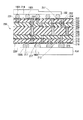
図6に第1の重複領域OL_R1の断面を示す。CPU102はプリント基板200の表面上に設けられた複数の第1パッド201にハンダボール102Aを介して実装され、ハンダボール102Aと第1パッド201とが電気的に接続される。プリント基板200の表面には第1配線層(表面配線層)202が設けられている。第1パッド201と第1配線層202の一部とは電気的に接続されている。第1パッド201および第1配線層202は、第1絶縁基板203の表面上に形成されている。
FIG. 6 shows a cross section of the first overlapping region OL_R1. The
第1絶縁基板203内に、第1パッド201または第1配線層202に接続された、第1ブラインドビア(第1の層間配線)204が設けられている。第1絶縁基板203は第2絶縁基板205の表面上に形成されている。第2絶縁基板205の表面上には第2配線層(第1の層間配線)206が形成されている。第2配線層206の一部は第1ブラインドビア204に接続されている。
A first blind via (first interlayer wiring) 204 connected to the
第2絶縁基板205内に第2配線層206の一部に接続する第1ベリードビア(第1の層間配線)207が形成されている。第2絶縁基板205は、ベース絶縁基板208の表面上に形成されている。ベース絶縁基板208上に第3配線層(第1の層間配線)209が形成されている。第3配線層209の一部は第1ベリードビア207に接続されている。ベース絶縁基板208の裏面上に第4配線層(第1の層間配線)210が形成されている。ベース絶縁基板208に第5配線層(第1の層間配線)209と第4配線層210とを接続するベースビア(第1の層間配線)211が形成されている。ベース絶縁基板208は、第3絶縁基板212の表面上に形成されている。
A first buried via (first interlayer wiring) 207 connected to a part of the
第3絶縁基板212内に第4配線層層210の一部に接続する第2ベリードビア(第1の層間配線)213が形成されている。第3絶縁基板212の裏面上に第5配線層(第1の層間配線)214が形成されている。第5配線層214の一部は第2ベリードビア213に接続されている。第3絶縁基板212は、第4絶縁基板215の表面上に形成されている。
A second buried via (first interlayer wiring) 213 connected to a part of the
第4絶縁基板215内に第2ブラインドビア(第1の層間配線)216が形成されている。第2ブラインドビア216は、第5配線層214の一部に接続されている。第4絶縁基板215の裏面上に複数の第2パッド217、および第6配線層(裏面配線層)218が形成されている。第2パッド217上にノースブリッジ104が実装されている。プリント基板200の表面側および裏面側に第1コート層219および第2コート層220が形成されている。
A second blind via (first interlayer wiring) 216 is formed in the fourth insulating
図6に示すように、第1の重複領域OL_R1内の第1パッド201の少なくとも一部と第1の重複領域OL_R1内の第2パッド217の少なくとも一部とが、第1配線層202、第1ブラインドビア204、第2配線層206、第1ベリードビア207、第3配線層209、ベースビア211、第4配線層210、第5配線層209、第2ベリードビア213、第5配線層214、第2ブラインドビア216、および第6配線層218によって電気的に接続されている。
As shown in FIG. 6, at least a part of the
また、少なくとも第1の重複領域OL_R1内において第1パッド201は、直接または第1配線層202を介して第1ブラインドビア204に接続され、スルービアに接続されていない。また、少なくとも第1の重複領域OL_R1内において、第2パッド217は、直接または第6配線層218を介して第2ブラインドビア216に接続され、スルービアに接続されていない。
In addition, at least in the first overlapping region OL_R1, the
図6に示すように、本実施形態のプリント基板200は、スタック構造である。スルービアを用いた従来のプリント基板では、ピッチの異なる2つの半導体チップの一部が重なるように両面実装することが出来ない。本実施形態のように、スタック構造のプリント基板200を用いることによって、ハンダボールの配置ピッチが異なる2つの半導体チップの一部が重なるように両面実装することができる。
As shown in FIG. 6, the printed
以下に、プリント基板200の面積を更に縮小するための構成について説明する。
Hereinafter, a configuration for further reducing the area of the printed
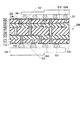
図2のブロック図に示すようにノースブリッジ104とサウスブリッジ106とが接続されている。図7に示すサウスブリッジ(第3の半導体チップ)106の裏面に二次元配列されたハンダボール106Aのハンダボール106Aの一部が、図4に示すノースブリッジ104のハンダボール104Aの一部に専用高速バスを介して電気的に接続される。 そこで、図8に示すように、サウスブリッジ106が、ノースブリッジ104に重なるプリント基板表面上の第3領域R3に実装される。ノースブリッジ104とサウスブリッジ106とを接続する高速バス(配線)を短くするために、第2領域R2と第3領域R3とが重なった第2の重複領域OL_R2内に電気的に接続されるノースブリッジ104のハンダボール104Aの少なくとも一部とサウスブリッジ106のハンダボール106Aの少なくとも一部とが配置されるようにする。第2の重複領域OL_R2内に、接続すべきハンダボール104Aの少なくとも一部とハンダボール106Aの少なくとも一部が配置されていることによって、配線長を短くすることができる。
As shown in the block diagram of FIG. 2, the
第2の重複領域OL_R2の断面を図9に示す。図9において、図6と同一な部位には同一符号を付し詳細な説明を省略する。 A cross section of the second overlapping region OL_R2 is shown in FIG. 9, parts that are the same as those in FIG. 6 are given the same reference numerals, and detailed descriptions thereof are omitted.
図9に示すように、サウスブリッジ106は、プリント基板の表面に設けられた第3パッド231にハンダボール106Aを介して接続されている。そして、第2の重複領域OL_R2内の第1パッド201の少なくとも一部と第2の重複領域OL_R2内の第3パッド217の少なくとも一部とが、第1配線層202、第1ブラインドビア204、第2配線層206、第1ベリードビア207、第3配線層209、ベースビア211、第4配線層210、第5配線層209、第2ベリードビア213、第5配線層214、第2ブラインドビア216、および第6配線層218によって電気的に接続されている。
As shown in FIG. 9, the
また、図2のブロック図に示すように、ノースブリッジ104と主メモリ114とが電気的に接続されている。主メモリ114は基板上にメモリチップが実装されたメモリモジュールで構成されている。メモリモジュールは、プリント基板200に実装されたコネクタに挿入されることによって、ノースブリッジと電気的に接続される。
Further, as shown in the block diagram of FIG. 2, the
図10に示すように、メモリモジュールが挿入されるコネクタ300は、ノースブリッジ104が配置された第2領域R2の一部に重なるプリント基板200の表面の第4領域R4に実装されている。そして、ノースブリッジ104とコネクタ300とが重なった第3の重複領域OL_R3内のノースブリッジ104のハンダボール104Aの少なくとも一部と、第3の重複領域OL_R3内のコネクタの端子の少なくとも一部とが電気的に接続される。第3の重複領域OL_R3内に、接続すべきハンダボール104Aの少なくとも一部とコネクタ300の端子の少なくとも一部が配置されていることによって、配線長を短くすることができる。
As shown in FIG. 10, the
また、図11は、発熱の大きい、CPU102およびノースブリッジ104にそれぞれ第1放熱機構401および第2放熱機構402を装着させた場合を示す図である。プリント基板200には、第1放熱機構401を取り付けるための第1の取付穴403、第2放熱機構402を取り付けるための第2の取付穴404、および第1放熱機構401および第2放熱機構402を取り付けるための第3の取付穴405が設けられている。第3の取付穴405は第1放熱機構401および第2放熱機構402を固定するための共通な取付穴となっている。このように、第1放熱機構401および第2放熱機構402を固定するための取付穴の一部を共通にすることで、デッドスペースが減り、配線エリア、実装エリアを確保することができる。
FIG. 11 is a diagram showing a case where the first
なお、本発明は、上記実施形態そのままに限定されるものではなく、実施段階ではその要旨を逸脱しない範囲で構成要素を変形して具体化できる。また、上記実施形態に開示されている複数の構成要素の適宜な組み合せにより種々の発明を形成できる。例えば、実施形態に示される全構成要素から幾つかの構成要素を削除してもよい。 Note that the present invention is not limited to the above-described embodiment as it is, and can be embodied by modifying the constituent elements without departing from the scope of the invention in the implementation stage. Further, various inventions can be formed by appropriately combining a plurality of constituent elements disclosed in the embodiment. For example, some components may be deleted from all the components shown in the embodiment.
12…コンピュータ本体,14…ディスプレイユニット,16…LCDパネル,18…ヒンジ,20…キーボード,22…マウスポイント,26…コントロールボタン,28…パワーボタン,102…CPU,102A…ハンダボール,104…ノースブリッジ,104A…ハンダボール,106…サウスブリッジ,108…グラフィクスコントローラ,112…キーボードコントローラIC,114…主メモリ,126…ハードディスクドライブ,136…BIOS−ROM,200…プリント基板,201…第1パッド,202…第1配線層,203…第1絶縁基板,204…第1ブラインドビア,205…第2絶縁基板,206…第2配線層,207…第1ベリードビア,208…ベース絶縁基板,209…第3配線層,210…第4配線層,211…インナービア,212…第3絶縁基板,213…第2ベリードビア,214…第5配線層,215…第4絶縁基板,216…第2ブラインドビア,217…第2パッド,218…第6配線層
DESCRIPTION OF
Claims (15)
前記表面上の第1領域に設けられ、第1の半導体チップの下面に配置された端子が接続可能な第1のパッドと、
前記第1領域の一部に重なった前記裏面上の第2領域に設けられ、第2の半導体チップの下面に配置された端子が接続可能な第2のパッドと、
前記第1領域と前記第2領域とが重なった重複領域内に配置された前記第1のパッドと前記重複領域内に配置された第2のパッドとを電気的に接続するための層間配線と
を具備することを特徴とするプリント基板。 A substrate body having a front surface provided with a front wiring layer and a back surface provided with a back wiring layer;
A first pad provided in a first region on the surface and connectable to a terminal disposed on a lower surface of the first semiconductor chip;
A second pad provided in a second region on the back surface that overlaps a part of the first region, to which a terminal disposed on a lower surface of the second semiconductor chip can be connected;
An interlayer wiring for electrically connecting the first pad disposed in the overlapping region where the first region and the second region overlap with the second pad disposed in the overlapping region; A printed circuit board comprising:
前記第2の領域と前記第3の領域とが重なった第2の重複領域内に配置された第2のパッドと前記第2の重複領域内に配置された第3のパッドとを接続する第2の層間配線とを更に具備することを特徴とする請求項1記載のプリント基板。 A third pad provided in a third region on the back surface overlapping with a part of the second region, to which a terminal disposed on the lower surface of the third semiconductor chip can be connected;
The second pad disposed in the second overlapping region where the second region and the third region overlap is connected to the third pad disposed in the second overlapping region. The printed circuit board according to claim 1, further comprising two interlayer wirings.
前記基板本体に設けられ、前記第2の半導体チップの表面に設けられる第2の放熱機構を取り付け可能な第2の取付穴と、
第1の放熱機構および第2の放熱機構を取り付け可能な第3の取付穴とを更に具備することを特徴とする請求項1記載のプリント基板。 A first attachment hole provided in the substrate body and capable of attaching a first heat dissipation mechanism provided on a surface of the first semiconductor chip;
A second attachment hole provided in the substrate body and capable of attaching a second heat dissipation mechanism provided on a surface of the second semiconductor chip;
The printed circuit board according to claim 1, further comprising a third mounting hole to which the first heat dissipation mechanism and the second heat dissipation mechanism can be attached.
前記第1の半導体チップは前記第1のパッドに接続され、前記第2の半導体チップは前記第2のパッドに接続されていることを特徴とする請求項1記載のプリント基板。 The first semiconductor chip and the second semiconductor chip are ball grid array type packages,
The printed circuit board according to claim 1, wherein the first semiconductor chip is connected to the first pad, and the second semiconductor chip is connected to the second pad.
第2の端子を有するブリッジ回路チップと、
表面配線層が設けられた表面と、前記表面に対向する前記裏面配線層が設けられた裏面とを有する基板本体と、
前記表面上の第1領域に設けられ、前記セントラル・プロセッシング・ユニットの前記第1の端子と接続される第1のパッドと、
前記第1領域の一部に重なった前記裏面上の第2領域に設けられ、前記ブリッジ回路チップの前記第2の端子と接続される第2のパッドと、
前記第1領域と前記第2領域とが重なった重複領域内に配置された前記第1のパッドと前記重複領域内に配置された前記第2のパッドとを電気的に接続するための層間配線と
を具備することを特徴とする情報処理装置。 A central processing unit having a first terminal;
A bridge circuit chip having a second terminal;
A substrate body having a front surface provided with a surface wiring layer and a back surface provided with the back wiring layer facing the surface;
A first pad provided in a first region on the surface and connected to the first terminal of the central processing unit;
A second pad provided in a second region on the back surface that overlaps a portion of the first region and connected to the second terminal of the bridge circuit chip;
Interlayer wiring for electrically connecting the first pad arranged in the overlapping region where the first region and the second region overlap with the second pad arranged in the overlapping region An information processing apparatus comprising:
前記第2領域の一部に重なった前記表面上の第3領域に設けられ、前記第2のブリッジ回路チップの前記第3の端子と接続される第3のパッドと、
前記第2の領域と前記第3の領域とが重なった第2の重複領域内に配置された第2のパッドと前記第2の重複領域内に配置された第3のパッドとを接続する第2の層間配線とを更に具備することを特徴とする請求項8記載の情報処理装置。 A second bridge circuit chip having a third terminal;
A third pad provided in a third region on the surface overlying a portion of the second region and connected to the third terminal of the second bridge circuit chip;
The second pad disposed in the second overlapping region where the second region and the third region overlap each other and the third pad disposed in the second overlapping region are connected to each other. 9. The information processing apparatus according to claim 8, further comprising two interlayer wirings.
前記第2の半導体チップの表面に設けられた第2の放熱機構とを更に具備し、
前記基板本体は、前記第1の放熱機構を取り付けるための第1の取付穴と、前記第2の放熱機構を取り付けるための第2の取付穴と、前記第1の放熱機構および第2の放熱機構を取り付けるための第3の取付穴とを有することを特徴とする請求項8記載の情報処理装置。 A first heat dissipation mechanism provided on the surface of the first semiconductor chip;
A second heat dissipating mechanism provided on the surface of the second semiconductor chip,
The substrate body includes a first mounting hole for mounting the first heat dissipation mechanism, a second mounting hole for mounting the second heat dissipation mechanism, the first heat dissipation mechanism and the second heat dissipation mechanism. The information processing apparatus according to claim 8, further comprising a third mounting hole for mounting the mechanism.
Priority Applications (3)
| Application Number | Priority Date | Filing Date | Title |
|---|---|---|---|
| JP2005119579A JP2006303003A (en) | 2005-04-18 | 2005-04-18 | Printed circuit board and information processing apparatus |
| US11/404,771 US7453704B2 (en) | 2005-04-18 | 2006-04-17 | Printed wiring board and information processing apparatus |
| US12/168,508 US20080271914A1 (en) | 2005-04-18 | 2008-07-07 | Printed wiring board and information processing apparatus |
Applications Claiming Priority (1)
| Application Number | Priority Date | Filing Date | Title |
|---|---|---|---|
| JP2005119579A JP2006303003A (en) | 2005-04-18 | 2005-04-18 | Printed circuit board and information processing apparatus |
Publications (1)
| Publication Number | Publication Date |
|---|---|
| JP2006303003A true JP2006303003A (en) | 2006-11-02 |
Family
ID=37107708
Family Applications (1)
| Application Number | Title | Priority Date | Filing Date |
|---|---|---|---|
| JP2005119579A Pending JP2006303003A (en) | 2005-04-18 | 2005-04-18 | Printed circuit board and information processing apparatus |
Country Status (2)
| Country | Link |
|---|---|
| US (2) | US7453704B2 (en) |
| JP (1) | JP2006303003A (en) |
Cited By (3)
| Publication number | Priority date | Publication date | Assignee | Title |
|---|---|---|---|---|
| JP2008159897A (en) * | 2006-12-25 | 2008-07-10 | Elpida Memory Inc | Multilayer printed circuit board |
| KR20140030717A (en) * | 2012-09-03 | 2014-03-12 | 삼성전자주식회사 | Electronic apparatus, method for optimize of de-coupling capacitor and computer-readable recording medium |
| JP2015179795A (en) * | 2013-05-30 | 2015-10-08 | 京セラサーキットソリューションズ株式会社 | Wiring board |
Families Citing this family (5)
| Publication number | Priority date | Publication date | Assignee | Title |
|---|---|---|---|---|
| TWI380427B (en) * | 2007-01-16 | 2012-12-21 | Advanced Semiconductor Eng | Substrate and the semiconductor package comprising the same |
| US8674235B2 (en) * | 2011-06-06 | 2014-03-18 | Intel Corporation | Microelectronic substrate for alternate package functionality |
| JP2014229761A (en) * | 2013-05-23 | 2014-12-08 | 株式会社東芝 | Electronic apparatus |
| KR102287396B1 (en) * | 2014-10-21 | 2021-08-06 | 삼성전자주식회사 | SYSTEM ON PACKAGE (SoP) MODULE AND MOBILE COMPUTING DEVICE HAVING THE SoP |
| US9832876B2 (en) * | 2014-12-18 | 2017-11-28 | Intel Corporation | CPU package substrates with removable memory mechanical interfaces |
Citations (4)
| Publication number | Priority date | Publication date | Assignee | Title |
|---|---|---|---|---|
| JPH0360218A (en) * | 1989-07-28 | 1991-03-15 | Toshiba Corp | Semiconductor integrated circuit |
| JPH11154728A (en) * | 1997-09-16 | 1999-06-08 | Matsushita Electric Ind Co Ltd | Semiconductor device and its mounted body |
| JP2001024150A (en) * | 1999-07-06 | 2001-01-26 | Sony Corp | Semiconductor device |
| JP2002009445A (en) * | 2000-06-21 | 2002-01-11 | Sumitomo Metal Electronics Devices Inc | Electronic equipment |
Family Cites Families (14)
| Publication number | Priority date | Publication date | Assignee | Title |
|---|---|---|---|---|
| US6545875B1 (en) * | 2000-05-10 | 2003-04-08 | Rambus, Inc. | Multiple channel modules and bus systems using same |
| JP2001339037A (en) | 2000-05-26 | 2001-12-07 | Matsushita Electric Ind Co Ltd | Semiconductor element mounting structure |
| US6734539B2 (en) * | 2000-12-27 | 2004-05-11 | Lucent Technologies Inc. | Stacked module package |
| JP2003218505A (en) | 2002-01-17 | 2003-07-31 | Matsushita Electric Ind Co Ltd | Printed circuit board, printed circuit board unit, method of inspecting and manufacturing printed circuit board unit, and communication device using printed circuit board unit |
| JP3994379B2 (en) * | 2002-03-25 | 2007-10-17 | 株式会社リコー | Wiring layout structure of auxiliary package for wiring and printed circuit wiring board |
| JP3956204B2 (en) * | 2002-06-27 | 2007-08-08 | 日本特殊陶業株式会社 | MULTILAYER RESIN WIRING BOARD AND METHOD FOR MANUFACTURING THE SAME, METAL PLATE FOR LAMINATED RESIN WIRING BOARD |
| US7294928B2 (en) * | 2002-09-06 | 2007-11-13 | Tessera, Inc. | Components, methods and assemblies for stacked packages |
| US7034387B2 (en) * | 2003-04-04 | 2006-04-25 | Chippac, Inc. | Semiconductor multipackage module including processor and memory package assemblies |
| US6885541B2 (en) * | 2003-06-20 | 2005-04-26 | Ngk Spark Plug Co., Ltd. | Capacitor, and capacitor manufacturing process |
| US6958538B1 (en) * | 2003-09-26 | 2005-10-25 | Sun Microsystems, Inc. | Computer system architecture using a proximity I/O switch |
| US6982481B1 (en) * | 2003-10-08 | 2006-01-03 | Nortel Networks Limited | System for dissipating heat and shielding electromagnetic radiation produced by an electronic device |
| JP4738996B2 (en) * | 2004-12-13 | 2011-08-03 | キヤノン株式会社 | Semiconductor device |
| US7269025B2 (en) * | 2004-12-30 | 2007-09-11 | Intel Corporation | Ballout for buffer |
| US7978479B2 (en) * | 2007-08-15 | 2011-07-12 | Accton Technology Corporation | WLAN SiP module |
-
2005
- 2005-04-18 JP JP2005119579A patent/JP2006303003A/en active Pending
-
2006
- 2006-04-17 US US11/404,771 patent/US7453704B2/en not_active Expired - Fee Related
-
2008
- 2008-07-07 US US12/168,508 patent/US20080271914A1/en not_active Abandoned
Patent Citations (4)
| Publication number | Priority date | Publication date | Assignee | Title |
|---|---|---|---|---|
| JPH0360218A (en) * | 1989-07-28 | 1991-03-15 | Toshiba Corp | Semiconductor integrated circuit |
| JPH11154728A (en) * | 1997-09-16 | 1999-06-08 | Matsushita Electric Ind Co Ltd | Semiconductor device and its mounted body |
| JP2001024150A (en) * | 1999-07-06 | 2001-01-26 | Sony Corp | Semiconductor device |
| JP2002009445A (en) * | 2000-06-21 | 2002-01-11 | Sumitomo Metal Electronics Devices Inc | Electronic equipment |
Cited By (5)
| Publication number | Priority date | Publication date | Assignee | Title |
|---|---|---|---|---|
| JP2008159897A (en) * | 2006-12-25 | 2008-07-10 | Elpida Memory Inc | Multilayer printed circuit board |
| US8198549B2 (en) | 2006-12-25 | 2012-06-12 | Elpida Memory, Inc. | Multi-layer printed wiring board |
| KR20140030717A (en) * | 2012-09-03 | 2014-03-12 | 삼성전자주식회사 | Electronic apparatus, method for optimize of de-coupling capacitor and computer-readable recording medium |
| KR101869303B1 (en) * | 2012-09-03 | 2018-06-20 | 에이치피프린팅코리아 주식회사 | Electronic apparatus, method for optimize of de-coupling capacitor and computer-readable recording medium |
| JP2015179795A (en) * | 2013-05-30 | 2015-10-08 | 京セラサーキットソリューションズ株式会社 | Wiring board |
Also Published As
| Publication number | Publication date |
|---|---|
| US7453704B2 (en) | 2008-11-18 |
| US20060231912A1 (en) | 2006-10-19 |
| US20080271914A1 (en) | 2008-11-06 |
Similar Documents
| Publication | Publication Date | Title |
|---|---|---|
| US20080271914A1 (en) | Printed wiring board and information processing apparatus | |
| US20080130234A1 (en) | Electronic Apparatus | |
| US7345359B2 (en) | Integrated circuit package with chip-side signal connections | |
| EP3300466A1 (en) | Narrow border displays for electronic devices | |
| US20080296047A1 (en) | Printed wiring board assembly, method of mounting components on printed wiring board and electronic apparatus | |
| KR101124548B1 (en) | Printed substrate and electronic device | |
| JP2005166715A (en) | Electronics | |
| CN101277582A (en) | Printed Circuit Boards and Electronics | |
| JPH11289142A (en) | Circuit module mounting structure and electronic device having this circuit module | |
| JP2009134932A (en) | Electronic equipment and printed circuit board unit | |
| US7957157B2 (en) | Printed circuit board | |
| JP5657232B2 (en) | Semiconductor package | |
| JP2007273564A (en) | Printed circuit boards, semiconductor packages, and electronic equipment | |
| US7593232B2 (en) | Electronic apparatus and circuit board unit | |
| JP2002289764A (en) | Flexible circuit board, display device and electronic device using the same | |
| US7167374B2 (en) | Circuit substrate and electronic equipment | |
| JP2013118296A (en) | Electronic apparatus | |
| JP2009076634A (en) | Double-sided flexible board with heat conduction design | |
| JP2008084019A (en) | Electronic device | |
| JPH10189867A (en) | Circuit module and portable electronic device containing this circuit module | |
| JP2002009197A (en) | Semiconductor device and wiring method inside package thereof | |
| JP2006270930A (en) | Mobile device | |
| JPH11112121A (en) | Circuit module and electronic equipment incorporating circuit module | |
| TWI914867B (en) | Method of using optimized pitch for installing processing circuit at printed circuit board, and associated apparatus | |
| JP2010093310A (en) | Electronic apparatus |
Legal Events
| Date | Code | Title | Description |
|---|---|---|---|
| A621 | Written request for application examination |
Free format text: JAPANESE INTERMEDIATE CODE: A621 Effective date: 20080313 |
|
| A977 | Report on retrieval |
Free format text: JAPANESE INTERMEDIATE CODE: A971007 Effective date: 20100930 |
|
| A131 | Notification of reasons for refusal |
Free format text: JAPANESE INTERMEDIATE CODE: A131 Effective date: 20101005 |
|
| A521 | Request for written amendment filed |
Free format text: JAPANESE INTERMEDIATE CODE: A523 Effective date: 20101206 |
|
| A02 | Decision of refusal |
Free format text: JAPANESE INTERMEDIATE CODE: A02 Effective date: 20110222 |