JP2006303003A - プリント基板、および情報処理装置 - Google Patents
プリント基板、および情報処理装置 Download PDFInfo
- Publication number
- JP2006303003A JP2006303003A JP2005119579A JP2005119579A JP2006303003A JP 2006303003 A JP2006303003 A JP 2006303003A JP 2005119579 A JP2005119579 A JP 2005119579A JP 2005119579 A JP2005119579 A JP 2005119579A JP 2006303003 A JP2006303003 A JP 2006303003A
- Authority
- JP
- Japan
- Prior art keywords
- region
- pad
- semiconductor chip
- printed circuit
- circuit board
- Prior art date
- Legal status (The legal status is an assumption and is not a legal conclusion. Google has not performed a legal analysis and makes no representation as to the accuracy of the status listed.)
- Pending
Links
Images






Classifications
-
- G—PHYSICS
- G06—COMPUTING OR CALCULATING; COUNTING
- G06F—ELECTRIC DIGITAL DATA PROCESSING
- G06F1/00—Details not covered by groups G06F3/00 - G06F13/00 and G06F21/00
- G06F1/16—Constructional details or arrangements
- G06F1/1613—Constructional details or arrangements for portable computers
- G06F1/1615—Constructional details or arrangements for portable computers with several enclosures having relative motions, each enclosure supporting at least one I/O or computing function
- G06F1/1616—Constructional details or arrangements for portable computers with several enclosures having relative motions, each enclosure supporting at least one I/O or computing function with folding flat displays, e.g. laptop computers or notebooks having a clamshell configuration, with body parts pivoting to an open position around an axis parallel to the plane they define in closed position
-
- G—PHYSICS
- G06—COMPUTING OR CALCULATING; COUNTING
- G06F—ELECTRIC DIGITAL DATA PROCESSING
- G06F1/00—Details not covered by groups G06F3/00 - G06F13/00 and G06F21/00
- G06F1/16—Constructional details or arrangements
- G06F1/1613—Constructional details or arrangements for portable computers
- G06F1/1633—Constructional details or arrangements of portable computers not specific to the type of enclosures covered by groups G06F1/1615 - G06F1/1626
- G06F1/1656—Details related to functional adaptations of the enclosure, e.g. to provide protection against EMI, shock, water, or to host detachable peripherals like a mouse or removable expansions units like PCMCIA cards, or to provide access to internal components for maintenance or to removable storage supports like CDs or DVDs, or to mechanically mount accessories
-
- G—PHYSICS
- G06—COMPUTING OR CALCULATING; COUNTING
- G06F—ELECTRIC DIGITAL DATA PROCESSING
- G06F1/00—Details not covered by groups G06F3/00 - G06F13/00 and G06F21/00
- G06F1/16—Constructional details or arrangements
- G06F1/18—Packaging or power distribution
-
- H—ELECTRICITY
- H05—ELECTRIC TECHNIQUES NOT OTHERWISE PROVIDED FOR
- H05K—PRINTED CIRCUITS; CASINGS OR CONSTRUCTIONAL DETAILS OF ELECTRIC APPARATUS; MANUFACTURE OF ASSEMBLAGES OF ELECTRICAL COMPONENTS
- H05K1/00—Printed circuits
- H05K1/18—Printed circuits structurally associated with non-printed electric components
- H05K1/181—Printed circuits structurally associated with non-printed electric components associated with surface mounted components
-
- H—ELECTRICITY
- H05—ELECTRIC TECHNIQUES NOT OTHERWISE PROVIDED FOR
- H05K—PRINTED CIRCUITS; CASINGS OR CONSTRUCTIONAL DETAILS OF ELECTRIC APPARATUS; MANUFACTURE OF ASSEMBLAGES OF ELECTRICAL COMPONENTS
- H05K1/00—Printed circuits
- H05K1/02—Details
- H05K1/11—Printed elements for providing electric connections to or between printed circuits
- H05K1/111—Pads for surface mounting, e.g. lay-out
- H05K1/112—Pads for surface mounting, e.g. lay-out directly combined with via connections
- H05K1/114—Pad being close to via, but not surrounding the via
-
- H—ELECTRICITY
- H05—ELECTRIC TECHNIQUES NOT OTHERWISE PROVIDED FOR
- H05K—PRINTED CIRCUITS; CASINGS OR CONSTRUCTIONAL DETAILS OF ELECTRIC APPARATUS; MANUFACTURE OF ASSEMBLAGES OF ELECTRICAL COMPONENTS
- H05K2201/00—Indexing scheme relating to printed circuits covered by H05K1/00
- H05K2201/09—Shape and layout
- H05K2201/09209—Shape and layout details of conductors
- H05K2201/095—Conductive through-holes or vias
- H05K2201/09536—Buried plated through-holes, i.e. plated through-holes formed in a core before lamination
-
- H—ELECTRICITY
- H05—ELECTRIC TECHNIQUES NOT OTHERWISE PROVIDED FOR
- H05K—PRINTED CIRCUITS; CASINGS OR CONSTRUCTIONAL DETAILS OF ELECTRIC APPARATUS; MANUFACTURE OF ASSEMBLAGES OF ELECTRICAL COMPONENTS
- H05K2201/00—Indexing scheme relating to printed circuits covered by H05K1/00
- H05K2201/09—Shape and layout
- H05K2201/09209—Shape and layout details of conductors
- H05K2201/095—Conductive through-holes or vias
- H05K2201/096—Vertically aligned vias, holes or stacked vias
-
- H—ELECTRICITY
- H05—ELECTRIC TECHNIQUES NOT OTHERWISE PROVIDED FOR
- H05K—PRINTED CIRCUITS; CASINGS OR CONSTRUCTIONAL DETAILS OF ELECTRIC APPARATUS; MANUFACTURE OF ASSEMBLAGES OF ELECTRICAL COMPONENTS
- H05K2201/00—Indexing scheme relating to printed circuits covered by H05K1/00
- H05K2201/09—Shape and layout
- H05K2201/09209—Shape and layout details of conductors
- H05K2201/095—Conductive through-holes or vias
- H05K2201/09627—Special connections between adjacent vias, not for grounding vias
-
- H—ELECTRICITY
- H05—ELECTRIC TECHNIQUES NOT OTHERWISE PROVIDED FOR
- H05K—PRINTED CIRCUITS; CASINGS OR CONSTRUCTIONAL DETAILS OF ELECTRIC APPARATUS; MANUFACTURE OF ASSEMBLAGES OF ELECTRICAL COMPONENTS
- H05K2201/00—Indexing scheme relating to printed circuits covered by H05K1/00
- H05K2201/10—Details of components or other objects attached to or integrated in a printed circuit board
- H05K2201/10007—Types of components
- H05K2201/10189—Non-printed connector
-
- H—ELECTRICITY
- H05—ELECTRIC TECHNIQUES NOT OTHERWISE PROVIDED FOR
- H05K—PRINTED CIRCUITS; CASINGS OR CONSTRUCTIONAL DETAILS OF ELECTRIC APPARATUS; MANUFACTURE OF ASSEMBLAGES OF ELECTRICAL COMPONENTS
- H05K2201/00—Indexing scheme relating to printed circuits covered by H05K1/00
- H05K2201/10—Details of components or other objects attached to or integrated in a printed circuit board
- H05K2201/10431—Details of mounted components
- H05K2201/10507—Involving several components
- H05K2201/10545—Related components mounted on both sides of the PCB
-
- H—ELECTRICITY
- H05—ELECTRIC TECHNIQUES NOT OTHERWISE PROVIDED FOR
- H05K—PRINTED CIRCUITS; CASINGS OR CONSTRUCTIONAL DETAILS OF ELECTRIC APPARATUS; MANUFACTURE OF ASSEMBLAGES OF ELECTRICAL COMPONENTS
- H05K2201/00—Indexing scheme relating to printed circuits covered by H05K1/00
- H05K2201/10—Details of components or other objects attached to or integrated in a printed circuit board
- H05K2201/10613—Details of electrical connections of non-printed components, e.g. special leads
- H05K2201/10621—Components characterised by their electrical contacts
- H05K2201/10734—Ball grid array [BGA]; Bump grid array
-
- H—ELECTRICITY
- H05—ELECTRIC TECHNIQUES NOT OTHERWISE PROVIDED FOR
- H05K—PRINTED CIRCUITS; CASINGS OR CONSTRUCTIONAL DETAILS OF ELECTRIC APPARATUS; MANUFACTURE OF ASSEMBLAGES OF ELECTRICAL COMPONENTS
- H05K2203/00—Indexing scheme relating to apparatus or processes for manufacturing printed circuits covered by H05K3/00
- H05K2203/15—Position of the PCB during processing
- H05K2203/1572—Processing both sides of a PCB by the same process; Providing a similar arrangement of components on both sides; Making interlayer connections from two sides
-
- H—ELECTRICITY
- H05—ELECTRIC TECHNIQUES NOT OTHERWISE PROVIDED FOR
- H05K—PRINTED CIRCUITS; CASINGS OR CONSTRUCTIONAL DETAILS OF ELECTRIC APPARATUS; MANUFACTURE OF ASSEMBLAGES OF ELECTRICAL COMPONENTS
- H05K3/00—Apparatus or processes for manufacturing printed circuits
- H05K3/46—Manufacturing multilayer circuits
- H05K3/4602—Manufacturing multilayer circuits characterized by a special circuit board as base or central core whereon additional circuit layers are built or additional circuit boards are laminated
-
- H—ELECTRICITY
- H10—SEMICONDUCTOR DEVICES; ELECTRIC SOLID-STATE DEVICES NOT OTHERWISE PROVIDED FOR
- H10W—GENERIC PACKAGES, INTERCONNECTIONS, CONNECTORS OR OTHER CONSTRUCTIONAL DETAILS OF DEVICES COVERED BY CLASS H10
- H10W90/00—Package configurations
- H10W90/701—Package configurations characterised by the relative positions of pads or connectors relative to package parts
- H10W90/721—Package configurations characterised by the relative positions of pads or connectors relative to package parts of bump connectors
- H10W90/724—Package configurations characterised by the relative positions of pads or connectors relative to package parts of bump connectors between a chip and a stacked insulating package substrate, interposer or RDL
-
- Y—GENERAL TAGGING OF NEW TECHNOLOGICAL DEVELOPMENTS; GENERAL TAGGING OF CROSS-SECTIONAL TECHNOLOGIES SPANNING OVER SEVERAL SECTIONS OF THE IPC; TECHNICAL SUBJECTS COVERED BY FORMER USPC CROSS-REFERENCE ART COLLECTIONS [XRACs] AND DIGESTS
- Y02—TECHNOLOGIES OR APPLICATIONS FOR MITIGATION OR ADAPTATION AGAINST CLIMATE CHANGE
- Y02P—CLIMATE CHANGE MITIGATION TECHNOLOGIES IN THE PRODUCTION OR PROCESSING OF GOODS
- Y02P70/00—Climate change mitigation technologies in the production process for final industrial or consumer products
- Y02P70/50—Manufacturing or production processes characterised by the final manufactured product
Landscapes
- Engineering & Computer Science (AREA)
- Theoretical Computer Science (AREA)
- Computer Hardware Design (AREA)
- Physics & Mathematics (AREA)
- General Engineering & Computer Science (AREA)
- Human Computer Interaction (AREA)
- General Physics & Mathematics (AREA)
- Mathematical Physics (AREA)
- Power Engineering (AREA)
- Microelectronics & Electronic Packaging (AREA)
- Combinations Of Printed Boards (AREA)
- Structures For Mounting Electric Components On Printed Circuit Boards (AREA)
- Production Of Multi-Layered Print Wiring Board (AREA)
- Structure Of Printed Boards (AREA)
Abstract
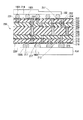
【解決手段】第1の重複領域OL_R1内の第1パッド201の少なくとも一部と第1の重複領域OL_R1内の第2パッド217の少なくとも一部とが、第1配線層202、第1ブラインドビア204、第2配線層206、第1ベリードビア207、第3配線層209、ベースビア211、第4配線層210、第5配線層209、第2ベリードビア213、第5配線層214、第2ブラインドビア216、および第6配線層218によって電気的に接続されている。少なくとも第1の重複領域OL_R1内において第1パッド201は、直接または第1配線層202を介して第1ブラインドビア204に接続され、スルービアに接続されていない。また、少なくとも第1の重複領域OL_R1内において、第2パッド217は、直接または第6配線層218を介して第2ブラインドビア216に接続され、スルービアに接続されていない。
【選択図】 図6
Description
Claims (15)
- 表面配線層が設けられた表面と、裏面配線層が設けられた裏面とを有する基板本体と、
前記表面上の第1領域に設けられ、第1の半導体チップの下面に配置された端子が接続可能な第1のパッドと、
前記第1領域の一部に重なった前記裏面上の第2領域に設けられ、第2の半導体チップの下面に配置された端子が接続可能な第2のパッドと、
前記第1領域と前記第2領域とが重なった重複領域内に配置された前記第1のパッドと前記重複領域内に配置された第2のパッドとを電気的に接続するための層間配線と
を具備することを特徴とするプリント基板。 - 第1の半導体チップの下面に設けられた端子の配置ピッチと、第2の半導体チップの下面に設けられた端子の配置ピッチとが異なることを特徴とする請求項1記載のプリント基板。
- 前記重複領域内で、前記第1のパッド、および前記第2のパッドに接続する第1の層間配線は、ブラインドビアであることを特徴とする請求項1記載のプリント基板。
- 前記第2領域の一部に重なった前記裏面上の第3領域に設けられ、第3の半導体チップの下面に配置された端子が接続可能な第3のパッドと、
前記第2の領域と前記第3の領域とが重なった第2の重複領域内に配置された第2のパッドと前記第2の重複領域内に配置された第3のパッドとを接続する第2の層間配線とを更に具備することを特徴とする請求項1記載のプリント基板。 - 前記第2領域の一部に重なった前記裏面上の第4領域に設けられ、第4の半導体チップが実装された基板を挿入するためのコネクタを更に具備することを特徴とする請求項1記載のプリント基板。
- 前記基板本体に設けられ、前記第1の半導体チップの表面に設けられる第1の放熱機構を取り付け可能な第1の取付穴と、
前記基板本体に設けられ、前記第2の半導体チップの表面に設けられる第2の放熱機構を取り付け可能な第2の取付穴と、
第1の放熱機構および第2の放熱機構を取り付け可能な第3の取付穴とを更に具備することを特徴とする請求項1記載のプリント基板。 - 前記第1の半導体チップおよび前記第2の半導体チップは、ボール・グリッド・アレイ型のパッケージであって、
前記第1の半導体チップは前記第1のパッドに接続され、前記第2の半導体チップは前記第2のパッドに接続されていることを特徴とする請求項1記載のプリント基板。 - 第1の端子を有するセントラル・プロセッシング・ユニットと、
第2の端子を有するブリッジ回路チップと、
表面配線層が設けられた表面と、前記表面に対向する前記裏面配線層が設けられた裏面とを有する基板本体と、
前記表面上の第1領域に設けられ、前記セントラル・プロセッシング・ユニットの前記第1の端子と接続される第1のパッドと、
前記第1領域の一部に重なった前記裏面上の第2領域に設けられ、前記ブリッジ回路チップの前記第2の端子と接続される第2のパッドと、
前記第1領域と前記第2領域とが重なった重複領域内に配置された前記第1のパッドと前記重複領域内に配置された前記第2のパッドとを電気的に接続するための層間配線と
を具備することを特徴とする情報処理装置。 - 前記第1の端子の配置ピッチと、前記第2の端子の配置ピッチとが異なることを特徴とする請求項8記載の情報処理装置。
- 前記基板本体はスタック構造を有することを特徴とする請求項8記載の情報処理装置。
- 前記重複領域内で、前記第1のパッド、および前記第2のパッドに接続する第1の層間配線は、ブラインドビアであることを特徴とする請求項8記載の情報処理装置。
- 第3の端子を有する第2のブリッジ回路チップと、
前記第2領域の一部に重なった前記表面上の第3領域に設けられ、前記第2のブリッジ回路チップの前記第3の端子と接続される第3のパッドと、
前記第2の領域と前記第3の領域とが重なった第2の重複領域内に配置された第2のパッドと前記第2の重複領域内に配置された第3のパッドとを接続する第2の層間配線とを更に具備することを特徴とする請求項8記載の情報処理装置。 - 前記第2領域の一部に重なった前記表面上の第4領域に設けられ、メモリモジュールを挿入するためのコネクタを更に具備することを特徴とする請求項8記載の情報処理装置。
- 前記第1の半導体チップの表面に設けられた第1の放熱機構と、
前記第2の半導体チップの表面に設けられた第2の放熱機構とを更に具備し、
前記基板本体は、前記第1の放熱機構を取り付けるための第1の取付穴と、前記第2の放熱機構を取り付けるための第2の取付穴と、前記第1の放熱機構および第2の放熱機構を取り付けるための第3の取付穴とを有することを特徴とする請求項8記載の情報処理装置。 - 前記第1の半導体チップおよび前記第2の半導体チップは、ボール・グリッド・アレイ型のパッケージであることを特徴とする請求項8記載の情報処理装置。
Priority Applications (3)
| Application Number | Priority Date | Filing Date | Title |
|---|---|---|---|
| JP2005119579A JP2006303003A (ja) | 2005-04-18 | 2005-04-18 | プリント基板、および情報処理装置 |
| US11/404,771 US7453704B2 (en) | 2005-04-18 | 2006-04-17 | Printed wiring board and information processing apparatus |
| US12/168,508 US20080271914A1 (en) | 2005-04-18 | 2008-07-07 | Printed wiring board and information processing apparatus |
Applications Claiming Priority (1)
| Application Number | Priority Date | Filing Date | Title |
|---|---|---|---|
| JP2005119579A JP2006303003A (ja) | 2005-04-18 | 2005-04-18 | プリント基板、および情報処理装置 |
Publications (1)
| Publication Number | Publication Date |
|---|---|
| JP2006303003A true JP2006303003A (ja) | 2006-11-02 |
Family
ID=37107708
Family Applications (1)
| Application Number | Title | Priority Date | Filing Date |
|---|---|---|---|
| JP2005119579A Pending JP2006303003A (ja) | 2005-04-18 | 2005-04-18 | プリント基板、および情報処理装置 |
Country Status (2)
| Country | Link |
|---|---|
| US (2) | US7453704B2 (ja) |
| JP (1) | JP2006303003A (ja) |
Cited By (3)
| Publication number | Priority date | Publication date | Assignee | Title |
|---|---|---|---|---|
| JP2008159897A (ja) * | 2006-12-25 | 2008-07-10 | Elpida Memory Inc | 多層プリント配線板 |
| KR20140030717A (ko) * | 2012-09-03 | 2014-03-12 | 삼성전자주식회사 | 전자 장치, 디-커플링 커패시터 최적화 방법 및 컴퓨터 판독가능 기록매체 |
| JP2015179795A (ja) * | 2013-05-30 | 2015-10-08 | 京セラサーキットソリューションズ株式会社 | 配線基板 |
Families Citing this family (5)
| Publication number | Priority date | Publication date | Assignee | Title |
|---|---|---|---|---|
| TWI380427B (en) * | 2007-01-16 | 2012-12-21 | Advanced Semiconductor Eng | Substrate and the semiconductor package comprising the same |
| US8674235B2 (en) * | 2011-06-06 | 2014-03-18 | Intel Corporation | Microelectronic substrate for alternate package functionality |
| JP2014229761A (ja) * | 2013-05-23 | 2014-12-08 | 株式会社東芝 | 電子機器 |
| KR102287396B1 (ko) * | 2014-10-21 | 2021-08-06 | 삼성전자주식회사 | 시스템 온 패키지 모듈과 이를 포함하는 모바일 컴퓨팅 장치 |
| US9832876B2 (en) * | 2014-12-18 | 2017-11-28 | Intel Corporation | CPU package substrates with removable memory mechanical interfaces |
Citations (4)
| Publication number | Priority date | Publication date | Assignee | Title |
|---|---|---|---|---|
| JPH0360218A (ja) * | 1989-07-28 | 1991-03-15 | Toshiba Corp | 半導体集積回路 |
| JPH11154728A (ja) * | 1997-09-16 | 1999-06-08 | Matsushita Electric Ind Co Ltd | 半導体装置およびその実装体 |
| JP2001024150A (ja) * | 1999-07-06 | 2001-01-26 | Sony Corp | 半導体装置 |
| JP2002009445A (ja) * | 2000-06-21 | 2002-01-11 | Sumitomo Metal Electronics Devices Inc | 電子装置 |
Family Cites Families (14)
| Publication number | Priority date | Publication date | Assignee | Title |
|---|---|---|---|---|
| US6545875B1 (en) * | 2000-05-10 | 2003-04-08 | Rambus, Inc. | Multiple channel modules and bus systems using same |
| JP2001339037A (ja) | 2000-05-26 | 2001-12-07 | Matsushita Electric Ind Co Ltd | 半導体素子の実装構造体 |
| US6734539B2 (en) * | 2000-12-27 | 2004-05-11 | Lucent Technologies Inc. | Stacked module package |
| JP2003218505A (ja) | 2002-01-17 | 2003-07-31 | Matsushita Electric Ind Co Ltd | プリント基板とプリント基板ユニット及びプリント基板ユニットの検査方法と製造方法並びにプリント基板ユニットを使用した通信機器 |
| JP3994379B2 (ja) | 2002-03-25 | 2007-10-17 | 株式会社リコー | 配線用補助パッケージおよび印刷回路配線板の配線レイアウト構造 |
| JP3956204B2 (ja) * | 2002-06-27 | 2007-08-08 | 日本特殊陶業株式会社 | 積層樹脂配線基板及びその製造方法、積層樹脂配線基板用金属板 |
| US7294928B2 (en) * | 2002-09-06 | 2007-11-13 | Tessera, Inc. | Components, methods and assemblies for stacked packages |
| US7034387B2 (en) * | 2003-04-04 | 2006-04-25 | Chippac, Inc. | Semiconductor multipackage module including processor and memory package assemblies |
| US6885541B2 (en) * | 2003-06-20 | 2005-04-26 | Ngk Spark Plug Co., Ltd. | Capacitor, and capacitor manufacturing process |
| US6958538B1 (en) * | 2003-09-26 | 2005-10-25 | Sun Microsystems, Inc. | Computer system architecture using a proximity I/O switch |
| US6982481B1 (en) * | 2003-10-08 | 2006-01-03 | Nortel Networks Limited | System for dissipating heat and shielding electromagnetic radiation produced by an electronic device |
| JP4738996B2 (ja) * | 2004-12-13 | 2011-08-03 | キヤノン株式会社 | 半導体装置 |
| US7269025B2 (en) * | 2004-12-30 | 2007-09-11 | Intel Corporation | Ballout for buffer |
| US7978479B2 (en) * | 2007-08-15 | 2011-07-12 | Accton Technology Corporation | WLAN SiP module |
-
2005
- 2005-04-18 JP JP2005119579A patent/JP2006303003A/ja active Pending
-
2006
- 2006-04-17 US US11/404,771 patent/US7453704B2/en not_active Expired - Fee Related
-
2008
- 2008-07-07 US US12/168,508 patent/US20080271914A1/en not_active Abandoned
Patent Citations (4)
| Publication number | Priority date | Publication date | Assignee | Title |
|---|---|---|---|---|
| JPH0360218A (ja) * | 1989-07-28 | 1991-03-15 | Toshiba Corp | 半導体集積回路 |
| JPH11154728A (ja) * | 1997-09-16 | 1999-06-08 | Matsushita Electric Ind Co Ltd | 半導体装置およびその実装体 |
| JP2001024150A (ja) * | 1999-07-06 | 2001-01-26 | Sony Corp | 半導体装置 |
| JP2002009445A (ja) * | 2000-06-21 | 2002-01-11 | Sumitomo Metal Electronics Devices Inc | 電子装置 |
Cited By (5)
| Publication number | Priority date | Publication date | Assignee | Title |
|---|---|---|---|---|
| JP2008159897A (ja) * | 2006-12-25 | 2008-07-10 | Elpida Memory Inc | 多層プリント配線板 |
| US8198549B2 (en) | 2006-12-25 | 2012-06-12 | Elpida Memory, Inc. | Multi-layer printed wiring board |
| KR20140030717A (ko) * | 2012-09-03 | 2014-03-12 | 삼성전자주식회사 | 전자 장치, 디-커플링 커패시터 최적화 방법 및 컴퓨터 판독가능 기록매체 |
| KR101869303B1 (ko) * | 2012-09-03 | 2018-06-20 | 에이치피프린팅코리아 주식회사 | 전자 장치, 디-커플링 커패시터 최적화 방법 및 컴퓨터 판독가능 기록매체 |
| JP2015179795A (ja) * | 2013-05-30 | 2015-10-08 | 京セラサーキットソリューションズ株式会社 | 配線基板 |
Also Published As
| Publication number | Publication date |
|---|---|
| US7453704B2 (en) | 2008-11-18 |
| US20080271914A1 (en) | 2008-11-06 |
| US20060231912A1 (en) | 2006-10-19 |
Similar Documents
| Publication | Publication Date | Title |
|---|---|---|
| US20080271914A1 (en) | Printed wiring board and information processing apparatus | |
| US20080130234A1 (en) | Electronic Apparatus | |
| US7345359B2 (en) | Integrated circuit package with chip-side signal connections | |
| EP3300466A1 (en) | Narrow border displays for electronic devices | |
| US20080296047A1 (en) | Printed wiring board assembly, method of mounting components on printed wiring board and electronic apparatus | |
| KR101124548B1 (ko) | 프린트 기판 및 전자 기기 | |
| JP2005166715A (ja) | 電子機器 | |
| CN101277582A (zh) | 印刷电路板和电子设备 | |
| US7269025B2 (en) | Ballout for buffer | |
| JPH11289142A (ja) | 回路モジュール実装構造およびこの回路モジュールを有する電子機器 | |
| JP2009134932A (ja) | 電子機器およびプリント基板ユニット | |
| US7957157B2 (en) | Printed circuit board | |
| JP5657232B2 (ja) | 半導体パッケージ | |
| JP2007273564A (ja) | プリント回路板、半導体パッケージ、および電子機器 | |
| US7593232B2 (en) | Electronic apparatus and circuit board unit | |
| JP2002289764A (ja) | フレキシブル回路基板、それを用いた表示装置および電子機器 | |
| US7167374B2 (en) | Circuit substrate and electronic equipment | |
| JP2013118296A (ja) | 電子機器 | |
| JP2009076634A (ja) | 熱伝導設計を具えた両面フレキシブル基板 | |
| JP2002009197A (ja) | 半導体装置及びそのパッケージ内部の配線方法 | |
| JP2006270930A (ja) | 携帯機器 | |
| JPH11112121A (ja) | 回路モジュール及び回路モジュールを内蔵した電子機器 | |
| TWI914867B (zh) | 使用優化間距以供將處理電路安裝於印刷電路板之方法、處理電路以及印刷電路板 | |
| JP2010093310A (ja) | 電子機器 | |
| JP5185048B2 (ja) | 電子機器、および半導体パッケージ |
Legal Events
| Date | Code | Title | Description |
|---|---|---|---|
| A621 | Written request for application examination |
Free format text: JAPANESE INTERMEDIATE CODE: A621 Effective date: 20080313 |
|
| A977 | Report on retrieval |
Free format text: JAPANESE INTERMEDIATE CODE: A971007 Effective date: 20100930 |
|
| A131 | Notification of reasons for refusal |
Free format text: JAPANESE INTERMEDIATE CODE: A131 Effective date: 20101005 |
|
| A521 | Request for written amendment filed |
Free format text: JAPANESE INTERMEDIATE CODE: A523 Effective date: 20101206 |
|
| A02 | Decision of refusal |
Free format text: JAPANESE INTERMEDIATE CODE: A02 Effective date: 20110222 |