JP2006332199A - SiC半導体装置 - Google Patents
SiC半導体装置 Download PDFInfo
- Publication number
- JP2006332199A JP2006332199A JP2005151373A JP2005151373A JP2006332199A JP 2006332199 A JP2006332199 A JP 2006332199A JP 2005151373 A JP2005151373 A JP 2005151373A JP 2005151373 A JP2005151373 A JP 2005151373A JP 2006332199 A JP2006332199 A JP 2006332199A
- Authority
- JP
- Japan
- Prior art keywords
- region
- sic
- electrode film
- conductive region
- semiconductor layer
- Prior art date
- Legal status (The legal status is an assumption and is not a legal conclusion. Google has not performed a legal analysis and makes no representation as to the accuracy of the status listed.)
- Pending
Links
- 239000004065 semiconductor Substances 0.000 title claims abstract description 75
- 239000012535 impurity Substances 0.000 claims abstract description 25
- 230000020169 heat generation Effects 0.000 abstract description 2
- 239000000203 mixture Substances 0.000 abstract description 2
- 239000010410 layer Substances 0.000 description 71
- 239000011229 interlayer Substances 0.000 description 8
- 229910052751 metal Inorganic materials 0.000 description 7
- 239000002184 metal Substances 0.000 description 7
- PXHVJJICTQNCMI-UHFFFAOYSA-N nickel Substances [Ni] PXHVJJICTQNCMI-UHFFFAOYSA-N 0.000 description 7
- 238000004519 manufacturing process Methods 0.000 description 6
- 238000000034 method Methods 0.000 description 6
- 238000005229 chemical vapour deposition Methods 0.000 description 5
- 230000007547 defect Effects 0.000 description 5
- 239000010936 titanium Substances 0.000 description 5
- 229910052782 aluminium Inorganic materials 0.000 description 4
- 239000013078 crystal Substances 0.000 description 4
- 238000005566 electron beam evaporation Methods 0.000 description 4
- 238000010438 heat treatment Methods 0.000 description 4
- 238000005468 ion implantation Methods 0.000 description 4
- 229910052719 titanium Inorganic materials 0.000 description 4
- OAICVXFJPJFONN-UHFFFAOYSA-N Phosphorus Chemical compound [P] OAICVXFJPJFONN-UHFFFAOYSA-N 0.000 description 3
- 230000015556 catabolic process Effects 0.000 description 3
- 230000003647 oxidation Effects 0.000 description 3
- 238000007254 oxidation reaction Methods 0.000 description 3
- 229910052698 phosphorus Inorganic materials 0.000 description 3
- 239000011574 phosphorus Substances 0.000 description 3
- 229910021420 polycrystalline silicon Inorganic materials 0.000 description 3
- 229920005591 polysilicon Polymers 0.000 description 3
- IJGRMHOSHXDMSA-UHFFFAOYSA-N Atomic nitrogen Chemical compound N#N IJGRMHOSHXDMSA-UHFFFAOYSA-N 0.000 description 2
- KRHYYFGTRYWZRS-UHFFFAOYSA-N Fluorane Chemical compound F KRHYYFGTRYWZRS-UHFFFAOYSA-N 0.000 description 2
- 238000010306 acid treatment Methods 0.000 description 2
- 229910052796 boron Inorganic materials 0.000 description 2
- 239000007789 gas Substances 0.000 description 2
- 239000011521 glass Substances 0.000 description 2
- 238000002513 implantation Methods 0.000 description 2
- 238000002347 injection Methods 0.000 description 2
- 239000007924 injection Substances 0.000 description 2
- 150000002500 ions Chemical class 0.000 description 2
- 239000000463 material Substances 0.000 description 2
- 229910052759 nickel Inorganic materials 0.000 description 2
- 239000000758 substrate Substances 0.000 description 2
- ZOXJGFHDIHLPTG-UHFFFAOYSA-N Boron Chemical compound [B] ZOXJGFHDIHLPTG-UHFFFAOYSA-N 0.000 description 1
- RTAQQCXQSZGOHL-UHFFFAOYSA-N Titanium Chemical compound [Ti] RTAQQCXQSZGOHL-UHFFFAOYSA-N 0.000 description 1
- 239000002253 acid Substances 0.000 description 1
- XAGFODPZIPBFFR-UHFFFAOYSA-N aluminium Chemical compound [Al] XAGFODPZIPBFFR-UHFFFAOYSA-N 0.000 description 1
- 230000003321 amplification Effects 0.000 description 1
- 230000004888 barrier function Effects 0.000 description 1
- 239000000969 carrier Substances 0.000 description 1
- 238000000151 deposition Methods 0.000 description 1
- 238000010586 diagram Methods 0.000 description 1
- 238000001312 dry etching Methods 0.000 description 1
- 230000000694 effects Effects 0.000 description 1
- 230000005684 electric field Effects 0.000 description 1
- BHEPBYXIRTUNPN-UHFFFAOYSA-N hydridophosphorus(.) (triplet) Chemical compound [PH] BHEPBYXIRTUNPN-UHFFFAOYSA-N 0.000 description 1
- 229910052757 nitrogen Inorganic materials 0.000 description 1
- 238000003199 nucleic acid amplification method Methods 0.000 description 1
- 238000012827 research and development Methods 0.000 description 1
Images





Landscapes
- Electrodes Of Semiconductors (AREA)
Abstract
【課題】 順方向サージに対する耐性を向上することができるSiC半導体装置を提供する。
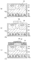
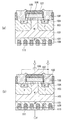
【解決手段】 半導体装置1aはMOSFETである。N+バルク層101において、主面101b側の表面領域には、高濃度のP型不純物を含むSiCを主組成としたP型領域109が形成されている。N+バルク層101の主面101b上には、N+バルク層101とオーミック接触を形成するドレイン電極膜109が形成されている。順方向サージが印加されても、N−ドリフト層102が伝導度変調され、オン抵抗が低下し、発熱量が低下するので、順方向サージに対する耐性を向上することができる。
【選択図】 図1
Description
Claims (2)
- 対向する第1および第2の主面を備え、第1導電型のSiCを含む第1の半導体層と、
前記第1の主面上に形成された、前記第1の半導体層よりも不純物濃度の低い第1導電型のSiCを含む第2の半導体層と、
前記第2の半導体層の表面領域に形成された、第2導電型のSiCを含む第1の導電領域と、
前記第1の導電領域の表面領域に形成された、前記第2の半導体層よりも不純物濃度の高い第1導電型のSiCを含む第2の導電領域と、
絶縁膜を隔てて前記第1の導電領域および前記第2の導電領域の一部と隣接するゲート電極膜と、
前記第2の導電領域上に形成された第1の電極膜と、
前記第1の半導体層において、前記第2の主面側の表面領域に形成された、第2導電型のSiCを含む第3の導電領域と、
前記第1の半導体層上および前記第3の導電領域上に形成された第2の電極膜と、
を有することを特徴とするSiC半導体装置。 - 対向する第1および第2の主面を備え、第1導電型のSiCを含む第1の半導体層と、
前記第1の主面上に形成された、前記第1の半導体層よりも不純物濃度の低い第1導電型のSiCを含む第2の半導体層と、
前記第2の半導体層の表面領域に形成された、第2導電型のSiCを含む第1の導電領域と、
前記第1の導電領域の表面領域に形成された、前記第2の半導体層よりも不純物濃度の高い第1導電型のSiCを含む第2の導電領域と、
絶縁膜を隔てて前記第1の導電領域および前記第2の導電領域の一部と隣接するゲート電極膜と、
前記第2の導電領域上に形成された第1の電極膜と、
前記第1の半導体層において、前記第2の主面側の表面領域に形成された、第2導電型のSiCを含む第3の導電領域と、
前記第1の半導体層上に形成された第2の電極膜と、
前記第3の導電領域上に形成され、前記第3の導電領域とオーミック接触を形成する第3の電極膜と、
を有することを特徴とするSiC半導体装置。
Priority Applications (1)
| Application Number | Priority Date | Filing Date | Title |
|---|---|---|---|
| JP2005151373A JP2006332199A (ja) | 2005-05-24 | 2005-05-24 | SiC半導体装置 |
Applications Claiming Priority (1)
| Application Number | Priority Date | Filing Date | Title |
|---|---|---|---|
| JP2005151373A JP2006332199A (ja) | 2005-05-24 | 2005-05-24 | SiC半導体装置 |
Publications (1)
| Publication Number | Publication Date |
|---|---|
| JP2006332199A true JP2006332199A (ja) | 2006-12-07 |
Family
ID=37553602
Family Applications (1)
| Application Number | Title | Priority Date | Filing Date |
|---|---|---|---|
| JP2005151373A Pending JP2006332199A (ja) | 2005-05-24 | 2005-05-24 | SiC半導体装置 |
Country Status (1)
| Country | Link |
|---|---|
| JP (1) | JP2006332199A (ja) |
Cited By (9)
| Publication number | Priority date | Publication date | Assignee | Title |
|---|---|---|---|---|
| JP2012156207A (ja) * | 2011-01-24 | 2012-08-16 | Mitsubishi Electric Corp | 半導体装置と半導体装置の製造方法 |
| JP2013232556A (ja) * | 2012-04-27 | 2013-11-14 | National Institute Of Advanced Industrial & Technology | 炭化珪素半導体素子の製造方法 |
| WO2013190907A1 (ja) * | 2012-06-21 | 2013-12-27 | 住友電気工業株式会社 | 炭化珪素半導体装置 |
| WO2014128839A1 (ja) * | 2013-02-20 | 2014-08-28 | 株式会社 日立製作所 | 半導体装置およびそれを用いた電力変換装置 |
| CN110767753A (zh) * | 2019-11-13 | 2020-02-07 | 电子科技大学 | 一种SiC功率器件 |
| CN111524970A (zh) * | 2020-01-09 | 2020-08-11 | 杭州电子科技大学 | 一种4H-SiC沟槽绝缘栅双极型晶体管 |
| JP2021019044A (ja) * | 2019-07-18 | 2021-02-15 | 株式会社デンソー | スイッチング素子 |
| CN112447525A (zh) * | 2020-11-30 | 2021-03-05 | 北京时代民芯科技有限公司 | 一种改善槽栅vdmos器件寄生体二极管反向恢复特性的方法 |
| CN112687743A (zh) * | 2020-12-29 | 2021-04-20 | 电子科技大学 | 沟槽型碳化硅逆阻mosfet器件及其制备方法 |
Citations (10)
| Publication number | Priority date | Publication date | Assignee | Title |
|---|---|---|---|---|
| JPS60170263A (ja) * | 1984-02-15 | 1985-09-03 | Nec Corp | 縦型電界効果トランジスタ |
| JPS6180857A (ja) * | 1984-09-28 | 1986-04-24 | Hitachi Ltd | 半導体スイツチング装置 |
| JPS61121758A (ja) * | 1984-11-13 | 1986-06-09 | デイジタル イクイプメント コーポレーシヨン | ブラシレスの直流モータ |
| JPS6248073A (ja) * | 1985-08-27 | 1987-03-02 | Mitsubishi Electric Corp | 半導体装置 |
| JPS6489564A (en) * | 1987-09-30 | 1989-04-04 | Nec Corp | Semiconductor device |
| JPH0414263A (ja) * | 1990-05-07 | 1992-01-20 | Fuji Electric Co Ltd | 絶縁ゲート型バイポーラトランジスタ |
| JPH098301A (ja) * | 1995-04-20 | 1997-01-10 | Toshiba Corp | 電力用半導体装置 |
| JP2000012846A (ja) * | 1998-06-22 | 2000-01-14 | Denso Corp | 炭化珪素半導体装置及びその製造方法 |
| JP2001313393A (ja) * | 2000-04-28 | 2001-11-09 | Toshiba Corp | 電力用半導体装置及びその駆動方法 |
| JP2004146679A (ja) * | 2002-10-25 | 2004-05-20 | Toyota Central Res & Dev Lab Inc | バイポーラ型半導体装置とその製造方法 |
-
2005
- 2005-05-24 JP JP2005151373A patent/JP2006332199A/ja active Pending
Patent Citations (10)
| Publication number | Priority date | Publication date | Assignee | Title |
|---|---|---|---|---|
| JPS60170263A (ja) * | 1984-02-15 | 1985-09-03 | Nec Corp | 縦型電界効果トランジスタ |
| JPS6180857A (ja) * | 1984-09-28 | 1986-04-24 | Hitachi Ltd | 半導体スイツチング装置 |
| JPS61121758A (ja) * | 1984-11-13 | 1986-06-09 | デイジタル イクイプメント コーポレーシヨン | ブラシレスの直流モータ |
| JPS6248073A (ja) * | 1985-08-27 | 1987-03-02 | Mitsubishi Electric Corp | 半導体装置 |
| JPS6489564A (en) * | 1987-09-30 | 1989-04-04 | Nec Corp | Semiconductor device |
| JPH0414263A (ja) * | 1990-05-07 | 1992-01-20 | Fuji Electric Co Ltd | 絶縁ゲート型バイポーラトランジスタ |
| JPH098301A (ja) * | 1995-04-20 | 1997-01-10 | Toshiba Corp | 電力用半導体装置 |
| JP2000012846A (ja) * | 1998-06-22 | 2000-01-14 | Denso Corp | 炭化珪素半導体装置及びその製造方法 |
| JP2001313393A (ja) * | 2000-04-28 | 2001-11-09 | Toshiba Corp | 電力用半導体装置及びその駆動方法 |
| JP2004146679A (ja) * | 2002-10-25 | 2004-05-20 | Toyota Central Res & Dev Lab Inc | バイポーラ型半導体装置とその製造方法 |
Cited By (11)
| Publication number | Priority date | Publication date | Assignee | Title |
|---|---|---|---|---|
| JP2012156207A (ja) * | 2011-01-24 | 2012-08-16 | Mitsubishi Electric Corp | 半導体装置と半導体装置の製造方法 |
| JP2013232556A (ja) * | 2012-04-27 | 2013-11-14 | National Institute Of Advanced Industrial & Technology | 炭化珪素半導体素子の製造方法 |
| WO2013190907A1 (ja) * | 2012-06-21 | 2013-12-27 | 住友電気工業株式会社 | 炭化珪素半導体装置 |
| US8729567B2 (en) | 2012-06-21 | 2014-05-20 | Sumitomo Electric Industries, Ltd. | Silicon carbide semiconductor device |
| WO2014128839A1 (ja) * | 2013-02-20 | 2014-08-28 | 株式会社 日立製作所 | 半導体装置およびそれを用いた電力変換装置 |
| JP2021019044A (ja) * | 2019-07-18 | 2021-02-15 | 株式会社デンソー | スイッチング素子 |
| CN110767753A (zh) * | 2019-11-13 | 2020-02-07 | 电子科技大学 | 一种SiC功率器件 |
| CN111524970A (zh) * | 2020-01-09 | 2020-08-11 | 杭州电子科技大学 | 一种4H-SiC沟槽绝缘栅双极型晶体管 |
| CN112447525A (zh) * | 2020-11-30 | 2021-03-05 | 北京时代民芯科技有限公司 | 一种改善槽栅vdmos器件寄生体二极管反向恢复特性的方法 |
| CN112447525B (zh) * | 2020-11-30 | 2024-11-29 | 北京时代民芯科技有限公司 | 一种改善槽栅vdmos器件寄生体二极管反向恢复特性的方法 |
| CN112687743A (zh) * | 2020-12-29 | 2021-04-20 | 电子科技大学 | 沟槽型碳化硅逆阻mosfet器件及其制备方法 |
Similar Documents
| Publication | Publication Date | Title |
|---|---|---|
| JP7806834B2 (ja) | 半導体装置の製造方法 | |
| JP5787853B2 (ja) | 電力用半導体装置 | |
| US7157785B2 (en) | Semiconductor device, the method of manufacturing the same, and two-way switching device using the semiconductor devices | |
| JP4900662B2 (ja) | ショットキーダイオードを内蔵した炭化ケイ素mos電界効果トランジスタおよびその製造方法 | |
| JP5565461B2 (ja) | 半導体装置 | |
| CN108574000B9 (zh) | 半导体装置和半导体装置的制造方法 | |
| JP5321377B2 (ja) | 電力用半導体装置 | |
| CN102694009A (zh) | 半导体器件及其制造方法 | |
| JP4456013B2 (ja) | 半導体装置 | |
| JP2018107168A (ja) | 半導体装置および半導体装置の製造方法 | |
| CN111149213A (zh) | 碳化硅半导体装置及其制造方法 | |
| JP2009027152A (ja) | 半導体装置及び半導体装置の製造方法 | |
| CN108886038B (zh) | 半导体装置 | |
| JPWO2018037701A1 (ja) | 半導体装置 | |
| JP4761942B2 (ja) | 半導体装置 | |
| JPH07115189A (ja) | 絶縁ゲート型バイポーラトランジスタ | |
| CN118712230A (zh) | 一种低接触电阻率和沟道迁移率的mos半导体结构 | |
| JP2023042402A (ja) | 半導体装置 | |
| JP6648852B1 (ja) | 炭化珪素半導体装置および炭化珪素半導体装置の製造方法 | |
| JP5366521B2 (ja) | 炭化珪素半導体装置及びその製造方法 | |
| JPH0621358A (ja) | 絶縁ゲート型バイポーラトランジスタ | |
| JP2006332199A (ja) | SiC半導体装置 | |
| US20240213357A1 (en) | Semiconductor device and method of manufacturing the same | |
| JP4761011B2 (ja) | サイリスタを有する半導体装置及びその製造方法 | |
| JP6771433B2 (ja) | 半導体装置 |
Legal Events
| Date | Code | Title | Description |
|---|---|---|---|
| A621 | Written request for application examination |
Free format text: JAPANESE INTERMEDIATE CODE: A621 Effective date: 20070523 |
|
| A977 | Report on retrieval |
Free format text: JAPANESE INTERMEDIATE CODE: A971007 Effective date: 20110304 |
|
| A131 | Notification of reasons for refusal |
Free format text: JAPANESE INTERMEDIATE CODE: A131 Effective date: 20110412 |
|
| A521 | Request for written amendment filed |
Free format text: JAPANESE INTERMEDIATE CODE: A523 Effective date: 20110606 |
|
| A131 | Notification of reasons for refusal |
Free format text: JAPANESE INTERMEDIATE CODE: A131 Effective date: 20110705 |
|
| A02 | Decision of refusal |
Free format text: JAPANESE INTERMEDIATE CODE: A02 Effective date: 20111101 |