JP2006509232A - 有機ledディスプレイ装置及びそのような装置を駆動するための方法 - Google Patents
有機ledディスプレイ装置及びそのような装置を駆動するための方法 Download PDFInfo
- Publication number
- JP2006509232A JP2006509232A JP2004556644A JP2004556644A JP2006509232A JP 2006509232 A JP2006509232 A JP 2006509232A JP 2004556644 A JP2004556644 A JP 2004556644A JP 2004556644 A JP2004556644 A JP 2004556644A JP 2006509232 A JP2006509232 A JP 2006509232A
- Authority
- JP
- Japan
- Prior art keywords
- light emitting
- duty cycle
- voltage
- display device
- emitting element
- Prior art date
- Legal status (The legal status is an assumption and is not a legal conclusion. Google has not performed a legal analysis and makes no representation as to the accuracy of the status listed.)
- Pending
Links
- 238000000034 method Methods 0.000 title claims abstract description 23
- 239000012044 organic layer Substances 0.000 claims abstract description 9
- 239000011159 matrix material Substances 0.000 claims description 15
- 238000012544 monitoring process Methods 0.000 claims description 4
- RICKKZXCGCSLIU-UHFFFAOYSA-N 2-[2-[carboxymethyl-[[3-hydroxy-5-(hydroxymethyl)-2-methylpyridin-4-yl]methyl]amino]ethyl-[[3-hydroxy-5-(hydroxymethyl)-2-methylpyridin-4-yl]methyl]amino]acetic acid Chemical compound CC1=NC=C(CO)C(CN(CCN(CC(O)=O)CC=2C(=C(C)N=CC=2CO)O)CC(O)=O)=C1O RICKKZXCGCSLIU-UHFFFAOYSA-N 0.000 description 12
- 239000010410 layer Substances 0.000 description 12
- 229920000642 polymer Polymers 0.000 description 4
- 239000000470 constituent Substances 0.000 description 3
- 230000007423 decrease Effects 0.000 description 3
- 238000010586 diagram Methods 0.000 description 3
- 239000002699 waste material Substances 0.000 description 3
- 230000015572 biosynthetic process Effects 0.000 description 2
- 230000000694 effects Effects 0.000 description 2
- 230000002085 persistent effect Effects 0.000 description 2
- 238000009835 boiling Methods 0.000 description 1
- 238000000354 decomposition reaction Methods 0.000 description 1
- 230000007547 defect Effects 0.000 description 1
- 230000005684 electric field Effects 0.000 description 1
- 239000000463 material Substances 0.000 description 1
- 238000005259 measurement Methods 0.000 description 1
- 238000002844 melting Methods 0.000 description 1
- 230000008018 melting Effects 0.000 description 1
- 239000002052 molecular layer Substances 0.000 description 1
- 239000000615 nonconductor Substances 0.000 description 1
- 238000011017 operating method Methods 0.000 description 1
- 229920000620 organic polymer Polymers 0.000 description 1
- 239000002245 particle Substances 0.000 description 1
- 229910021420 polycrystalline silicon Inorganic materials 0.000 description 1
- 229920005591 polysilicon Polymers 0.000 description 1
- 238000011084 recovery Methods 0.000 description 1
- 238000011160 research Methods 0.000 description 1
Images




Classifications
-
- G—PHYSICS
- G09—EDUCATION; CRYPTOGRAPHY; DISPLAY; ADVERTISING; SEALS
- G09G—ARRANGEMENTS OR CIRCUITS FOR CONTROL OF INDICATING DEVICES USING STATIC MEANS TO PRESENT VARIABLE INFORMATION
- G09G3/00—Control arrangements or circuits, of interest only in connection with visual indicators other than cathode-ray tubes
- G09G3/20—Control arrangements or circuits, of interest only in connection with visual indicators other than cathode-ray tubes for presentation of an assembly of a number of characters, e.g. a page, by composing the assembly by combination of individual elements arranged in a matrix no fixed position being assigned to or needed to be assigned to the individual characters or partial characters
- G09G3/22—Control arrangements or circuits, of interest only in connection with visual indicators other than cathode-ray tubes for presentation of an assembly of a number of characters, e.g. a page, by composing the assembly by combination of individual elements arranged in a matrix no fixed position being assigned to or needed to be assigned to the individual characters or partial characters using controlled light sources
- G09G3/30—Control arrangements or circuits, of interest only in connection with visual indicators other than cathode-ray tubes for presentation of an assembly of a number of characters, e.g. a page, by composing the assembly by combination of individual elements arranged in a matrix no fixed position being assigned to or needed to be assigned to the individual characters or partial characters using controlled light sources using electroluminescent panels
-
- G—PHYSICS
- G09—EDUCATION; CRYPTOGRAPHY; DISPLAY; ADVERTISING; SEALS
- G09G—ARRANGEMENTS OR CIRCUITS FOR CONTROL OF INDICATING DEVICES USING STATIC MEANS TO PRESENT VARIABLE INFORMATION
- G09G3/00—Control arrangements or circuits, of interest only in connection with visual indicators other than cathode-ray tubes
- G09G3/20—Control arrangements or circuits, of interest only in connection with visual indicators other than cathode-ray tubes for presentation of an assembly of a number of characters, e.g. a page, by composing the assembly by combination of individual elements arranged in a matrix no fixed position being assigned to or needed to be assigned to the individual characters or partial characters
- G09G3/22—Control arrangements or circuits, of interest only in connection with visual indicators other than cathode-ray tubes for presentation of an assembly of a number of characters, e.g. a page, by composing the assembly by combination of individual elements arranged in a matrix no fixed position being assigned to or needed to be assigned to the individual characters or partial characters using controlled light sources
- G09G3/30—Control arrangements or circuits, of interest only in connection with visual indicators other than cathode-ray tubes for presentation of an assembly of a number of characters, e.g. a page, by composing the assembly by combination of individual elements arranged in a matrix no fixed position being assigned to or needed to be assigned to the individual characters or partial characters using controlled light sources using electroluminescent panels
- G09G3/32—Control arrangements or circuits, of interest only in connection with visual indicators other than cathode-ray tubes for presentation of an assembly of a number of characters, e.g. a page, by composing the assembly by combination of individual elements arranged in a matrix no fixed position being assigned to or needed to be assigned to the individual characters or partial characters using controlled light sources using electroluminescent panels semiconductive, e.g. using light-emitting diodes [LED]
- G09G3/3208—Control arrangements or circuits, of interest only in connection with visual indicators other than cathode-ray tubes for presentation of an assembly of a number of characters, e.g. a page, by composing the assembly by combination of individual elements arranged in a matrix no fixed position being assigned to or needed to be assigned to the individual characters or partial characters using controlled light sources using electroluminescent panels semiconductive, e.g. using light-emitting diodes [LED] organic, e.g. using organic light-emitting diodes [OLED]
- G09G3/3216—Control arrangements or circuits, of interest only in connection with visual indicators other than cathode-ray tubes for presentation of an assembly of a number of characters, e.g. a page, by composing the assembly by combination of individual elements arranged in a matrix no fixed position being assigned to or needed to be assigned to the individual characters or partial characters using controlled light sources using electroluminescent panels semiconductive, e.g. using light-emitting diodes [LED] organic, e.g. using organic light-emitting diodes [OLED] using a passive matrix
-
- G—PHYSICS
- G09—EDUCATION; CRYPTOGRAPHY; DISPLAY; ADVERTISING; SEALS
- G09G—ARRANGEMENTS OR CIRCUITS FOR CONTROL OF INDICATING DEVICES USING STATIC MEANS TO PRESENT VARIABLE INFORMATION
- G09G3/00—Control arrangements or circuits, of interest only in connection with visual indicators other than cathode-ray tubes
- G09G3/20—Control arrangements or circuits, of interest only in connection with visual indicators other than cathode-ray tubes for presentation of an assembly of a number of characters, e.g. a page, by composing the assembly by combination of individual elements arranged in a matrix no fixed position being assigned to or needed to be assigned to the individual characters or partial characters
- G09G3/22—Control arrangements or circuits, of interest only in connection with visual indicators other than cathode-ray tubes for presentation of an assembly of a number of characters, e.g. a page, by composing the assembly by combination of individual elements arranged in a matrix no fixed position being assigned to or needed to be assigned to the individual characters or partial characters using controlled light sources
- G09G3/30—Control arrangements or circuits, of interest only in connection with visual indicators other than cathode-ray tubes for presentation of an assembly of a number of characters, e.g. a page, by composing the assembly by combination of individual elements arranged in a matrix no fixed position being assigned to or needed to be assigned to the individual characters or partial characters using controlled light sources using electroluminescent panels
- G09G3/32—Control arrangements or circuits, of interest only in connection with visual indicators other than cathode-ray tubes for presentation of an assembly of a number of characters, e.g. a page, by composing the assembly by combination of individual elements arranged in a matrix no fixed position being assigned to or needed to be assigned to the individual characters or partial characters using controlled light sources using electroluminescent panels semiconductive, e.g. using light-emitting diodes [LED]
- G09G3/3208—Control arrangements or circuits, of interest only in connection with visual indicators other than cathode-ray tubes for presentation of an assembly of a number of characters, e.g. a page, by composing the assembly by combination of individual elements arranged in a matrix no fixed position being assigned to or needed to be assigned to the individual characters or partial characters using controlled light sources using electroluminescent panels semiconductive, e.g. using light-emitting diodes [LED] organic, e.g. using organic light-emitting diodes [OLED]
- G09G3/3225—Control arrangements or circuits, of interest only in connection with visual indicators other than cathode-ray tubes for presentation of an assembly of a number of characters, e.g. a page, by composing the assembly by combination of individual elements arranged in a matrix no fixed position being assigned to or needed to be assigned to the individual characters or partial characters using controlled light sources using electroluminescent panels semiconductive, e.g. using light-emitting diodes [LED] organic, e.g. using organic light-emitting diodes [OLED] using an active matrix
- G09G3/3233—Control arrangements or circuits, of interest only in connection with visual indicators other than cathode-ray tubes for presentation of an assembly of a number of characters, e.g. a page, by composing the assembly by combination of individual elements arranged in a matrix no fixed position being assigned to or needed to be assigned to the individual characters or partial characters using controlled light sources using electroluminescent panels semiconductive, e.g. using light-emitting diodes [LED] organic, e.g. using organic light-emitting diodes [OLED] using an active matrix with pixel circuitry controlling the current through the light-emitting element
-
- G—PHYSICS
- G09—EDUCATION; CRYPTOGRAPHY; DISPLAY; ADVERTISING; SEALS
- G09G—ARRANGEMENTS OR CIRCUITS FOR CONTROL OF INDICATING DEVICES USING STATIC MEANS TO PRESENT VARIABLE INFORMATION
- G09G2300/00—Aspects of the constitution of display devices
- G09G2300/08—Active matrix structure, i.e. with use of active elements, inclusive of non-linear two terminal elements, in the pixels together with light emitting or modulating elements
- G09G2300/0809—Several active elements per pixel in active matrix panels
- G09G2300/0842—Several active elements per pixel in active matrix panels forming a memory circuit, e.g. a dynamic memory with one capacitor
-
- G—PHYSICS
- G09—EDUCATION; CRYPTOGRAPHY; DISPLAY; ADVERTISING; SEALS
- G09G—ARRANGEMENTS OR CIRCUITS FOR CONTROL OF INDICATING DEVICES USING STATIC MEANS TO PRESENT VARIABLE INFORMATION
- G09G2320/00—Control of display operating conditions
- G09G2320/04—Maintaining the quality of display appearance
- G09G2320/043—Preventing or counteracting the effects of ageing
-
- G—PHYSICS
- G09—EDUCATION; CRYPTOGRAPHY; DISPLAY; ADVERTISING; SEALS
- G09G—ARRANGEMENTS OR CIRCUITS FOR CONTROL OF INDICATING DEVICES USING STATIC MEANS TO PRESENT VARIABLE INFORMATION
- G09G3/00—Control arrangements or circuits, of interest only in connection with visual indicators other than cathode-ray tubes
- G09G3/20—Control arrangements or circuits, of interest only in connection with visual indicators other than cathode-ray tubes for presentation of an assembly of a number of characters, e.g. a page, by composing the assembly by combination of individual elements arranged in a matrix no fixed position being assigned to or needed to be assigned to the individual characters or partial characters
- G09G3/2007—Display of intermediate tones
- G09G3/2014—Display of intermediate tones by modulation of the duration of a single pulse during which the logic level remains constant
-
- G—PHYSICS
- G09—EDUCATION; CRYPTOGRAPHY; DISPLAY; ADVERTISING; SEALS
- G09G—ARRANGEMENTS OR CIRCUITS FOR CONTROL OF INDICATING DEVICES USING STATIC MEANS TO PRESENT VARIABLE INFORMATION
- G09G3/00—Control arrangements or circuits, of interest only in connection with visual indicators other than cathode-ray tubes
- G09G3/20—Control arrangements or circuits, of interest only in connection with visual indicators other than cathode-ray tubes for presentation of an assembly of a number of characters, e.g. a page, by composing the assembly by combination of individual elements arranged in a matrix no fixed position being assigned to or needed to be assigned to the individual characters or partial characters
- G09G3/2007—Display of intermediate tones
- G09G3/2077—Display of intermediate tones by a combination of two or more gradation control methods
-
- G—PHYSICS
- G09—EDUCATION; CRYPTOGRAPHY; DISPLAY; ADVERTISING; SEALS
- G09G—ARRANGEMENTS OR CIRCUITS FOR CONTROL OF INDICATING DEVICES USING STATIC MEANS TO PRESENT VARIABLE INFORMATION
- G09G3/00—Control arrangements or circuits, of interest only in connection with visual indicators other than cathode-ray tubes
- G09G3/20—Control arrangements or circuits, of interest only in connection with visual indicators other than cathode-ray tubes for presentation of an assembly of a number of characters, e.g. a page, by composing the assembly by combination of individual elements arranged in a matrix no fixed position being assigned to or needed to be assigned to the individual characters or partial characters
- G09G3/22—Control arrangements or circuits, of interest only in connection with visual indicators other than cathode-ray tubes for presentation of an assembly of a number of characters, e.g. a page, by composing the assembly by combination of individual elements arranged in a matrix no fixed position being assigned to or needed to be assigned to the individual characters or partial characters using controlled light sources
- G09G3/30—Control arrangements or circuits, of interest only in connection with visual indicators other than cathode-ray tubes for presentation of an assembly of a number of characters, e.g. a page, by composing the assembly by combination of individual elements arranged in a matrix no fixed position being assigned to or needed to be assigned to the individual characters or partial characters using controlled light sources using electroluminescent panels
- G09G3/32—Control arrangements or circuits, of interest only in connection with visual indicators other than cathode-ray tubes for presentation of an assembly of a number of characters, e.g. a page, by composing the assembly by combination of individual elements arranged in a matrix no fixed position being assigned to or needed to be assigned to the individual characters or partial characters using controlled light sources using electroluminescent panels semiconductive, e.g. using light-emitting diodes [LED]
- G09G3/3208—Control arrangements or circuits, of interest only in connection with visual indicators other than cathode-ray tubes for presentation of an assembly of a number of characters, e.g. a page, by composing the assembly by combination of individual elements arranged in a matrix no fixed position being assigned to or needed to be assigned to the individual characters or partial characters using controlled light sources using electroluminescent panels semiconductive, e.g. using light-emitting diodes [LED] organic, e.g. using organic light-emitting diodes [OLED]
- G09G3/3275—Details of drivers for data electrodes
- G09G3/3291—Details of drivers for data electrodes in which the data driver supplies a variable data voltage for setting the current through, or the voltage across, the light-emitting elements
Landscapes
- Engineering & Computer Science (AREA)
- Physics & Mathematics (AREA)
- Computer Hardware Design (AREA)
- General Physics & Mathematics (AREA)
- Theoretical Computer Science (AREA)
- Control Of Indicators Other Than Cathode Ray Tubes (AREA)
- Electroluminescent Light Sources (AREA)
- Control Of El Displays (AREA)
Abstract
Description
Pshort=αAdev (2)
ここで、αは、短絡確立と装置面積との間の比例定数である。
I) 小さい電圧値に対しては、リーク電流の不安定性が小さいことが実験的に分かった
静電引力は、尚も小さ過ぎて、直接接触は引き起こされない。これは、構成層の弾性特性に直接関係している。更に、浪費されるエネルギー(〜Vappl/Rcbannelであって、ここで、Vapplは印加電圧であり、Rcbannelは局部リーク経路の抵抗である)は小さ過ぎて、損傷を引き起こすことはない。
II) この電圧区画において、“フュージンング”は強い電流不安定性をもたらす。その電圧によりもたらされる静電引力は、陽極に対して陰極を圧する。しかしながら、その結果もたらされる損傷は、新しい接触であって、それ故、損傷等をもたらし、短絡回路が拡大する。又、短絡回路確率は、典型的には、損傷領域(リークチャネル)の周囲の長さと共に増加し、この電圧区画において生じる損傷の増加はこの周囲の長さの増加をもたらすため、短絡確率も又、増加する。
III) 5乃至10Vの範囲内の電圧においては又、短絡回路確率の強い減少が観測された。特定の電圧(VFUSE)以上で、不安定性は消え、リーク電流は減少する。上記のような各層間の付着力の人為的な増加は、回復確率を支持する(損傷におけるRcbannelの増加)。この第3の区画は、LED駆動に対して好適な区画である。
IV) 特定の閾値以上の電圧(典型的には70nmの厚さの有機層地に対して〜10V)に対して、装置全ては、リーク電流が非常に大きい状態にある傾向にあることが、実験的に観測された。その結果、短絡回路になる。明らかに、局部温度(浪費電力、〜Vappl/Rchannelに直接関係する)は、電極の一が分解する位高い値に達し、又は各層間の付着力がある他の様式(例えば、ガス発生)で破壊される位高い値に達する。実験的に又、この効果は、電圧の関数として非常に突然発生することが理解された。その閾値(Vth)は、高分子の種類及び装置の構成の関数として変化することが理解された。
VFUSE<Vappl<Vth (3)
それにより、式(1)において述べた装置電流比に関する結論、即ち、低短絡回路確率を達成するために必要な
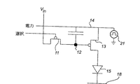
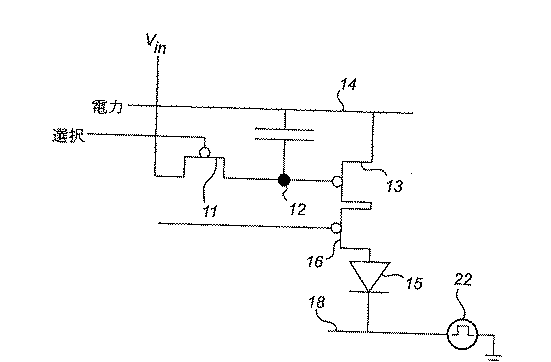
回路構成21を備えている。この“電力ラインデューティサイクル”は、電源が高電圧に設定されるときにのみ、画素が発光することができるため、PLED/OLED画素のデューティサイクルを順に規定する。この実施形態に従って、それ故、電力ラインが高電圧になるフレームの期間を調節することによりデューティサイクルを変更することができる。
Claims (21)
- 複数の発光素子を規定する有機層を挟む第1電極及び第2電極を有する有機LEDディスプレイ装置を駆動するための方法であって:
前記電極間の短絡回路のリスクが低減された特定の電圧範囲内の電圧を発光素子に印加する段階;並びに
所望の光強度が前記発光素子から発光されるように、前記発光素子のデューティサイクルを制御する段階;
を有することを特徴とする方法。 - 請求項1に記載の方法であって、前記発光素子の前記デューティサイクルは、特定の下限より小さい印加電圧を必要としないで、所望の光強度を発光するように減少される、ことを特徴とする方法。
- 請求項1に記載の方法であって、前記発光素子のデフォルトデューティサイクルは100%より小さく、前記デューティサイクルは、特定の上限より大きい印加電圧を必要としないで、所望の光強度を発光するように増加される、ことを特徴とする方法。
- 請求項2又は3に記載の方法であって:
前記発光素子において一定の駆動電流を維持する必要がある時間に亘って想定される電圧変化を決定する段階;及び
それに応じて、前記発光素子のデューティサイクルを調節する段階;
を更に有する、ことを特徴とする方法。 - 請求項2又は3に記載の方法であって:
前記ディスプレイにおける平均画素電圧をモニタリングする段階;及び
この平均電圧に従って、各々の発光素子のデューティサイクルを調節する段階;
を更に有する、ことを特徴とする方法。 - 請求項2又は3に記載の方法であって:
発光素子の電圧をモニタリングする段階;及び
この平均電圧に従って、前記発光素子のデューティサイクルを調節する段階;
を更に有する、ことを特徴とする方法。 - 請求項1乃至6のいずれ一項に記載の方法であって、前記デューティサイクルは各々のフレームにおいて制御される、ことを特徴とする方法。
- 請求項1乃至6のいずれ一項に記載の方法であって、前記デューティサイクルは複数のフレームにおいて制御される、ことを特徴とする方法。
- 請求項1乃至8のいずれ一項に記載の方法であって、前記ディスプレイ装置はアクティブマトリクス型である、ことを特徴とする方法。
- 請求項9に記載の方法であって、前記デューティサイクルは各々の発光素子に対して個別に制御される、ことを特徴とする方法。
- 請求項9に記載の方法であって、前記デューティサイクルは複数の発光素子に対して一緒に制御される、ことを特徴とする方法。
- 請求項8に記載の方法であって、前記ディスプレイ装置はパッシブマトリクス型である、ことを特徴とする方法。
- 請求項1乃至12にいずれ一項に従って駆動されるように備えられていることを特徴とする有機ディスプレイ装置。
- 複数の発光素子を規定する有機層を挟む第1電極及び第2電極を有する有機ディスプレイ装置であって:
発光素子に電圧を印加するための手段であって、前記電圧は、前記電極間における短絡回路のリスクが低減される特定の電圧範囲にある、手段;並びに
所望の光強度が前記発光素子から発光されるように、前記発光素子のデューティサイクルを制御するための手段;
を有することを特徴とする有機ディスプレイ装置。 - 請求項14に記載の有機ディスプレイ装置であって、前記制御手段は、特定の下限より小さい印加電圧を必要としないで、所望の光強度を発光するようにデューティサイクルを減少させるように備えられている、ことを特徴とする有機ディスプレイ装置。
- 請求項14に記載の有機ディスプレイ装置であって、前記制御手段は、100%より小さい、前記発光素子のデフォルトデューティサイクルを維持するように、及び、特定の上限より大きい印加電圧を必要としないで、所望の光強度を発光するように前記デューティサイクルを増加させるように備えられている、ことを特徴とする有機ディスプレイ装置。
- 請求項14乃至16のいずれ一項に記載の有機ディスプレイ装置であって、前記制御手段は、発光素子と電圧印加手段との間に接続されたトランジスタと、該トランジスタのゲートに接続されたデューティサイクル制御器とを有する、ことを特徴とする有機ディスプレイ装置。
- 請求項14乃至16のいずれ一項に記載の有機ディスプレイ装置であって、前記制御手段は、前記電圧印加手段に接続されたデューティサイクル制御器を有する、ことを特徴とする有機ディスプレイ装置。
- 請求項14乃至16のいずれ一項に記載の有機ディスプレイ装置であって、前記制御手段は、前記電圧印加手段に関連して前記発光素子の他の側に接続されたデューティサイクル制御器を有する、ことを特徴とする有機ディスプレイ装置。
- 請求項14乃至19のいずれ一項に記載の有機ディスプレイ装置であって、前記電圧印加手段は、電力ラインと、該電力ラインと前記発光素子との間に接続された駆動トランジスタとを有する、ことを特徴とする有機ディスプレイ装置。
- 請求項14乃至20のいずれ一項に記載の有機ディスプレイ装置であって、前記制御手段は、複数の発光素子に対するデューティサイクルを一緒に制御するように備えられている、ことを特徴とする有機ディスプレイ装置。
Applications Claiming Priority (2)
| Application Number | Priority Date | Filing Date | Title |
|---|---|---|---|
| EP02102680 | 2002-12-04 | ||
| PCT/IB2003/005432 WO2004051616A2 (en) | 2002-12-04 | 2003-11-25 | An organic led display device and a method for driving such a device |
Publications (1)
| Publication Number | Publication Date |
|---|---|
| JP2006509232A true JP2006509232A (ja) | 2006-03-16 |
Family
ID=32405774
Family Applications (1)
| Application Number | Title | Priority Date | Filing Date |
|---|---|---|---|
| JP2004556644A Pending JP2006509232A (ja) | 2002-12-04 | 2003-11-25 | 有機ledディスプレイ装置及びそのような装置を駆動するための方法 |
Country Status (9)
| Country | Link |
|---|---|
| US (1) | US20060092146A1 (ja) |
| EP (1) | EP1570458B1 (ja) |
| JP (1) | JP2006509232A (ja) |
| KR (1) | KR101021083B1 (ja) |
| CN (1) | CN100446068C (ja) |
| AT (1) | ATE541284T1 (ja) |
| AU (1) | AU2003282285A1 (ja) |
| ES (1) | ES2380661T3 (ja) |
| WO (1) | WO2004051616A2 (ja) |
Families Citing this family (15)
| Publication number | Priority date | Publication date | Assignee | Title |
|---|---|---|---|---|
| KR100707640B1 (ko) | 2005-04-28 | 2007-04-12 | 삼성에스디아이 주식회사 | 발광 표시장치 및 그 구동 방법 |
| US20070024537A1 (en) * | 2005-08-01 | 2007-02-01 | Osram Opto Semiconductors Gmbh | Drive scheme for improved device lifetime |
| JP5050462B2 (ja) * | 2006-09-15 | 2012-10-17 | ソニー株式会社 | 焼き付き抑制装置、自発光表示装置、画像処理装置、電子機器、焼き付き抑制方法及びコンピュータプログラム |
| US7888506B2 (en) * | 2007-01-26 | 2011-02-15 | Duquesne University Of The Holy Spirit | Composition, synthesis, and use of a new class of fluorophores |
| KR20120028426A (ko) * | 2010-09-14 | 2012-03-23 | 삼성모바일디스플레이주식회사 | 유기 발광 표시 장치 및 그것의 구동 방법 |
| FR2966276B1 (fr) | 2010-10-15 | 2013-03-08 | Commissariat Energie Atomique | Ecran d'affichage a diodes electroluminescentes a matrice active pourvu de moyens d'attenuation |
| KR20140111502A (ko) * | 2013-03-11 | 2014-09-19 | 삼성디스플레이 주식회사 | 표시장치 및 그 구동 방법 |
| KR102431363B1 (ko) | 2015-06-30 | 2022-08-09 | 엘지디스플레이 주식회사 | 유기 발광 표시 장치 및 그 구동 방법 |
| CN108630151B (zh) * | 2018-05-17 | 2022-08-26 | 京东方科技集团股份有限公司 | 像素电路及其驱动方法、阵列基板及显示装置 |
| CN109860271B (zh) * | 2019-04-16 | 2021-03-02 | 京东方科技集团股份有限公司 | 显示面板及其读取电路、显示终端 |
| US11615740B1 (en) | 2019-12-13 | 2023-03-28 | Meta Platforms Technologies, Llc | Content-adaptive duty ratio control |
| US11567325B2 (en) | 2020-10-09 | 2023-01-31 | Meta Platforms Technologies, Llc | Artificial reality systems including digital and analog control of pixel intensity |
| US11922892B2 (en) | 2021-01-20 | 2024-03-05 | Meta Platforms Technologies, Llc | High-efficiency backlight driver |
| CN113053301B (zh) * | 2021-03-23 | 2022-08-19 | 京东方科技集团股份有限公司 | 像素驱动电路、像素驱动方法、显示面板及显示装置 |
| US12183280B2 (en) * | 2021-07-01 | 2024-12-31 | Universal Display Corporation | Means to reduce OLED transient response |
Citations (4)
| Publication number | Priority date | Publication date | Assignee | Title |
|---|---|---|---|---|
| JPH11233264A (ja) * | 1998-02-12 | 1999-08-27 | Casio Comput Co Ltd | 表示装置及びその駆動方法 |
| JP2001261677A (ja) * | 2000-03-14 | 2001-09-26 | Fuji Photo Film Co Ltd | 発光素子材料、それを使用した発光素子及び環状アジン化合物 |
| JP2001350442A (ja) * | 1999-10-04 | 2001-12-21 | Matsushita Electric Ind Co Ltd | 表示パネルの駆動方法、表示パネルの輝度補正装置及び駆動装置 |
| JP2002313567A (ja) * | 2001-04-18 | 2002-10-25 | Sony Corp | 有機電界発光素子及びその製造方法 |
Family Cites Families (23)
| Publication number | Priority date | Publication date | Assignee | Title |
|---|---|---|---|---|
| EP0923067B1 (en) * | 1997-03-12 | 2004-08-04 | Seiko Epson Corporation | Pixel circuit, display device and electronic equipment having current-driven light-emitting device |
| US6023259A (en) * | 1997-07-11 | 2000-02-08 | Fed Corporation | OLED active matrix using a single transistor current mode pixel design |
| US6023225A (en) * | 1997-07-17 | 2000-02-08 | Jeffrey V. Boley | Golf equipment inventory device |
| US6355393B1 (en) * | 1999-03-10 | 2002-03-12 | Fuji Photo Film Co., Ltd. | Image-forming method and organic light-emitting element for a light source for exposure used therein |
| JP4092857B2 (ja) * | 1999-06-17 | 2008-05-28 | ソニー株式会社 | 画像表示装置 |
| JP2001013903A (ja) * | 1999-06-28 | 2001-01-19 | Seiko Instruments Inc | 自発光表示素子駆動装置 |
| EP1079361A1 (en) * | 1999-08-20 | 2001-02-28 | Harness System Technologies Research, Ltd. | Driver for electroluminescent elements |
| KR100858065B1 (ko) * | 1999-09-22 | 2008-09-10 | 코닌클리케 필립스 일렉트로닉스 엔.브이. | 발광 디바이스, 및 이를 제조 및 시험하는 방법 |
| US7227519B1 (en) * | 1999-10-04 | 2007-06-05 | Matsushita Electric Industrial Co., Ltd. | Method of driving display panel, luminance correction device for display panel, and driving device for display panel |
| JP2001109432A (ja) * | 1999-10-06 | 2001-04-20 | Pioneer Electronic Corp | アクティブマトリックス型発光パネルの駆動装置 |
| US20020030647A1 (en) * | 2000-06-06 | 2002-03-14 | Michael Hack | Uniform active matrix oled displays |
| US6677709B1 (en) * | 2000-07-18 | 2004-01-13 | General Electric Company | Micro electromechanical system controlled organic led and pixel arrays and method of using and of manufacturing same |
| US6580657B2 (en) * | 2001-01-04 | 2003-06-17 | International Business Machines Corporation | Low-power organic light emitting diode pixel circuit |
| TWI248319B (en) * | 2001-02-08 | 2006-01-21 | Semiconductor Energy Lab | Light emitting device and electronic equipment using the same |
| CN1265339C (zh) * | 2001-03-21 | 2006-07-19 | 佳能株式会社 | 有源矩阵型发光元件的驱动电路 |
| US6734636B2 (en) * | 2001-06-22 | 2004-05-11 | International Business Machines Corporation | OLED current drive pixel circuit |
| US6664730B2 (en) * | 2001-07-09 | 2003-12-16 | Universal Display Corporation | Electrode structure of el device |
| US6984934B2 (en) * | 2001-07-10 | 2006-01-10 | The Trustees Of Princeton University | Micro-lens arrays for display intensity enhancement |
| DE60218488T2 (de) * | 2001-08-23 | 2007-10-31 | Koninklijke Philips Electronics N.V. | Verfahren und ansteuermittel zur farbkorrektur in einem organischen elektrolumineszenzbauelement |
| US6872974B2 (en) * | 2001-11-20 | 2005-03-29 | International Business Machines Corporation | Low threshold voltage instability amorphous silicon field effect transistor structure and biasing for active matrix organic light-emitting diodes |
| US7071932B2 (en) * | 2001-11-20 | 2006-07-04 | Toppoly Optoelectronics Corporation | Data voltage current drive amoled pixel circuit |
| US20030122748A1 (en) * | 2001-12-27 | 2003-07-03 | Kuan-Jui Ho | Method for driving a passive matrix OEL device |
| US6847340B2 (en) * | 2002-08-16 | 2005-01-25 | Windell Corporation | Active organic light emitting diode drive circuit |
-
2003
- 2003-11-25 JP JP2004556644A patent/JP2006509232A/ja active Pending
- 2003-11-25 US US10/536,845 patent/US20060092146A1/en not_active Abandoned
- 2003-11-25 AU AU2003282285A patent/AU2003282285A1/en not_active Abandoned
- 2003-11-25 CN CNB2003801051759A patent/CN100446068C/zh not_active Expired - Lifetime
- 2003-11-25 AT AT03773903T patent/ATE541284T1/de active
- 2003-11-25 EP EP03773903A patent/EP1570458B1/en not_active Expired - Lifetime
- 2003-11-25 ES ES03773903T patent/ES2380661T3/es not_active Expired - Lifetime
- 2003-11-25 KR KR1020057009867A patent/KR101021083B1/ko not_active Expired - Lifetime
- 2003-11-25 WO PCT/IB2003/005432 patent/WO2004051616A2/en not_active Ceased
Patent Citations (4)
| Publication number | Priority date | Publication date | Assignee | Title |
|---|---|---|---|---|
| JPH11233264A (ja) * | 1998-02-12 | 1999-08-27 | Casio Comput Co Ltd | 表示装置及びその駆動方法 |
| JP2001350442A (ja) * | 1999-10-04 | 2001-12-21 | Matsushita Electric Ind Co Ltd | 表示パネルの駆動方法、表示パネルの輝度補正装置及び駆動装置 |
| JP2001261677A (ja) * | 2000-03-14 | 2001-09-26 | Fuji Photo Film Co Ltd | 発光素子材料、それを使用した発光素子及び環状アジン化合物 |
| JP2002313567A (ja) * | 2001-04-18 | 2002-10-25 | Sony Corp | 有機電界発光素子及びその製造方法 |
Also Published As
| Publication number | Publication date |
|---|---|
| WO2004051616A2 (en) | 2004-06-17 |
| ES2380661T3 (es) | 2012-05-17 |
| AU2003282285A1 (en) | 2004-06-23 |
| EP1570458B1 (en) | 2012-01-11 |
| CN1720568A (zh) | 2006-01-11 |
| US20060092146A1 (en) | 2006-05-04 |
| KR101021083B1 (ko) | 2011-03-14 |
| EP1570458A2 (en) | 2005-09-07 |
| WO2004051616A3 (en) | 2004-08-26 |
| CN100446068C (zh) | 2008-12-24 |
| ATE541284T1 (de) | 2012-01-15 |
| KR20050087818A (ko) | 2005-08-31 |
Similar Documents
| Publication | Publication Date | Title |
|---|---|---|
| CN100452155C (zh) | 显示装置和显示方法 | |
| JP4836402B2 (ja) | 自発光型表示装置 | |
| CN100446068C (zh) | 有机led显示器件及其驱动方法 | |
| KR100526267B1 (ko) | 디스플레이 장치, oled 패널, 박막 트랜지스터의 제어장치, 박막 트랜지스터의 제어 방법 및 oled디스플레이의 제어 방법 | |
| JP3775628B2 (ja) | 電荷蓄積性発光素子の駆動装置及び駆動方法 | |
| CN100452137C (zh) | 用于oled无源矩阵显示器的驱动器 | |
| US10482813B2 (en) | Power off method of display device, and display device | |
| US9117406B2 (en) | Display apparatus and control method for display apparatus | |
| CN100468496C (zh) | 显示设备及其控制方法 | |
| CN1381032A (zh) | 有源矩阵电致发光显示设备 | |
| CN101884061A (zh) | 具有控制电路的led显示器 | |
| KR102784315B1 (ko) | 표시 장치 및 그 구동 방법 | |
| JP2006071686A (ja) | 発光表示パネルの駆動装置 | |
| KR20060033746A (ko) | 전자발광 디스플레이 디바이스 | |
| JP2005539253A (ja) | 可変デューティサイクルをもつアクティブマトリクス型ディスプレイ | |
| JP5470668B2 (ja) | アクティブマトリクス型表示装置 | |
| WO2010001576A1 (ja) | 表示装置および表示装置の制御方法 | |
| JP2005227310A (ja) | 発光素子の駆動方法、画素回路、および表示装置 | |
| JP2008225188A (ja) | 発光表示パネルの駆動方法および駆動装置 | |
| JP2000330517A (ja) | 表示装置及びその駆動方法 | |
| JP3953996B2 (ja) | 表示装置および表示パネルの駆動方法 | |
| JP2008191684A (ja) | アクティブマトリクス型表示装置 | |
| JP2006210213A (ja) | 自発光装置のエージング方法、製造方法及びエージング装置 | |
| JP2006195030A (ja) | 自発光装置のエージング方法、製造方法及びエージング装置 | |
| JP5533737B2 (ja) | 有機el駆動装置 |
Legal Events
| Date | Code | Title | Description |
|---|---|---|---|
| A621 | Written request for application examination |
Free format text: JAPANESE INTERMEDIATE CODE: A621 Effective date: 20061122 |
|
| A131 | Notification of reasons for refusal |
Free format text: JAPANESE INTERMEDIATE CODE: A131 Effective date: 20100525 |
|
| A521 | Request for written amendment filed |
Free format text: JAPANESE INTERMEDIATE CODE: A523 Effective date: 20100820 |
|
| A131 | Notification of reasons for refusal |
Free format text: JAPANESE INTERMEDIATE CODE: A131 Effective date: 20101109 |
|
| A521 | Request for written amendment filed |
Free format text: JAPANESE INTERMEDIATE CODE: A523 Effective date: 20110208 |
|
| A02 | Decision of refusal |
Free format text: JAPANESE INTERMEDIATE CODE: A02 Effective date: 20111004 |