JP2007102902A - Semiconductor memory device and inspection method thereof - Google Patents
Semiconductor memory device and inspection method thereof Download PDFInfo
- Publication number
- JP2007102902A JP2007102902A JP2005290283A JP2005290283A JP2007102902A JP 2007102902 A JP2007102902 A JP 2007102902A JP 2005290283 A JP2005290283 A JP 2005290283A JP 2005290283 A JP2005290283 A JP 2005290283A JP 2007102902 A JP2007102902 A JP 2007102902A
- Authority
- JP
- Japan
- Prior art keywords
- bit line
- precharge
- memory device
- semiconductor memory
- circuit
- Prior art date
- Legal status (The legal status is an assumption and is not a legal conclusion. Google has not performed a legal analysis and makes no representation as to the accuracy of the status listed.)
- Pending
Links
Images


Landscapes
- For Increasing The Reliability Of Semiconductor Memories (AREA)
- Tests Of Electronic Circuits (AREA)
- Static Random-Access Memory (AREA)
Abstract
【課題】 SRAMの検査において、SNM値不足による信頼性不良を初期検査でスクリーングすることを可能とする。
【解決手段】 SRAMのビット線対の各ビット線のそれぞれに、通常動作用プリチャージ回路と検査用プリチャージ回路の各一端が並列接続される。通常動作用プリチャージ回路と検査用プリチャージ回路とは、同一の電源電圧に接続される。ビット線対の各ビット線のそれぞれに接続された通常動作用プリチャージ回路は同一の第1の活性化信号で、ビット線対の一方のビット線に接続された検査用プリチャージ回路は第2の活性化信号で、ビット線対の他方のビット線に接続された検査用プリチャージ回路は第3の活性化信号でそれぞれ活性化される。検査時において、読出し動作前に第2または第3の活性化信号の活性化によって、ビット線対の一方のビット線と他方のビット線とを互いに異なるプリチャージ電位までプリチャージする。
【選択図】 図1(a)PROBLEM TO BE SOLVED: To screen a reliability failure due to a shortage of an SNM value in an initial inspection in an SRAM inspection.
Each end of a normal operation precharge circuit and a test precharge circuit is connected in parallel to each bit line of an SRAM bit line pair. The normal operation precharge circuit and the inspection precharge circuit are connected to the same power supply voltage. The normal operation precharge circuit connected to each bit line of the bit line pair is the same first activation signal, and the test precharge circuit connected to one bit line of the bit line pair is the second. The test precharge circuit connected to the other bit line of the bit line pair is activated by the third activation signal. At the time of inspection, before the read operation, the activation of the second or third activation signal precharges one bit line and the other bit line of the bit line pair to different precharge potentials.
[Selection] Figure 1 (a)
Description
本発明は、半導体記憶装置、及びその検査方法に関し、特にスタティックランダムアクセスメモリの回路方式、及びその信頼性不良をスクリーニングする方法に関するものである。 The present invention relates to a semiconductor memory device and an inspection method thereof, and more particularly to a circuit system of a static random access memory and a method of screening for a reliability failure thereof.
近年、半導体集積回路装置の高機能化に伴い、スタティックランダムアクセスメモリ(以下SRAMと称す)が、その高速性と、制御とシステム組み込みの簡易性から半導体集積回路装置上に多く搭載されている。 2. Description of the Related Art In recent years, with increasing functionality of semiconductor integrated circuit devices, many static random access memories (hereinafter referred to as SRAM) are mounted on semiconductor integrated circuit devices because of their high speed and ease of control and system integration.
ところが、SRAMのメモリセルを構成するトランジスタが、製造工程で発生する微細な異物により汚染されると、その異物を含んだ半導体素子は所望の動作をせず、したがって所定の特性を得られずに不良となる。このような特性不良を発生した半導体素子を市場に出さないために、通常、出荷時に検査を行って不良素子をスクリーニングする。 However, when a transistor constituting an SRAM memory cell is contaminated by minute foreign matter generated in the manufacturing process, the semiconductor element containing the foreign matter does not perform a desired operation, and thus a predetermined characteristic cannot be obtained. It becomes defective. In order not to put a semiconductor element having such a characteristic defect on the market, the defective element is usually screened by inspection at the time of shipment.
しかし、上記した異物による特性不良には、製造直後の初期状態で不良と判定されるものもあるが、不純物による汚染等が原因の場合には、実使用条件下で徐々に特性が悪化していき、市場不良に至るものがある。特に、市場に出た後に発生する不良は、半導体素子が既に種々の装置に組み込まれているため、不具合の影響によるユーザーへの不利益が大きく、このような市場不良をなくすことは必須である。 However, some of the above-mentioned characteristic failures due to foreign substances are determined to be defective in the initial state immediately after manufacturing, but in the case of contamination due to impurities, the characteristics gradually deteriorate under actual use conditions. There are things that lead to market failure. In particular, defects that occur after entering the market are highly disadvantageous to users due to the effects of defects because semiconductor elements are already incorporated in various devices, and it is essential to eliminate such market defects. .
そこで、従来、市場不良率を低減する種々のスクリーニング技術が提案されている。
以下、SRAMメモリセルの読み出し能力不足が発生した場合の、従来のスクリーニング方法について、図2、図3、図4(a)、図4(b)を参照しながら説明する(例えば、特許文献1参照)。
Thus, various screening techniques for reducing the market failure rate have been proposed.
Hereinafter, a conventional screening method in the case where an insufficient read capability of the SRAM memory cell occurs will be described with reference to FIGS. 2, 3, 4A, and 4B (for example, Patent Document 1). reference).
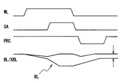
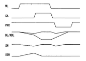
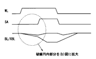
図2は一般的なSRAMの簡略化した回路構成の例を示し、図3はその主要信号の動作波形の一例を示す。また、図4(a)は、SRAMメモリセルからデータを読み出す際の、ワード線選択信号WLと、センスアンプ起動信号SA、及びビット線対の電位波形BL、XBLの例を示し、図4(b)は、センスアンプ起動時の、ビット線対の電位波形BL、XBLの波形拡大図を示す。図4(b)において、図中のAが、通常動作時の動作タイミングを示し、Bが、スクリーニング検査時の動作タイミングを示す。 FIG. 2 shows an example of a simplified circuit configuration of a general SRAM, and FIG. 3 shows an example of operation waveforms of main signals. FIG. 4A shows an example of the word line selection signal WL, the sense amplifier activation signal SA, and the potential waveforms BL and XBL of the bit line pair when data is read from the SRAM memory cell. b) is an enlarged waveform diagram of the potential waveforms BL and XBL of the bit line pair when the sense amplifier is activated. In FIG. 4B, A in the figure indicates the operation timing during the normal operation, and B indicates the operation timing during the screening test.
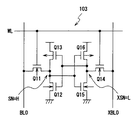
これらの図において、103はメモリセル、104はセンスアンプ、PRCはプリチャージ活性化信号、WLはワード線活性化信号、SAはセンスアンプ活性化信号(以下SA信号ともいう。)、BLは正論理側ビット線、XBLは負論理側ビット線、SNは正論理側メモリセル内部ノード、XSNは負論理側メモリセル内部ノード、Q11〜Q17はトランジスタである。 In these figures, 103 is a memory cell, 104 is a sense amplifier, PRC is a precharge activation signal, WL is a word line activation signal, SA is a sense amplifier activation signal (hereinafter also referred to as SA signal), and BL is positive. Logic side bit line, XBL is negative logic side bit line, SN is positive logic side memory cell internal node, XSN is negative logic side memory cell internal node, and Q11 to Q17 are transistors.
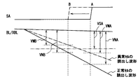
SA信号が、Aのタイミングで活性化されたとき、読出し電流能力が十分な正常セルの場合には、図4(b)の実線で示すように、この正常セルからの読出し電位差VNAは、センスアンプ104の検知レベルVSAより大きく、メモリセルからのデータを、センスアンプ104で検出することができる。
When the SA signal is activated at the timing A, in the case of a normal cell with sufficient read current capability, the read potential difference VNA from this normal cell is sensed as shown by the solid line in FIG. The
一方、SA信号がAのタイミングで活性化されたとき、工程中の異物等により読出し電流能力が少なくなった異常セルの場合には、この異常セルからの読出し電位VMAがセンスアンプ104の検知レベルより小さい時(図示せず)には、読み出しが行えずに異常セルは不良として検出されるが、図4(b)の一点鎖線で示すように、VNA>VMA>VSAである時には、この時点では正常読出しが行われてしまい、異常セルであることが初期検査で検出できない。
On the other hand, when the SA signal is activated at the timing A, the read potential VMA from the abnormal cell is detected by the
このような異常セルは、使用頻度が重なるにつれその特性が劣化し、時間の経過とともに信頼性不良に至ることが多く、特に市場不良となった場合には大きな問題となる。 Such an abnormal cell has its characteristics deteriorated as the use frequency overlaps, and it often leads to poor reliability over time, and becomes a serious problem especially when it becomes a bad market.
そこで、このような異常セルは、極力、初期検査時にスクリーニングすることが望ましい。これに対応するため、上記特許文献1に示される手法では、スクリーニング検査時に、センスアンプ104の起動タイミングをAからBに早めるようにしている。
Therefore, it is desirable to screen such an abnormal cell at the time of initial inspection as much as possible. In order to cope with this, in the method disclosed in
このように、センスアンプ104の起動タイミングを早めることにより、図4(b)からわかるように、異常セルからの読出し電位VMBは、センスアンプ検知レベルVSAより小さくなり、初期検査時に異常セルの検出が可能となる。
ところで、半導体集積回路装置の動作電圧の低電圧化により、SRAMの記憶ノードの安定性(以下、スタティックノイズマージン:SNMと略す)の確保が困難になり、読み出し動作時に、SRAMのデータを破壊してしまう“読みつぶし”を起こしやすくなる、という問題がある。この現象についての詳細は、IEEE JOURNAL OF SOLID−STATE CIRCUITS. VOL. SC−22,No.5, OCTOBER 1987 “Static−Noise Margin Analysis of MOS SRAM Cells”や電子情報通信学会論文誌C−II Vol.J75−C−II No.7 pp.350−361 1992年 7月“微細CMOSメモリセルのスタティックノイズマージン解析”などに示されている。 By the way, as the operating voltage of the semiconductor integrated circuit device is lowered, it becomes difficult to ensure the stability of the storage node of the SRAM (hereinafter abbreviated as static noise margin: SNM), and the SRAM data is destroyed during the read operation. There is a problem that it is easy to cause “reading crushing”. For more information on this phenomenon, see IEEE JOURNAL OF SOLID-STATE CIRCUITS. VOL. SC-22, No. 5, OCTOBER 1987 “Static-Noise Margin Analysis of MOS SRAM Cells” and IEICE Transactions C-II Vol. J75-C-II No. 7 pp. 350-361 July 1992 “Static noise margin analysis of fine CMOS memory cell”.
このように、半導体素子の微細化に伴う電源電圧の低下により、十分なSNM値を確保することが困難になってきており、更に製造工程で発生する異物等によりSRAMセルを構成するトランジスタの能力劣化が生じて、セル内のトランジスタ能力が設計値よりずれた場合には、SNM値は劣化し不良に至る。 As described above, it has become difficult to ensure a sufficient SNM value due to a decrease in power supply voltage accompanying the miniaturization of semiconductor elements, and further, the ability of a transistor constituting an SRAM cell due to foreign matter generated in the manufacturing process. When the deterioration occurs and the transistor capability in the cell deviates from the design value, the SNM value deteriorates and leads to a failure.
前述したように、このような製造工程で生じた異物による不具合は、この異常セルの使用頻度が重なるにつれその特性を劣化させるため、時間の経過とともに信頼性不良に至ることが多く、市場不良発生を未然に防ぐためにも、初期検査でスクリーニングすることが望ましい。 As described above, defects due to foreign matters generated in such a manufacturing process deteriorate the characteristics as the frequency of use of the abnormal cells overlaps, and thus often lead to poor reliability over time, resulting in market defects. In order to prevent this, it is desirable to screen at the initial inspection.
ここで、前述した従来の手法では、センスアンプの動作タイミングを早めることによりスクリーニングを行っているが、最近の半導体素子の低電圧化、及び高速化に伴い、センスアンプの動作タイミングは、ほとんどマージンの無い設計となっており、実質的に動作タイミングを早めることは、ほぼ不可能である。したがって、今後は、この手法によってSNM不足による信頼性不良を初期検査でスクリーニングすることは、事実上不可能な状態となっているものである。 Here, in the conventional method described above, screening is performed by accelerating the operation timing of the sense amplifier. However, with the recent reduction in voltage and speed of semiconductor elements, the operation timing of the sense amplifier is almost marginal. Therefore, it is almost impossible to substantially advance the operation timing. Therefore, in the future, it will be virtually impossible to screen for a reliability failure due to SNM shortage by an initial inspection by this method.
本発明は上記従来の課題に鑑みてなされたもので、SNM値不足による信頼性不良を、初期検査でスクリーニングすることのできる半導体記憶装置、及びその検査方法を提供することを目的としている。 The present invention has been made in view of the above-described conventional problems, and an object of the present invention is to provide a semiconductor memory device that can be screened for a reliability failure due to a shortage of SNM values by an initial test, and a test method therefor.
上記課題を解決するために、本発明の第1の半導体記憶装置は、SRAMを搭載した半導体記憶装置であって、前記SRAMのビット線対の各ビット線のそれぞれに通常動作用プリチャージ回路と検査用プリチャージ回路の各一端が並列接続されており、前記通常動作用プリチャージ回路と検査用プリチャージ回路とは同一の電源電圧に接続されており、前記ビット線対の各ビット線のそれぞれに接続された第1および第2の通常動作用プリチャージ回路は同一の第1の活性化信号で活性化され、前記ビット線対の一方のビット線に接続された第1の検査用プリチャージ回路は第2の活性化信号で活性化され、前記ビット線対の他方のビット線に接続された第2の検査用プリチャージ回路は第3の活性化信号で活性化され、前記第1乃至第3の各活性化信号は互いに独立に制御され、該半導体記憶装置の検査時において読出し動作前に、前記ビット線対の他方のビット線が第1のプリチャージ電位にある状態で、前記第2の活性化信号を活性化することにより、前記ビット線対の一方のビット線を第2のプリチャージ電位にして、または前記ビット線対の一方のビット線が前記1のプリチャージ電位にある状態で、前記第3の活性化信号を活性化することにより、前記ビット線対の他方のビット線を第2のプリチャージ電位にして、前記ビット線対の一方のビット線と前記ビット線対の他方のビット線とを互いに異なるプリチャージ電位までプリチャージするプリチャージ手段を、備えている。 In order to solve the above problems, a first semiconductor memory device of the present invention is a semiconductor memory device having an SRAM mounted thereon, and a normal operation precharge circuit is provided on each bit line of the SRAM bit line pair. Each end of the test precharge circuit is connected in parallel, and the normal operation precharge circuit and the test precharge circuit are connected to the same power supply voltage, and each bit line of the bit line pair The first and second normal operation precharge circuits connected to are activated by the same first activation signal and are connected to one bit line of the bit line pair. The circuit is activated by a second activation signal, and the second inspection precharge circuit connected to the other bit line of the bit line pair is activated by a third activation signal, and the first to Third The activation signals are controlled independently of each other, and the second activation line is in a state where the other bit line of the bit line pair is at the first precharge potential before the read operation at the time of inspection of the semiconductor memory device. By activating the enable signal, one bit line of the bit line pair is set to a second precharge potential, or one bit line of the bit line pair is at the precharge potential of 1, By activating the third activation signal, the other bit line of the bit line pair is set to a second precharge potential, and one bit line of the bit line pair and the other of the bit line pair are Precharge means for precharging the bit lines to different precharge potentials is provided.
また、本発明の第1の半導体記憶装置において、前記ビット線対の各ビット線の電位を設定するセンスアンプは、該半導体記憶装置の検査時において読出し動作前に、メモリセルに保持されているデータに応じて、前記ビット線対の一方のビット線をHまたはLレベルの所定の論理電位に設定し、その他方のビット線を、該一方のビット線に設定される論理電位とは相補型の論理電位に設定し、前記プリチャージ手段は、前記センスアンプにより前記ビット線対の他方のビット線が前記第1のプリチャージ電位と等しいHレベル論理電位に設定されているとき、前記第2の活性化信号を活性化して、Lレベル論理電位に設定されている一方のビット線を、前記Hレベル論理電位より低い第2のプリチャージ電位に充電し、前記センスアンプにより前記一方のビット線が前記第1のプリチャージ電位と等しいHレベル論理電位に設定されているとき、前記第3の活性化信号を活性化して、Lレベル論理電位に設定されている他方のビット線を、前記Hレベル論理電位より低い第2のプリチャージ電位に充電することが好ましい。 In the first semiconductor memory device of the present invention, the sense amplifier for setting the potential of each bit line of the bit line pair is held in the memory cell before the read operation at the time of inspection of the semiconductor memory device. Depending on the data, one bit line of the bit line pair is set to a predetermined logic potential of H or L level, and the other bit line is complementary to the logic potential set to the one bit line. When the other bit line of the bit line pair is set to an H level logical potential equal to the first precharge potential by the sense amplifier, the precharge means Is activated to charge one of the bit lines set to the L level logic potential to a second precharge potential lower than the H level logic potential, and to the sense amplifier. When the one bit line is set to the H level logic potential equal to the first precharge potential, the third activation signal is activated and the other bit line set to the L level logic potential is activated. It is preferable to charge the bit line to a second precharge potential lower than the H level logic potential.
また、本発明の第1の半導体記憶装置において、前記通常動作用プリチャージ回路および検査用プリチャージ回路は共にPチャネル型トランジスタからなり、前記プリチャージ手段は、前記検査用プリチャージ回路のPチャネル型トランジスタが、前記通常動作用プリチャージ回路のPチャネル型トランジスタより駆動能力が小さいトランジスタで構成されていることが好ましい。 In the first semiconductor memory device of the present invention, the normal operation precharge circuit and the test precharge circuit are both P-channel type transistors, and the precharge means includes a P channel of the test precharge circuit. The type transistor is preferably composed of a transistor having a smaller driving capability than the P-channel type transistor of the normal operation precharge circuit.
また、本発明の第1の半導体記憶装置において、前記通常動作用プリチャージ回路はPチャネル型トランジスタからなり、前記検査用プリチャージ回路はNチャネル型トランジスタからなり、前記ビット線対の一方のビット線と前記ビット線対の他方のビット線とを互いに異なるプリチャージ電位までプリチャージする手段は、前記通常動作用プリチャージ回路が接続されたビット線には第1のプリチャージ電位が印加され、前記検査用プリチャージ回路が接続されたビット線には前記第1のプリチャージ電位よりも前記Nチャネル型トランジスタの閾値電圧分低い第2のプリチャージ電位が印加されることが好ましい。 In the first semiconductor memory device of the present invention, the normal operation precharge circuit is formed of a P-channel transistor, the inspection precharge circuit is formed of an N-channel transistor, and one bit of the bit line pair Means for precharging the line and the other bit line of the bit line pair to different precharge potentials, the first precharge potential is applied to the bit line connected to the normal operation precharge circuit; It is preferable that a second precharge potential that is lower than the first precharge potential by the threshold voltage of the N-channel transistor is applied to the bit line to which the inspection precharge circuit is connected.
また、本発明の第2の半導体記憶装置は、SRAMを搭載した半導体記憶装置であって、前記SRAMのビット線対の各ビット線のそれぞれに通常動作用プリチャージ回路と検査用プリチャージ回路の各一端が並列接続されており、前記通常動作用プリチャージ回路は、第1の電源電圧に接続されており、前記検査用プリチャージ回路は前記第1の電源電圧よりも低い第2の電源電圧に接続されており、前記ビット線対の一方のビット線に接続された通常動作用プリチャージ回路は第1の活性化信号で活性化され、前記ビット線対の他方のビット線に接続された通常動作用プリチャージ回路は第2の活性化信号で活性化され、前記ビット線対の一方のビット線に接続された検査用プリチャージ回路は第3の活性化信号で活性化され、前記ビット線対の他方のビット線に接続された検査用プリチャージ回路は第4の活性化信号で活性化され、前記第1乃至第4の各活性化信号は互いに独立に制御され、該半導体記憶装置の検査時において読出し動作前に、前記第1および第4の活性化信号を活性化するか、または前記第2および第3の活性化信号を活性化することにより、前記ビット線対の一方のビット線と前記ビット線対の他方のビット線とを互いに異なるプリチャージ電位までプリチャージするプリチャージ手段を備えている。 A second semiconductor memory device according to the present invention is a semiconductor memory device having an SRAM mounted thereon, wherein a normal operation precharge circuit and a test precharge circuit are provided for each bit line of the SRAM bit line pair. Each one end is connected in parallel, the normal operation precharge circuit is connected to a first power supply voltage, and the test precharge circuit is a second power supply voltage lower than the first power supply voltage. The normal operation precharge circuit connected to one bit line of the bit line pair is activated by a first activation signal and connected to the other bit line of the bit line pair. The normal operation precharge circuit is activated by the second activation signal, and the inspection precharge circuit connected to one bit line of the bit line pair is activated by the third activation signal. The test precharge circuit connected to the other bit line of the line pair is activated by a fourth activation signal, and the first to fourth activation signals are controlled independently of each other, and the semiconductor memory device When the first and fourth activation signals are activated or the second and third activation signals are activated before the read operation at the time of the inspection, one of the bit line pairs is activated. Precharge means for precharging the bit line and the other bit line of the bit line pair to different precharge potentials is provided.
また、本発明の第2の半導体記憶装置において、前記通常動作用プリチャージ回路および検査用プリチャージ回路は共にPチャネル型トランジスタからなり、前記プリチャージ手段は、前記検査用プリチャージ回路のPチャネル型トランジスタと前記通常動作用プリチャージ回路のPチャネル型トランジスタとが駆動能力が等しいトランジスタで構成されていることが好ましい。 In the second semiconductor memory device of the present invention, the normal operation precharge circuit and the test precharge circuit are both P-channel type transistors, and the precharge means includes a P channel of the test precharge circuit. The type transistor and the P-channel type transistor of the normal operation precharge circuit are preferably composed of transistors having the same driving capability.
また、本発明の第3の半導体記憶装置は、SRAMを搭載した半導体記憶装置であって、前記SRAMのビット線対の各ビット線のそれぞれに通常動作用プリチャージ回路と検査用プリチャージ回路の各一端が並列接続されており、前記通常動作用プリチャージ回路と検査用プリチャージ回路とは同一の電源電圧に接続されており、前記ビット線対の一方のビット線に接続された通常動作用プリチャージ回路は第1の活性化信号で活性化され、前記ビット線対の他方のビット線に接続された通常動作用プリチャージ回路は第2の活性化信号で活性化され、前記ビット線対の一方のビット線に接続された検査用プリチャージ回路は第1のレベルシフト回路を介して第3の活性化信号で活性化され、前記ビット線対の他方のビット線に接続された検査用プリチャージ回路は第2のレベルシフト回路を介して第4の活性化信号で活性化され、前記第1乃至第4の各活性化信号は互いに独立に制御され、該半導体記憶装置の検査時において読出し動作前に、前記第1および第4の活性化信号を活性化するか、または前記第2および第3の活性化信号を活性化することにより、前記ビット線対の一方のビット線と前記ビット線対の他方のビット線とを互いに異なるプリチャージ電位までプリチャージするプリチャージ手段を備えている。 A third semiconductor memory device according to the present invention is a semiconductor memory device having an SRAM mounted thereon, wherein a normal operation precharge circuit and a test precharge circuit are provided on each bit line of the SRAM bit line pair. Each one end is connected in parallel, the normal operation precharge circuit and the test precharge circuit are connected to the same power supply voltage, and are connected to one bit line of the bit line pair for normal operation The precharge circuit is activated by the first activation signal, the normal operation precharge circuit connected to the other bit line of the bit line pair is activated by the second activation signal, and the bit line pair is activated. The precharge circuit for inspection connected to one of the bit lines is activated by the third activation signal via the first level shift circuit and connected to the other bit line of the bit line pair. The inspection precharge circuit is activated by the fourth activation signal through the second level shift circuit, and the first to fourth activation signals are controlled independently of each other, and the semiconductor memory device is inspected. In some cases, before the read operation, by activating the first and fourth activation signals or activating the second and third activation signals, one bit line of the bit line pair And precharge means for precharging the other bit line of the bit line pair to different precharge potentials.
また、本発明の第3の半導体記憶装置において、前記通常動作用プリチャージ回路および検査用プリチャージ回路は共にPチャネル型トランジスタからなり、前記プリチャージ手段は、前記第1または第2のレベルシフト回路により前記検査用プリチャージ回路のPチャネル型トランジスタの駆動能力が前記通常動作用プリチャージ回路のPチャネル型トランジスタの駆動能力より小さくなるように制御することが好ましい。 In the third semiconductor memory device of the present invention, both of the normal operation precharge circuit and the test precharge circuit are P-channel transistors, and the precharge means includes the first or second level shifter. It is preferable to control the driving capability of the P-channel transistor of the inspection precharge circuit to be smaller than the driving capability of the P-channel transistor of the normal operation precharge circuit.
また、本発明の第4の半導体記憶装置は、SRAMを搭載した半導体記憶装置であって、前記SRAMのビット線対の各ビット線のそれぞれ第1および第2のプリチャージ回路が接続されており、前記各プリチャージ回路は同一の電源電圧に接続されており、前記ビット線対の一方のビット線に接続された第1のプリチャージ回路は第1のレベルシフト回路を介して第1の活性化信号で活性化され、前記ビット線対の他方のビット線に接続された第2のプリチャージ回路は第2のレベルシフト回路を介して第2の活性化信号で活性化され、前記第1および第2の各活性化信号は互いに独立に制御され、前記第1および第2のプリチャージ回路の通常動作モードと検査動作モードの切替えは前記第1および第2のレベルシフト回路を制御する制御回路によって行なわれ、該半導体記憶装置の検査時において読出し動作前に、前記第1および第2の活性化信号を活性化することにより、前記ビット線対の一方のビット線と前記ビット線対の他方のビット線とを互いに異なるプリチャージ電位までプリチャージするプリチャージ手段を備えている。 The fourth semiconductor memory device according to the present invention is a semiconductor memory device having an SRAM mounted thereon, to which the first and second precharge circuits of each bit line of the SRAM bit line pair are connected. The precharge circuits are connected to the same power supply voltage, and the first precharge circuit connected to one bit line of the bit line pair has a first active level via a first level shift circuit. The second precharge circuit activated by the activation signal and connected to the other bit line of the bit line pair is activated by the second activation signal via the second level shift circuit, and The second activation signal and the second activation signal are controlled independently of each other, and switching between the normal operation mode and the inspection operation mode of the first and second precharge circuits is a control for controlling the first and second level shift circuits. By activating the first and second activation signals before the read operation at the time of testing the semiconductor memory device, the one bit line of the bit line pair and the bit line pair are Precharge means for precharging the other bit line to different precharge potentials is provided.
また、本発明の第4の半導体記憶装置において、前記各プリチャージ回路はPチャネル型トランジスタからなり、前記プリチャージ手段は、前記第1および第2のレベルシフト回路により前記各プリチャージ回路の一方のPチャネル型トランジスタの駆動能力が前記各プリチャージ回路の他方のPチャネル型トランジスタの駆動能力よりも小さくなるよう制御することが好ましい。 In the fourth semiconductor memory device of the present invention, each of the precharge circuits is composed of a P-channel transistor, and the precharge means is connected to one of the precharge circuits by the first and second level shift circuits. It is preferable to control so that the drive capability of the P-channel transistor is smaller than the drive capability of the other P-channel transistor of each precharge circuit.
また、本発明の第5の半導体記憶装置は、SRAMを搭載した半導体記憶装置であって、前記SRAMのビット線対の各ビット線のそれぞれに第1および第2のプリチャージ回路が接続されており、前記各プリチャージ回路は同一の電源電圧に接続されており、前記ビット線対の一方のビット線に接続された第1のプリチャージ回路は第1の遅延回路を介して第1の活性化信号で活性化され、前記ビット線対の他方のビット線に接続された第2のプリチャージ回路は第2の遅延回路を介して第2の活性化信号で活性化され、前記第1および第2の各活性化信号は互いに独立に制御され、前記プリチャージ回路の通常動作モードと検査動作モードの切替えは、前記第1および第2の遅延回路を制御する制御回路によって行なわれ、該半導体装置の検査時において読出し動作前に、前記第1および第2の活性化信号を活性化することにより、前記ビット線対の一方のビット線と前記ビット線対の他方のビット線とを互いに異なるプリチャージ電位までプリチャージするプリチャージ手段を備えている。 The fifth semiconductor memory device of the present invention is a semiconductor memory device having an SRAM mounted thereon, and first and second precharge circuits are connected to each bit line of the SRAM bit line pair. Each of the precharge circuits is connected to the same power supply voltage, and the first precharge circuit connected to one bit line of the bit line pair has a first active circuit via a first delay circuit. A second precharge circuit activated by an activation signal and connected to the other bit line of the bit line pair is activated by a second activation signal via a second delay circuit, and The second activation signals are controlled independently of each other, and switching between the normal operation mode and the inspection operation mode of the precharge circuit is performed by a control circuit that controls the first and second delay circuits. apparatus By activating the first and second activation signals at the time of inspection before the read operation, one bit line of the bit line pair and the other bit line of the bit line pair are precharged differently. Precharge means for precharging to potential is provided.
また、本発明の第5の半導体記憶装置において、前記各プリチャージ回路はPチャネル型トランジスタからなり、前記プリチャージ手段は、前記第1および第2の遅延回路により、前記各プリチャージ回路の一方のPチャネル型トランジスタの立ち上がり動作を前記各プリチャージ回路の他方のPチャネル型トランジスタの立ち上がり動作より早めて、前記各プリチャージ回路の一方のPチャネル型トランジスタのプリチャージが不十分な状態でプリチャージ動作を完了させることが好ましい。 Further, in the fifth semiconductor memory device of the present invention, each precharge circuit is formed of a P-channel transistor, and the precharge means includes one of the precharge circuits by the first and second delay circuits. The rising operation of the P-channel transistor of each precharge circuit is advanced earlier than the rising operation of the other P-channel transistor of each precharge circuit, and the precharge of one P-channel transistor of each precharge circuit is insufficient. It is preferable to complete the charging operation.
また、本発明の第1の半導体記憶装置の検査方法は、本発明の第1の半導体記憶装置を用いた半導体記憶装置の検査方法であって、前記第1または第2の通常動作用プリチャージ回路が接続された前記ビット線対の一方のビット線に第1のプリチャージ電位を印加し、前記第1または第2の検査用プリチャージ回路が接続された前記ビット線対の他方のビット線に前記第1のプリチャージ電位より低い第2のプリチャージ電位を印加する第1の工程と、前記第1の工程の後に読出し動作を行なって動作マージン検査を行う第2の工程とを有する。 A first semiconductor memory device inspection method according to the present invention is a semiconductor memory device inspection method using the first semiconductor memory device according to the present invention, wherein the first or second normal operation precharge is performed. A first precharge potential is applied to one bit line of the bit line pair to which the circuit is connected, and the other bit line of the bit line pair to which the first or second test precharge circuit is connected A first step of applying a second precharge potential lower than the first precharge potential, and a second step of performing an operation margin inspection by performing a read operation after the first step.
また、本発明の第2の半導体記憶装置の検査方法は、本発明の第2の半導体記憶装置を用いた半導体記憶装置の検査方法であって、前記第1または第2の通常動作用プリチャージ回路が接続された前記ビット線対の一方のビット線に前記第1の電源電圧を印加し、前記第1または第2の検査用プリチャージ回路が接続された前記ビット線対の他方のビット線に前記第2の電源電圧を印加する第1の工程と、前記第1の工程の後に読出し動作を行なって動作マージン検査を行う第2の工程とを有する。 A second semiconductor memory device inspection method of the present invention is a semiconductor memory device inspection method using the second semiconductor memory device of the present invention, wherein the first or second normal operation precharge is performed. The first power supply voltage is applied to one bit line of the bit line pair to which the circuit is connected, and the other bit line of the bit line pair to which the first or second test precharge circuit is connected A first step of applying the second power supply voltage, and a second step of performing an operation margin inspection by performing a read operation after the first step.
また、本発明の第3の半導体記憶装置の検査方法は、本発明の第3の半導体記憶装置を用いた半導体記憶装置の検査方法であって、前記第1または第2の通常動作用プリチャージ回路が接続された前記ビット線対の一方のビット線に電源電圧を印加し、前記第1または第2の検査用プリチャージ回路が接続された前記ビット線対の他方のビット線に、前記第1または第2のレベルシフト回路によって前記電源電圧よりも低く設定された電位を印加する第1の工程と、前記第1の工程の後に読出し動作を行なって動作マージン検査を行う第2の工程とを有する。 A third semiconductor memory device inspection method of the present invention is a semiconductor memory device inspection method using the third semiconductor memory device of the present invention, wherein the first or second normal operation precharge is performed. A power supply voltage is applied to one bit line of the bit line pair connected to the circuit, and the second bit line of the bit line pair connected to the first or second test precharge circuit is connected to the first bit line. A first step of applying a potential set lower than the power supply voltage by the first or second level shift circuit; and a second step of performing a read operation after the first step to perform an operation margin inspection. Have
また、本発明の第4の半導体記憶装置の検査方法は、本発明の第4の半導体記憶装置を用いた半導体記憶装置の検査方法であって、前記第2のプリチャージ回路が接続された前記ビット線対の他方のビット線に電源電圧を印加し、前記第1のプリチャージ回路が接続された前記ビット線対の一方のビット線に前記第1および第2のレベルシフト回路によって前記電源電圧よりも低く設定された電位を印加する第1の工程と、前記第1の工程の後に読出し動作を行なって動作マージン検査を行う第2の工程とを有する。 The fourth semiconductor memory device inspection method of the present invention is a semiconductor memory device inspection method using the fourth semiconductor memory device of the present invention, wherein the second precharge circuit is connected to the semiconductor memory device. A power supply voltage is applied to the other bit line of the bit line pair, and the power supply voltage is applied to one bit line of the bit line pair to which the first precharge circuit is connected by the first and second level shift circuits. A first step of applying a potential set lower than the first step, and a second step of performing an operation margin inspection by performing a read operation after the first step.
また、本発明の第5の半導体記憶装置の検査方法は、本発明の第5の半導体記憶装置を用いた半導体記憶装置の検査方法であって、前記第2のプリチャージ回路を第2の遅延回路を介して第2の活性化信号により活性化して、前記第2のプリチャージ回路が接続された前記ビット線対の他方のビット線に電源電圧を印加し、前記第1のプリチャージ回路を第1の遅延回路を介して第1の活性化信号により活性化し、前記第1のプリチャージ回路の立ち上がり動作を前記第1の遅延回路によって前記第2のプリチャージ回路の立ち上がり動作よりも早めて、プリチャージが不十分な状態で該プリチャージ動作を完了して、前記第1のプリチャージ回路が接続された前記ビット線対の一方のビット線に、前記電源電圧よりも低い電位を印加する第1の工程と、前記第1の工程の後に読出し動作を行なって動作マージン検査を行う第2の工程とを有する。 The fifth semiconductor memory device inspection method of the present invention is a semiconductor memory device inspection method using the fifth semiconductor memory device of the present invention, wherein the second precharge circuit is connected to the second delay circuit. Activated by a second activation signal through a circuit, a power supply voltage is applied to the other bit line of the bit line pair to which the second precharge circuit is connected, and the first precharge circuit is It is activated by a first activation signal through a first delay circuit, and the rising operation of the first precharge circuit is made earlier than the rising operation of the second precharge circuit by the first delay circuit. The precharge operation is completed with insufficient precharge, and a potential lower than the power supply voltage is applied to one bit line of the bit line pair to which the first precharge circuit is connected. First Having between step and a second step of performing an operation margin test performs a read operation after the first step.
本発明に係る半導体記憶装置、およびその検査方法によれば、通常動作ではスクリーニングできない、工程不良等によるSNM値不足による信頼性不良を、初期検査でスクリーニングすることができる。 According to the semiconductor memory device and the inspection method thereof according to the present invention, it is possible to screen a reliability failure due to a shortage of an SNM value due to a process failure or the like, which cannot be screened by a normal operation, by an initial inspection.
本発明の実施の形態について述べる前に、SNM値不足による“読みつぶし”不良について図面を参照しながら説明する。 Before describing the embodiment of the present invention, “read-out” failure due to lack of SNM value will be described with reference to the drawings.
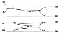
SNM値不足による“読みつぶし”不良と、本発明の全ての実施の形態に共通する作用効果について、図5(a)〜図5(d)を参照しながら説明する。 The “read-out” failure due to the shortage of the SNM value and the effects common to all the embodiments of the present invention will be described with reference to FIGS. 5 (a) to 5 (d).
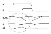
図5(a)は、図3と同じく、SRAMメモリセルの動作時の各信号波形を示し、破線の円で囲んだ部分の波形を拡大したものを、図5(b)〜図5(d)に示す。 FIG. 5A shows each signal waveform during the operation of the SRAM memory cell, as in FIG. 3, and shows an enlarged waveform of a portion surrounded by a broken-line circle, which is shown in FIGS. 5B to 5D. ).
図5(b)のBL/XBLは、ビット線対の波形を示す。この図では、実線がBLを示し、破線がXBLを示す。また、BL=“H”であり、メモリセルに“1”のデータが蓄えられているものとする。SN,XSNは、メモリセルの内部ノードの波形を示し、SN=“H”、XSN=“L”である。 BL / XBL in FIG. 5B indicates the waveform of the bit line pair. In this figure, a solid line indicates BL and a broken line indicates XBL. Further, it is assumed that BL = “H” and data “1” is stored in the memory cell. SN and XSN indicate waveforms of internal nodes of the memory cell, and SN = “H” and XSN = “L”.
正常セルの場合、SN,XSNの波形は、実線で示したような波形となる。一方、前述のようなSNM値が不足したメモリセルの内部ノードの波形SN,XSNは、一点鎖線と破線で示すようになり、正常セルの実線波形に比べ、両者間の電位差が小さくなる。このような不良モードは、実使用時間の経過とともに、劣化が進み、図5(c)のように、内部ノードの電位差が無くなり、最終的に読出し不良に至ってしまう。 In the case of a normal cell, the waveforms of SN and XSN are as shown by solid lines. On the other hand, the waveforms SN and XSN of the internal node of the memory cell having a shortage of the SNM value as described above are as indicated by the alternate long and short dash line and the broken line, and the potential difference between the two becomes smaller than that of the normal cell. Such a failure mode deteriorates as the actual usage time elapses, and as shown in FIG. 5C, there is no potential difference between the internal nodes, and eventually a read failure occurs.
このような信頼性不良は、初期検査時にスクリーニングすることが望ましい。そこで、本発明において、初期検査時にスクリーニングする手段について、以下に述べる。 Such poor reliability is desirably screened at the initial inspection. Therefore, in the present invention, means for screening at the initial inspection will be described below.
本発明では、図5(d)に示すように、読出し開始直前に“L”データを保存する内部ノードXSNにつながるビット線XBLの電位を、対となるビット線BLより高めに設定する。しかる後に、読出し動作を始めると、上記従来回路では、図5(b)に示すような、初期状態でSNM値が小さいメモリセルの“L”側ノードである、破線で示されるXSNの内部波形は、図5(b)に示すように低い電圧であったが、本発明回路では、その接続するビット線XBLの初期電位が上記のように高めに設定されていることから、図5(d)の破線で示すように、従来回路で読み出す場合より、電位が高くなる。この結果、対となるSNの電位は、相対的に低くなり、結果として、図5(d)に示されるように、より評価初期において、図5(c)に示す電位差が無くなった状態にすることが可能となり、早期に誤動作に至らせることができ、通常動作ではスクリーニングできないSNM値不足のメモリセルを、初期状態で不良と判定することができる。 In the present invention, as shown in FIG. 5D, the potential of the bit line XBL connected to the internal node XSN storing “L” data is set higher than that of the paired bit line BL immediately before the start of reading. Thereafter, when the read operation is started, in the conventional circuit, the internal waveform of the XSN indicated by the broken line, which is the “L” side node of the memory cell having a small SNM value in the initial state, as shown in FIG. Is a low voltage as shown in FIG. 5B, but in the circuit of the present invention, since the initial potential of the bit line XBL to be connected is set higher as described above, FIG. ), The potential is higher than in the case of reading with a conventional circuit. As a result, the potential of the paired SN is relatively low, and as a result, as shown in FIG. 5D, the potential difference shown in FIG. Thus, a malfunctioning memory can be brought to an early stage, and a memory cell having a shortage of SNM values that cannot be screened by normal operation can be determined to be defective in the initial state.
以上のことから、読み出し前に、ビット線対の一方のビット線と、他方のビット線に互いに異なるプリチャージ電位を与えた後、読出し検査を行うことで、従来、初期不良として検出できなかったSNM値不足のメモリセルを、初期状態で不良と判定することができるようになる。 From the above, conventionally, it was not possible to detect as an initial failure by performing a read inspection after applying different precharge potentials to one bit line of the bit line pair and the other bit line before reading. A memory cell having an insufficient SNM value can be determined to be defective in the initial state.
(実施の形態1)
以下、本発明の実施の形態1による半導体記憶装置について、図面を参照しながら説明する。
(Embodiment 1)
The semiconductor memory device according to the first embodiment of the present invention will be described below with reference to the drawings.
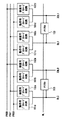
図1(a)は、本発明の実施の形態1による半導体記憶装置の回路構成を示す図、図1(b)は、該半導体記憶装置を構成するメモリセルの回路構成を示す図、図1(c)は、該半導体記憶装置における主要信号の動作波形の一例を示す図である。 1A is a diagram showing a circuit configuration of a semiconductor memory device according to the first embodiment of the present invention, FIG. 1B is a diagram showing a circuit configuration of memory cells constituting the semiconductor memory device, and FIG. (C) is a figure which shows an example of the operation | movement waveform of the main signal in this semiconductor memory device.
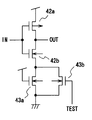
図1において、図2及び図3と同一符号は、従来の半導体記憶装置におけるものと同一のものを示し、101a〜101dは通常動作用プリチャージ回路、102a〜102dはスクリーニング検査用プリチャージ回路、PRC0は、通常動作用プリチャージ回路101a〜101dの活性化信号(第1の活性化信号であり、以下、PRC0信号ともいう。)、PRCTは、正論理側ビット線BL0,BL1につながる検査用プリチャージ回路102a,102cの活性化信号(第2の活性化信号であり、以下、PRCT信号ともいう。)、PRCBは、負論理側ビット線BLX0,BLX1につながる検査用プリチャージ回路102b,102dの活性化信号(第3の活性化信号であり、以下、PRCB信号ともいう。)である。
1, the same reference numerals as those in FIGS. 2 and 3 denote the same components as those in the conventional semiconductor memory device, 101a to 101d are precharge circuits for normal operation, 102a to 102d are precharge circuits for screening tests, PRC0 is an activation signal for the normal
以下、本実施の形態1の半導体記憶装置の構成を、より詳細に説明する。
まず、本実施の形態1の半導体記憶装置は、図1(a)に示すように、ビット線対をプリチャージするためのプリチャージ回路として、正論理側ビット線BL、負論理側ビット線XBLの各ビット線ごとに、2つのプリチャージ回路、つまり通常動作時用のプリチャージ回路101a,101b,101c,101dと、スクリーニング検査時用のプリチャージ回路102a,102b,102c,102dとを有する。
Hereinafter, the configuration of the semiconductor memory device according to the first embodiment will be described in more detail.
First, as shown in FIG. 1A, the semiconductor memory device of the first embodiment has a positive logic side bit line BL and a negative logic side bit line XBL as precharge circuits for precharging bit line pairs. Each bit line includes two precharge circuits, that is,
それぞれのビット線BL0,XBL0,BL1,XBL1につながる通常動作用のプリチャージ回路101a,101b,101c,101dは、通常動作用のプリチャージ起動信号PRC0=“L”(第1の活性化信号)によって活性化され、ビット線を、“H”=“Vdd”状態にプリチャージする。正論理側ビット線BL0,BL1につながるスクリーニング検査時用プリチャージ回路102a,102cは、正論理ビット線プリチャージ回路活性化信号PRCT(第2の活性化信号)により活性化され、該正論理側ビット線のプリチャージ動作を行う。負論理側ビット線XBL0,XBL1につながるスクリーニング検査時用プリチャージ102b,102dは、負論理ビット線プリチャージ回路活性化信号PRCB(第3の活性化信号)によって活性化し、該負論理側ビット線をプリチャージする。ここで、スクリーニング検査用プリチャージ回路102a〜102dは、通常動作用プリチャージ回路101a〜101dとは、異なる電位までビット線をプリチャージする機能を有する回路で構成されている。
The normal
また、図1(b)において、メモリセル103において、Q11、Q12、Q13、Q14、Q15、Q16は、メモリセル103を構成するトランジスタである。
In FIG. 1B, in the
次に、本実施の形態1の半導体記憶装置の動作について説明する。
通常の動作時には、PRC0信号(第1の活性化信号)のみが活性化し、通常動作用プリチャージ回路101a〜101dのみが動作して、図3に示したように、ビット線対を、読出し動作前に“H”=“Vdd”状態にプリチャージする。
Next, the operation of the semiconductor memory device according to the first embodiment will be described.
During normal operation, only the PRC0 signal (first activation signal) is activated, and only the normal
次に、SNM不足ビットをスクリーニングする、スクリーニング検査時の動作について説明する。
この検査時には、ビット線対の、メモリセル内部の“L”データが保持されるノードにつながるビット線を第1のプリチャージ電位にプリチャージし、該ビット線対の、メモリセル内部の“H”データが保持されるノードにつながるビット線を第1のプリチャージ電位より低い第2のプリチャージ電位にプリチャージする。
Next, the operation at the screening test for screening SNM deficient bits will be described.
At the time of this inspection, the bit line connected to the node holding the “L” data in the memory cell in the bit line pair is precharged to the first precharge potential, and the “H” in the memory cell in the bit line pair is precharged. “The bit line connected to the data holding node is precharged to a second precharge potential lower than the first precharge potential.
たとえば、メモリセル103が“1”のデータを保持している時、内部ノードSNが“H”状態で、相補側ノードXSNは“L”の状態になっていたとする。
For example, assume that when the
該当セルデータを読み出すのに先立って、該当セルの保持するデータとは相補型のデータをビット線上に読み出す。つまり、正論理側ビット線BL0に、正論理側内部ノードSNに保持される“H”状態とは相補型の“L”データを読出し、負論理側ビット線XBL0には、負論理側内部ノードXSNの“L”データと相補型の“H”データを読み出す。これは、半導体記憶装置の検査で通常用いられる検査パターンの1つ、例えば“チェッカーパターン”などのように“H”、“L”を交互に書込み/読出しを行う検査パターンを用いれば容易に行える。これにより、正論理側ビット線BL0は“L”状態となり、負論理側ビット線XBL0は“H”状態となる。このとき、“H”状態のビット線の電位は、通常の“H”=“Vdd”電位であり、これは第1のプリチャージ電位と等しい。 Prior to reading the corresponding cell data, data complementary to the data held in the corresponding cell is read onto the bit line. That is, “L” data complementary to the “H” state held in the positive logic side internal node SN is read out to the positive logic side bit line BL0, and the negative logic side internal node is connected to the negative logic side bit line XBL0. Read XSN “L” data and complementary “H” data. This can be easily performed by using an inspection pattern in which “H” and “L” are alternately written / read, such as one of the inspection patterns normally used in the inspection of the semiconductor memory device, for example, “checker pattern”. . As a result, the positive logic side bit line BL0 is in the “L” state, and the negative logic side bit line XBL0 is in the “H” state. At this time, the potential of the bit line in the “H” state is a normal “H” = “Vdd” potential, which is equal to the first precharge potential.
この後、正論理側プリチャージ回路活性信号PRCTを活性化することにより、“L”状態のBL0をプリチャージする。このとき、スクリーニング検査用プリチャージ回路102は、通常の“H”=“Vdd”電位より低い電位までプリチャージする機能を有しているので、正論理側ビット線BL0は“H”より低い電位である第2のプリチャージ電位となる。また、負論理側ビット線XBL0は直前の読出し動作でセンスアンプにより電位が前記第1のプリチャージ電位と等しい“H”=“Vdd”となっているので、特にプリチャージする必要はない。 Thereafter, the positive logic side precharge circuit activation signal PRCT is activated to precharge BL0 in the “L” state. At this time, since the screening test precharge circuit 102 has a function of precharging to a potential lower than the normal “H” = “Vdd” potential, the positive logic side bit line BL 0 has a potential lower than “H”. Is the second precharge potential. The negative logic side bit line XBL0 does not need to be precharged because the potential is equal to the first precharge potential “H” = “Vdd” by the sense amplifier in the immediately preceding read operation.
これにより、ビット線対BL0/XBL0には、スクリーニング検査用プリチャージ回路102によって設定される電位差が生じる。この後に、通常と同じように読出し動作を行えば、前述のようにSNM値がセンスアンプの検知レベルに対してマージンの少ないメモリセル103では誤読み出しが行なわれ、不良と判定されてスクリーニングされることになる。
As a result, a potential difference set by the screening test precharge circuit 102 is generated in the bit line pair BL0 / XBL0. Thereafter, if the read operation is performed in the same manner as usual, as described above, the SNM value is erroneously read in the
一方、メモリセルの負論理側ノードXSNに“H”を書き込んだメモリセル103が“0”のデータを保持している場合には、負論理側プリチャージ回路活性信号PRCBを活性化することで、同様に検査できる。
On the other hand, when the
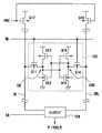
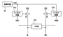
次に、プリチャージ回路のより詳細な内容を、図7に示す。通常動作用のプリチャージ起動信号PRC0(第1の活性化信号)には、通常動作用プリチャージ回路101a,101bをそれぞれ構成するプリチャージ用トランジスタQ1、Q2がつながっており、ビット線対を電源電位“Vdd”にプリチャージする。スクリーニング検査時用プリチャージ活性化信号PRCT/PRCB(第2、第3の活性化信号)には、スクリーニング検査用プリチャージ回路102a,102bをそれぞれ構成するトランジスタQ3、Q4がつながっており、ビット線対を電源電位“Vdd”にプリチャージする(すなわち、これらの信号PRCT/PRCBは“L”=“Vss”状態でビット線対をプリチャージし、“H”=“Vdd”状態でビット線対をプリチャージしない)。
Next, more detailed contents of the precharge circuit are shown in FIG. The normal operation precharge activation signal PRC0 (first activation signal) is connected to the precharge transistors Q1 and Q2 constituting the normal
これら4個のトランジスタの駆動能力は、Q1=Q2>Q3=Q4と設定され、Q1、Q2のトランジスタは通常の動作時のプリチャージ動作に十分な駆動能力を有するが、Q3、Q4のトランジスタはQ1、Q2に比べて駆動能力が小さく、通常の動作タイミングではビット線を十分に“H”=“Vdd”レベルまでプリチャージする駆動能力を有さない。このため、スクリーニング検査時には、Q3、Q4のトランジスタを使用することでビット線対に電位差を生じさせることができる。 The drive capability of these four transistors is set as Q1 = Q2> Q3 = Q4, and the transistors of Q1 and Q2 have sufficient drive capability for precharge operation during normal operation, but the transistors of Q3 and Q4 The driving capability is smaller than Q1 and Q2, and the driving capability to precharge the bit line sufficiently to “H” = “Vdd” level is not provided at the normal operation timing. Therefore, a potential difference can be generated in the bit line pair by using the transistors Q3 and Q4 during the screening test.
これにより、本実施の形態1においては、通常の検査では不良と判定されないSNM値不足のメモリセル103を、スクリーニング検査によってスクリーニングすることが可能となり、かかる検査を行った半導体記憶装置の市場での信頼性を向上することができる。
As a result, in the first embodiment, it becomes possible to screen the
このように、本実施の形態1による半導体記憶装置によれば、SRAMを搭載した半導体記憶装置において、SRAMのビット線対の各ビット線のそれぞれに通常動作用プリチャージ回路と検査用プリチャージ回路の各一端を並列接続し、通常動作用プリチャージ回路と検査用プリチャージ回路とは同一の電源電圧に接続し、ビット線対の各ビット線のそれぞれに接続した通常動作用プリチャージ回路は同一の第1の活性化信号で活性化し、ビット線対の一方のビット線に接続した検査用プリチャージ回路は第2の活性化信号で活性化し、ビット線対の他方のビット線に接続した検査用プリチャージ回路は第3の活性化信号で活性化し、第1乃至第3の各活性化信号は互いに独立に制御されるものとし、検査時においては、読出し動作前に、前記ビット線対の他方または一方のビット線が第1のプリチャージ電位にある状態で、前記第2または第3の活性化信号を活性化することによって、前記ビット線対の一方または他方のビット線を第2のプリチャージ電位にして、ビット線対の一方のビット線と、ビット線対の他方のビット線とを、互いに異なるプリチャージ電位までプリチャージするようにしたので、通常動作ではスクリーニングできない工程不良等によるSNM値不足による信頼性不良を、初期検査でスクリーニングすることができる効果が得られる。 As described above, according to the semiconductor memory device according to the first embodiment, in the semiconductor memory device mounting the SRAM, the normal operation precharge circuit and the test precharge circuit are provided for each bit line of the SRAM bit line pair. The normal operation precharge circuit and the inspection precharge circuit are connected to the same power supply voltage, and the normal operation precharge circuit connected to each bit line of the bit line pair is the same. The test precharge circuit that is activated by the first activation signal and connected to one bit line of the bit line pair is activated by the second activation signal and is connected to the other bit line of the bit line pair The precharge circuit for use is activated by the third activation signal, and the first to third activation signals are controlled independently of each other. At the time of inspection, before the read operation, One or the other bit of the bit line pair is activated by activating the second or third activation signal in a state where the other or one bit line of the bit line pair is at the first precharge potential. Since the line is set to the second precharge potential and one bit line of the bit line pair and the other bit line of the bit line pair are precharged to different precharge potentials, screening is performed in normal operation. An effect is obtained in which a reliability failure due to a shortage of SNM values due to a process failure that cannot be performed can be screened in an initial inspection.
(実施の形態2)
以下、本発明の実施の形態2による半導体記憶装置について、図面を参照しながら説明する。
本実施の形態2の半導体記憶装置の基本的回路構成は、上記実施の形態1と同じ図1で表されるため、その説明は省略する。
(Embodiment 2)
Hereinafter, a semiconductor memory device according to a second embodiment of the present invention will be described with reference to the drawings.
Since the basic circuit configuration of the semiconductor memory device according to the second embodiment is shown in FIG. 1 which is the same as that of the first embodiment, the description thereof is omitted.
本実施の形態2では、プリチャージ回路の回路構成が、上記実施の形態1と異なっている。
具体的には、図7に示した実施の形態1では、通常動作用プリチャージトランジスタ、つまり通常動作用プリチャージ回路を構成するトランジスタQ1、Q2と、スクリーニング検査用プリチャージトランジスタ、つまりスクリーニング検査用プリチャージ回路を構成するトランジスタQ3、Q4は、ともにP型半導体で構成されているが、図8に示す本実施の形態2では、通常動作用プリチャージトランジスタQ1、Q2は、P型半導体で構成されており、スクリーニング検査用プリチャージトランジスタQ3、Q4は、N型半導体で構成されている。
In the second embodiment, the circuit configuration of the precharge circuit is different from that of the first embodiment.
Specifically, in the first embodiment shown in FIG. 7, the normal operation precharge transistor, that is, the transistors Q1 and Q2 constituting the normal operation precharge circuit, and the screening test precharge transistor, that is, the screening test. The transistors Q3 and Q4 constituting the precharge circuit are both made of a P-type semiconductor, but in the second embodiment shown in FIG. 8, the normal operation precharge transistors Q1 and Q2 are made of a P-type semiconductor. The screening test precharge transistors Q3 and Q4 are formed of an N-type semiconductor.
また、これに伴い、スクリーニング検査用プリチャージ回路の活性化信号PRCT/PRCB(第2、第3の活性化信号)の極性も、反転しており、これらの信号XPRCT/XPRCBは、“H”=“Vdd”状態で、ビット線対をプリチャージし、“L”=“Vss”状態では、ビット線対を、プリチャージしないものである。 Along with this, the polarity of the activation signal PRCT / PRCB (second and third activation signals) of the screening test precharge circuit is also inverted, and these signals XPRCT / XPRCB are “H”. In the “Vdd” state, the bit line pair is precharged. In the “L” = “Vss” state, the bit line pair is not precharged.
本実施の形態2においても、上記実施の形態1と同様にSNM値不足のメモリセル103のスクリーニングを行うが、本実施の形態2においては、スクリーニング検査用プリチャージトランジスタがN型半導体トランジスタで構成されているため、スクリーニング検査用プリチャージ回路を活性化するとき、該N型半導体トランジスタよりなる検査用プリチャージトランジスタのソース電位は“Vdd”、そのゲート電位も“VDD”となるため、ビット線対のプリチャージ電位は、“Vdd”よりトランジスタの閾値電圧分だけ低いレベルまでしか、プリチャージされない。
In the second embodiment, similarly to the first embodiment, the
このことにより、本実施の形態2においては、実施の形態1と同様に、スクリーニング検査時において、読出し動作前にビット線対に電位差を設けることができる。これにより、本実施の形態2では、通常の検査では不良と判定されないSNM値不足のメモリセル103をスクリーニングすることが可能となり、かかる検査を行った半導体記憶装置の市場での信頼性を向上することができる。
As a result, in the second embodiment, as in the first embodiment, a potential difference can be provided to the bit line pair before the read operation during the screening test. As a result, in the second embodiment, it becomes possible to screen the
また、実施の形態1では、トランジスタの駆動能力差によりビット線のプリチャージ電位に電位差を設けていたため、検査温度やプリチャージ時間により発生させる電位差が変動するが、本実施の形態2では、閾値電圧が電位差となって現れるため、上記実施の形態1より安定した電位差を生じさせることができる。 In the first embodiment, since the potential difference is provided in the precharge potential of the bit line due to the difference in driving capability of the transistors, the potential difference to be generated varies depending on the inspection temperature and the precharge time. Since the voltage appears as a potential difference, a more stable potential difference can be generated than in the first embodiment.
(実施の形態3)
以下、本発明の実施の形態3による半導体記憶装置について、図面を参照しながら説明する。
(Embodiment 3)
Hereinafter, a semiconductor memory device according to a third embodiment of the present invention will be described with reference to the drawings.
本実施の形態3による半導体記憶装置は、図6(a)に示すように、ビット線対をプリチャージするプリチャージ回路として、各ビット線ごとに、すなわち、正論理側ビット線、負論理側ビット線、の各々ごとに、2つのプリチャージ回路、つまり通常動作用プリチャージ回路101a,101b,101c,101dと、スクリーニング検査用プリチャージ回路102a,102b,102c,102dとを、設けたものである。
As shown in FIG. 6A, the semiconductor memory device according to the third embodiment is provided as a precharge circuit for precharging a bit line pair for each bit line, that is, a positive logic side bit line and a negative logic side. Each bit line is provided with two precharge circuits, that is, normal
すなわち、上記実施の形態1では、正論理側ビット線BLにつながる通常動作用プリチャージ回路と、負論理側ビット線XBLにつながる通常動作用プリチャージ回路は、ともにプリチャージ活性化信号PRC0により活性化されていたが、本実施の形態3の半導体記憶装置では、図6(a)に示すように、正論理側ビット線BLにつながる通常動作用プリチャージ回路101aと、負論理側ビット線XBLにつながる通常動作用プリチャージ回路101bは、それぞれ別の活性化信号PRC0T、PRC0Bにより、活性化される構成としている。
That is, in the first embodiment, the normal operation precharge circuit connected to the positive logic side bit line BL and the normal operation precharge circuit connected to the negative logic side bit line XBL are both activated by the precharge activation signal PRC0. However, in the semiconductor memory device of the third embodiment, as shown in FIG. 6A, the normal
なお、図6(b)において、Q11、Q12、Q13、Q14、Q15、Q16は、図1(b)におけると同様、メモリセル103を構成するトランジスタである。
In FIG. 6B, Q11, Q12, Q13, Q14, Q15, and Q16 are transistors constituting the
次に、プリチャージ回路のより詳細な内容を、図9に示す。図9において、図7と同様に、Q1、Q2は、通常動作用プリチャージ回路101a,101bを構成するトランジスタ、Q3、Q4は、スクリーニング検査用プリチャージ回路102a,102bを構成するトランジスタであり、それぞれのトランジスタQ1、Q2、Q3、Q4のゲートは、プリチャージ活性化信号PRC0T、PRC0B、PRCT、PRCBにより制御される。
Next, more detailed contents of the precharge circuit are shown in FIG. 9, Q1 and Q2 are transistors constituting normal
ここで、プリチャージトランジスタQ1、Q2、Q3、Q4は、P型トランジスタで構成されているので、これらの活性化信号PRC0T、PRC0B、PRCT、PRCBが“L”(=“Vss”)状態で、該プリチャージトランジスタQ1、Q2、Q3、Q4は導通状態となり、ビット線をプリチャージし、活性化信号PRC0T、PRC0B、PRCT、PRCBが“H”(=“Vdd”)状態で、プリチャージトランジスタQ1、Q2、Q3、Q4は非導通状態となり、ビット線をプリチャージしない。また、トランジスタQ1とQ2は、電源Vdd0に接続され、トランジスタQ3とQ4は、別電源Vdd1に接続されており、ここで、電源Vdd0と電源Vdd1は、独立に電位を設定できるものとする。 Here, since the precharge transistors Q1, Q2, Q3, and Q4 are composed of P-type transistors, these activation signals PRC0T, PRC0B, PRCT, and PRCB are in the “L” (= “Vss”) state. The precharge transistors Q1, Q2, Q3, and Q4 are turned on to precharge the bit line, and when the activation signals PRC0T, PRC0B, PRCT, and PRCB are in the “H” (= “Vdd”) state, the precharge transistor Q1 , Q2, Q3, and Q4 are nonconductive and do not precharge the bit lines. Transistors Q1 and Q2 are connected to a power supply Vdd0, and transistors Q3 and Q4 are connected to another power supply Vdd1, where the power supply Vdd0 and the power supply Vdd1 can be set independently.
この実施の形態3の構成では、活性化信号PRC0Tと、PRC0Bを同時に駆動し、且つVdd0=Vdd1=Vddとするようにすれば、上記実施の形態1と同様な動作を行うことができる。 In the configuration of the third embodiment, if the activation signals PRC0T and PRC0B are driven simultaneously and Vdd0 = Vdd1 = Vdd, the same operation as in the first embodiment can be performed.
さらに、電源Vdd0と、電源Vdd1とを、独立して制御できることから、スクリーニング検査時のプリチャージにおいて、たとえば、メモリセル103に“H”データが蓄えられている時、“H”がつながる正論理側ビット線BLを検査する際には、活性化信号PRCTと、PRC0Bとを、活性化し、且つVdd1<Vdd0となる電位設定を行うことで、ビット線対に所望の電位差を設定することができる。
Further, since the power supply Vdd0 and the power supply Vdd1 can be controlled independently, in the precharge at the screening test, for example, when “H” data is stored in the
このとき、トランジスタQ3、Q4の駆動能力は、トランジスタQ1、Q2のものに比べて小さくする必要はなく、等しいものとすればよい。また、このとき、通常の電源電圧Vddに対して、Vdd1<Vdd0<Vddにも、Vdd<Vdd1<Vdd0にも、Vdd1<Vdd<Vdd0にも、設定可能であり、より細かなスクリーニング条件を設定することが可能となる。 At this time, the driving capabilities of the transistors Q3 and Q4 do not need to be smaller than those of the transistors Q1 and Q2, and may be equal. At this time, it is possible to set Vdd1 <Vdd0 <Vdd, Vdd <Vdd1 <Vdd0, Vdd1 <Vdd <Vdd0 with respect to the normal power supply voltage Vdd, and set more detailed screening conditions. It becomes possible to do.
また、前述の実施の形態1,2では、検査パターンとして“チェッカーパターン”、あるいは“コラムバー”のような、検査されるメモリセルが保存しているデータと相補関係のデータを所定のビット線に事前に読み出し、ビット線対をこれから読み出すデータとは反転した状態に設定する必要があったが、本実施の形態3では、読出し前のプリチャージ動作ごとに、ビット線電位を任意に設定することができるため、検査パターンの設定は上記のものに限定されるものではなく、その自由度が高まり、よりスクリーニング効果を高めることができる。 In the first and second embodiments, data that is complementary to the data stored in the memory cell to be inspected, such as a “checker pattern” or “column bar”, is used as a predetermined bit line. However, in the third embodiment, the bit line potential is arbitrarily set for each precharge operation before reading. Therefore, the setting of the inspection pattern is not limited to the above, and the degree of freedom is increased and the screening effect can be further enhanced.
以上のように、本実施の形態3による半導体記憶装置によれば、SRAMを搭載した半導体記憶装置において、SRAMのビット線対の各ビット線のそれぞれに通常動作用プリチャージ回路と検査用プリチャージ回路の各一端を並列接続し、通常動作用プリチャージ回路は第1の電源電圧に接続し、検査用プリチャージ回路は第1の電源電圧よりも低い第2の電源電圧に接続し、ビット線対の一方のビット線に接続した通常動作用プリチャージ回路は第1の活性化信号で活性化し、ビット線対の他方のビット線に接続した通常動作用プリチャージ回路は第2の活性化信号で活性化し、ビット線対の一方のビット線に接続した検査用プリチャージ回路は第3の活性化信号で活性化し、前記ビット線対の他方のビット線に接続した検査用プリチャージ回路は第4の活性化信号で活性化し、第1乃至第4の各活性化信号は互いに独立に制御されるものとし、検査時において読出し動作前に第1および第4の活性化信号を活性化するか、または第2および第3の活性化信号を活性化することによって、ビット線対の一方のビット線とビット線対の他方のビット線とを互いに異なるプリチャージ電位までプリチャージする手段を備え、上記各ビット線ごとに設けた通常動作用プリチャージ回路と検査用プリチャージ回路を異なる電源に接続し、これら4つのプリチャージ回路をそれぞれ異なる活性化信号により活性化することによりビット線対に所望の電位差を得る構成としたので、より細かなスクリーニング条件を設定することが可能となり、また、このように読出し前のプリチャージ動作ごとにビット線電位を任意に設定することができることにより、検査パターンの自由度が高まり、よりスクリーニング効果を高めることができる。 As described above, according to the semiconductor memory device according to the third embodiment, in the semiconductor memory device equipped with the SRAM, the normal operation precharge circuit and the test precharge are applied to each bit line of the SRAM bit line pair. One end of the circuit is connected in parallel, the normal operation precharge circuit is connected to the first power supply voltage, the test precharge circuit is connected to the second power supply voltage lower than the first power supply voltage, and the bit line The normal operation precharge circuit connected to one bit line of the pair is activated by the first activation signal, and the normal operation precharge circuit connected to the other bit line of the bit line pair is the second activation signal. And the test precharge circuit connected to one bit line of the bit line pair is activated by a third activation signal and connected to the other bit line of the bit line pair. The first activation circuit is activated by the fourth activation signal, and each of the first to fourth activation signals is controlled independently of each other. By activating or activating the second and third activation signals, one bit line of the bit line pair and the other bit line of the bit line pair are precharged to different precharge potentials. The normal operation precharge circuit and the test precharge circuit provided for each bit line are connected to different power sources, and the four precharge circuits are activated by different activation signals. Since a desired potential difference is obtained for the line pair, it is possible to set finer screening conditions, and in this way, precharge operation before readout By being able to arbitrarily set the bit line potential bets increases the flexibility of the test pattern, it is possible to enhance the screening effect.
(実施の形態4)
以下、本発明の実施の形態4による半導体記憶装置について、図面を参照しながら説明する。
上記実施の形態3では、図9に示した、通常動作用、検査用の各プリチャージトランジスタQ1、Q2、Q3、Q4のソース電位を制御することによって、各プリチャージ回路101a,101b、102a,102bによるビット線プリチャージ電位を制御し、ビット線対に電位差を発生するようにしている。
(Embodiment 4)
Hereinafter, a semiconductor memory device according to a fourth embodiment of the present invention will be described with reference to the drawings.
In the third embodiment, by controlling the source potentials of the precharge transistors Q1, Q2, Q3, Q4 for normal operation and inspection shown in FIG. 9, the
これに対し、本実施の形態4では、図10に示すように、通常動作用プリチャージトランジスタQ1、Q2、スクリーニング検査用プリチャージトランジスタQ3、Q4のそれぞれのソース電位は、Vddとし、該各スクリーニング検査用プリチャージトランジスタQ3、Q4を制御する活性化信号PRCT、PRCBの電圧を、該各スクリーニング検査用プリチャージトランジスタQ3、Q4に接続したレベルシフト回路105a,105bで制御するようにしたものである。これにより、ビット線を駆動する各スクリーニング検査用プリチャージトランジスタQ3、Q4の駆動能力を制御し、これにつき上記実施の形態1で示したようなトランジスタの駆動能力差を設けて、ビット線対に電位差を発生させるようにしたものであり、これにより、本実施の形態4においても、上記実施の形態1と同様の効果を得ることができる。
On the other hand, in the fourth embodiment, as shown in FIG. 10, the source potentials of the normal operation precharge transistors Q1, Q2 and the screening test precharge transistors Q3, Q4 are set to Vdd. The voltages of the activation signals PRCT and PRCB for controlling the inspection precharge transistors Q3 and Q4 are controlled by the
このように、本実施の形態4による半導体記憶装置によれば、SRAMを搭載した半導体記憶装置において、SRAMのビット線対の各ビット線のそれぞれに通常動作用プリチャージ回路と検査用プリチャージ回路の各一端を並列接続し、各プリチャージ回路は同一の電源電圧に接続し、ビット線対の一方のビット線に接続した通常動作用プリチャージ回路は第1の活性化信号で活性化し、ビット線対の他方のビット線に接続した通常動作用プリチャージ回路は第2の活性化信号で活性化し、ビット線対の一方のビット線に接続した検査用プリチャージ回路は第3の活性化信号で活性化し、ビット線対の他方のビット線に接続した検査用プリチャージ回路は第4の活性化信号で活性化し、第1乃至第4の各活性化信号は互いに独立に制御されるものとし、検査時において読出し動作前に第1および第4の活性化信号を活性化するか、または第2および第3の活性化信号を活性化することによって、ビット線対の一方のビット線とビット線対の他方のビット線とを互いに異なるプリチャージ電位までプリチャージする手段を備え、通常動作用、検査用の各プリチャージトランジスタのそれぞれのソース電位はVddとし、スクリーニング検査用プリチャージトランジスタを制御する活性化信号の電圧をそれぞれのスクリーニング検査用プリチャージトランジスタQ3、Q4に接続したレベルシフト回路で制御するようにし、この際、プリチャージトランジスタの駆動能力差を設けてビット線対に電位差を発生させるようにしたので、上記実施の形態1と同様、通常動作ではスクリーニングできない工程不良等によるSNM値不足による信頼性不良を、初期検査でスクリーニングできる効果を得ることができる。 As described above, according to the semiconductor memory device according to the fourth embodiment, in the semiconductor memory device mounting the SRAM, the normal operation precharge circuit and the test precharge circuit are provided for each bit line of the SRAM bit line pair. Are connected in parallel, each precharge circuit is connected to the same power supply voltage, the normal operation precharge circuit connected to one bit line of the bit line pair is activated by the first activation signal, The normal operation precharge circuit connected to the other bit line of the line pair is activated by the second activation signal, and the test precharge circuit connected to one bit line of the bit line pair is the third activation signal. And the test precharge circuit connected to the other bit line of the bit line pair is activated by the fourth activation signal, and the first to fourth activation signals are controlled independently of each other. One bit line of the bit line pair is activated by activating the first and fourth activation signals or activating the second and third activation signals before the read operation at the time of inspection. And the other bit line of the bit line pair are precharged to different precharge potentials, the source potentials of the normal operation and inspection precharge transistors are set to Vdd, and the screening inspection precharge transistors The voltage of the activation signal for controlling the voltage is controlled by a level shift circuit connected to the screening test precharge transistors Q3 and Q4. At this time, a potential difference is applied to the bit line pair by providing a drive capability difference of the precharge transistors. As in the first embodiment, the screen Reliability failure due SNM value shortage due process defect like that can not be grayed, it is possible to obtain the effect of screening at initial testing.
(実施の形態5)
以下、本発明の実施の形態5による半導体記憶装置について、図面を参照しながら説明する。
図10に示される上記実施の形態4では、通常検査用プリチャージ回路101a,101bと、スクリーニング検査用プリチャージ回路102a,102b、及びそれぞれのプリチャージ回路のトランジスタQ1〜Q4を制御する制御信号PRCT、PRCB、PRC0T、PRC0Bを設けて、各プリチャージ回路の制御を行うようにしていたが、図11に示す本実施の形態5では、通常動作時と、検査動作時の機能切替えを行うテスト信号TESTにより、レベルシフト回路51a,51bの出力信号レベルを制御するようにし、これにより、各プリチャージ回路の制御を行い、各プリチャージトランジスタの駆動能力を変えて、ビット線対に、電位差を発生させるようにしたものである。
(Embodiment 5)
Hereinafter, a semiconductor memory device according to a fifth embodiment of the present invention will be described with reference to the drawings.
In the fourth embodiment shown in FIG. 10, the normal
すなわち、本実施の形態5による半導体記憶装置は、図11(a)に示すように、ビット線対をプリチャージするプリチャージ回路として、各ビット線ごとに1つのプリチャージ回路を設け、具体的にはビット線BL0,XBL0,BL1,XBL1にプリチャージ回路101a,101b,101c,101dを設け、正論理側ビット線BLにつながるプリチャージ回路101a,101cと、負論理側ビット線XBLにつながるプリチャージ回路101b,101dは、それぞれ別の活性化信号PRCT、PRCBにより、制御回路50により制御される第1、第2のレベルシフト回路51a,51bを介して活性化される構成としている。
That is, the semiconductor memory device according to the fifth embodiment is provided with one precharge circuit for each bit line as a precharge circuit for precharging a bit line pair, as shown in FIG. Are provided with
また、図11(b)に示すように、正論理側ビット線BLにつながるプリチャージ回路を構成するトランジスタQ1のゲートは、レベルシフト回路51aにて制御回路50からの制御信号TESTに応じてレベルシフトされた活性化信号PRCTにより制御され、負論理側ビット線XBLにつながるプリチャージ回路を構成するトランジスタQ2のゲートは、レベルシフト回路51bにて制御回路50からの制御信号TESTに応じてレベルシフトされた活性化信号PRCBにより制御される。
Further, as shown in FIG. 11B, the gate of the transistor Q1 constituting the precharge circuit connected to the positive logic side bit line BL is leveled according to the control signal TEST from the
通常動作時、制御回路50からのテスト信号TEST=“L”であるときには、レベルシフト回路51a,51bでは、レベルシフト動作は行わず、通常の、電圧レベル“H”=“Vdd”、または“L”=“Vss”での出力を行う。一方、検査動作時には、つまり制御回路50からのテスト信号TEST=“H”であるときには、プリチャージ活性化信号PRCT,PRCBのレベルを、レベルシフト回路51a,51bにより制御し、プリチャージトランジスタQ1、Q2を、通常より低い駆動能力とする。これにより、“L”側ビット線のプリチャージ電位は、“Vdd”までは、プリチャージされず、読出し前に、ビット線には電位差が生じ、前述のスクリーニング効果が現れることとなり、これにより、本実施の形態5においても、上記実施の形態1と同様の効果を得ることができることとなる。
During the normal operation, when the test signal TEST = “L” from the
このような本実施の形態5による半導体記憶装置によれば、SRAMを搭載した半導体記憶装置において、SRAMのビット線対の各ビット線のそれぞれにプリチャージ回路を接続し、各プリチャージ回路は同一の電源電圧に接続し、ビット線対の一方のビット線に接続した第1のプリチャージ回路は第1のレベルシフト回路を介して第1の活性化信号で活性化し、ビット線対の他方のビット線に接続した第2のプリチャージ回路は第2のレベルシフト回路を介して第2の活性化信号で活性化し、第1および第2の各活性化信号は互いに独立に制御されるものとし、第1および第2の各プリチャージ回路の通常動作モードと検査動作モードとの切替えは第1および第2の各レベルシフト回路を制御する制御回路によって行い、検査時において読出し動作前に第1および第2の活性化信号を活性化することによってビット線対の一方のビット線とビット線対の他方のビット線とを互いに異なるプリチャージ電位までプリチャージする手段を備え、通常動作時と検査動作時の機能切替えを行うテスト信号TESTにより第1および第2のレベルシフト回路の出力信号レベルを制御し、プリチャージトランジスタの駆動能力を変えてビット線対に電位差を発生させるようにしたので、たとえば、“L”側ビット線のプリチャージ電位は“Vdd”まではプリチャージされず、読出し前にビット線対に電位差が生じ、スクリーニング効果が現れるようになるため、上記実施の形態1と同様、通常動作ではスクリーニングできない工程不良等によるSNM値不足による信頼性不良を、初期検査でスクリーニングできる効果を得ることができる。 According to the semiconductor memory device according to the fifth embodiment as described above, in the semiconductor memory device mounting the SRAM, the precharge circuit is connected to each bit line of the SRAM bit line pair, and each precharge circuit is the same. The first precharge circuit connected to one bit line of the bit line pair is activated by the first activation signal via the first level shift circuit, and the other of the bit line pair is activated. The second precharge circuit connected to the bit line is activated by the second activation signal via the second level shift circuit, and the first and second activation signals are controlled independently of each other. The switching between the normal operation mode and the inspection operation mode of each of the first and second precharge circuits is performed by a control circuit that controls the first and second level shift circuits. Means for precharging one bit line of the bit line pair and the other bit line of the bit line pair to different precharge potentials by activating the first and second activation signals before the output operation. The output signal level of the first and second level shift circuits is controlled by the test signal TEST for switching the function between the normal operation and the inspection operation, and the potential difference is generated in the bit line pair by changing the driving capability of the precharge transistor. For example, the precharge potential of the “L” side bit line is not precharged up to “Vdd”, and a potential difference occurs in the bit line pair before reading, so that a screening effect appears. Similar to the first embodiment, an initial inspection is performed for a reliability failure due to a shortage of SNM values due to a process failure that cannot be screened by normal operation It is possible to obtain the screening can effectively.
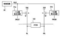
(実施の形態6)
以下、本発明の実施の形態6による半導体記憶装置について、図面を参照しながら説明する。
本実施の形態6による半導体記憶装置は、図12に示すように、プリチャージ回路の活性化信号であるプリチャージ制御信号のパルス幅を、通常動作時と、検査動作時とで可変とする機能を有するようにしたものである。
(Embodiment 6)
Hereinafter, a semiconductor memory device according to a sixth embodiment of the present invention will be described with reference to the drawings.
As shown in FIG. 12, the semiconductor memory device according to the sixth embodiment has a function of making the pulse width of a precharge control signal, which is an activation signal of the precharge circuit, variable between a normal operation and an inspection operation. It is made to have.
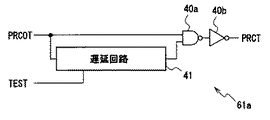
すなわち、本実施の形態6による半導体記憶装置は、図12(a)に示すように、ビット線対をプリチャージするプリチャージ回路として、各ビット線ごとに1つのプリチャージ回路を設け、具体的にはビット線BL0,XBL0,BL1,XBL1にプリチャージ回路101a,101b,101c,101dを設け、正論理側ビット線BLにつながるプリチャージ回路101a,101cと、負論理側ビット線XBLにつながるプリチャージ回路101b,101dは、制御回路60により制御される第1、第2のパルス幅発生回路61a,61bからのそれぞれ別の活性化信号PRCT、PRCBにより活性化される構成としている。
That is, the semiconductor memory device according to the sixth embodiment is provided with one precharge circuit for each bit line as a precharge circuit for precharging a bit line pair, as shown in FIG. Are provided with
また、図12(b)に示すように、正論理側ビット線BLにつながるプリチャージ回路を構成するトランジスタQ1のゲートは、パルス幅発生回路61aにて制御回路60からの制御信号TESTに応じて活性化信号PRCOTを遅延して得られる信号PRCTにより制御され、負論理側ビット線XBLにつながるプリチャージ回路を構成するトランジスタQ2のゲートは、パルス幅発生回路61bにて制御回路60からの制御信号TESTに応じて活性化信号PRCOTを遅延して得られる信号PRCBにより制御される。
As shown in FIG. 12B, the gate of the transistor Q1 constituting the precharge circuit connected to the positive logic side bit line BL is in response to the control signal TEST from the
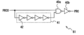
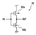
通常、パルス幅を発生する回路61は、図13(a)に示すように遅延回路41と論理回路40a及び40bで構成され、その遅延回路41は、図13(c)に示すようなインバータ42の多段接続によって構成される。このインバータ42は、Pチャネルトランジスタ42aとNチャネルトランジスタ42bとをVdd電源とVss電源との間に直列に接続してなるもので、両トランジスタの共通ゲートが入力ノード、両トランジスタの接続点が出力ノードとなっている。
Normally, the
そして、上記パルス発生回路を構成するインバータ42の一部に、図13(d)に示すように、通常動作と、検査動作を切替えるTEST信号を入力する回路を設けることにより、この入力によって、上記遅延回路41の遅延時間を可変とし、すなわちその出力パルス幅を可変とし、ひいては、その出力によってプリチャージトランジスタの駆動能力を切替える構成とすることができ、図12(a),(b)に示す本実施の形態6の第1,第2の活性化信号PRCOT,PRCOBを入力とするパルス幅発生回路61a,61bを、容易に実現することができるものである。
Then, as shown in FIG. 13 (d), by providing a circuit for inputting a TEST signal for switching between the normal operation and the inspection operation, a part of the
なお、図13(b)は、本実施の形態6の第1の活性化信号PRCOTを入力とするパルス幅発生回路61aを示しており、また、図13(d)は、上記パルス幅発生回路61aにおける遅延回路を構成する1つのインバータを示している。このインバータは、図13(c)に示すインバータ42のNチャネルトランジスタ42bと低電位側電源Vssとの間に、並列接続のPチャネルトランジスタ43a及び43bを接続してなるもので、その一方のPチャネルトランジスタ43aのゲートは高電位側電源Vddに接続され、その他方のPチャネルトランジスタ43bのゲートには制御回路60からのテスト信号TESTが入力される。
FIG. 13 (b) shows a pulse
このようにすれば、スクリーニング検査時には、制御回路60からのテスト信号TESTを、Pチャネルトランジスタ43bがオンして遅延回路41の遅延時間が短くなるよう“L”レベルとして、プリチャージパルス幅を短くすることで、ビット線が“L”レベルから“H”レベルに十分にプリチャージする前に、プリチャージ動作を完了させることができるものであり、その結果、読出し前のビット線電位差を生じさせることができ、前述のように、スクリーニングを行うことができる。
In this way, during the screening test, the test signal TEST from the
ここで、上述したように従来技術でのスクリーニング手法では、センスアンプの動作タイミングを早めることによりスクリーニングを行っているところ、最近の半導体素子の低電圧化及び高速化に伴いセンスアンプの動作タイミングはほとんどマージンの無い設計となっているため、上記従来の方法では実質的に動作タイミングを早めることはほぼ不可能であったが、一方、本実施の形態6では、アクセス速度に直接関与しないプリチャージ時間を制御しているため、SRAMの動作マージンを損ねることなく、容易にこのスクリーニングを実現できるものであり、本実施の形態6においては、このようにして上記実施の形態1と同様の効果を得ることができるものである。 Here, as described above, in the screening method in the prior art, screening is performed by accelerating the operation timing of the sense amplifier. However, the operation timing of the sense amplifier is recently increased due to the lower voltage and higher speed of the semiconductor element. Since the design has almost no margin, it is almost impossible to advance the operation timing substantially by the above-described conventional method. On the other hand, in the sixth embodiment, precharge that is not directly related to the access speed is performed. Since the time is controlled, this screening can be easily realized without impairing the operation margin of the SRAM. In the sixth embodiment, the same effect as in the first embodiment is obtained in this way. It can be obtained.
以上のような本実施の形態6による半導体集積装置によれば、SRAMを搭載した半導体記憶装置において、SRAMのビット線対の各ビット線のそれぞれにプリチャージ回路を接続し、各プリチャージ回路は同一の電源電圧に接続し、ビット線対の一方のビット線に接続した第1のプリチャージ回路は第1の遅延回路を介して第1の活性化信号で活性化し、ビット線対の他方のビット線に接続した第2のプリチャージ回路は第2の遅延回路を介して第2の活性化信号で活性化し、第1および第2の各活性化信号は互いに独立に制御されるものとし、プリチャージ回路の通常動作モードと検査動作モードとの切替えは第1および第2の遅延回路を制御する制御回路によって行い、検査時において読出し動作前に記第1および第2の活性化信号を活性化することによってビット線対の一方のビット線と前記ビット線対の他方のビット線とを互いに異なるプリチャージ電位までプリチャージする手段が構成されるものとし、さらに、上記構成において各プリチャージ回路はPチャネル型トランジスタからなり、ビット線対の一方のビット線とビット線対の他方のビット線とを互いに異なるプリチャージ電位までプリチャージする手段は、第1および第2の遅延回路により各プリチャージ回路の一方のPチャネル型トランジスタの立ち上がり動作を、各プリチャージ回路の他方のPチャネル型トランジスタの立ち上がり動作よりも早めて、各プリチャージ回路の一方のPチャネル型トランジスタのプリチャージが不十分な状態でプリチャージ動作を完了するよう制御されるようにしたので、スクリーニング検査時にはプリチャージパルス幅を短くしてビット線が“L”レベルから“H”レベルに十分にプリチャージする前にプリチャージ動作を完了させることができるようになり、その結果、十分に読出し前のビット線電位差を生じさせることができ、スクリーニングを確実に行うことができる。また、従来技術のスクリーニング手法では、最近の半導体素子の低電圧化及び高速化に伴いセンスアンプの動作タイミングはほとんどマージンの無い設計となっているため、実質的にスクリーニングのために動作タイミングを早めることはほぼ不可能であったが、本実施の形態6では、アクセス速度に直接関与しないプリチャージ時間を制御するようにしているため、SRAMの動作マージンを損ねることなく容易にこのスクリーニングを実現することができるものである。 According to the semiconductor integrated device according to the sixth embodiment as described above, in the semiconductor memory device mounting the SRAM, a precharge circuit is connected to each bit line of the SRAM bit line pair, and each precharge circuit is The first precharge circuit connected to the same power supply voltage and connected to one bit line of the bit line pair is activated by the first activation signal via the first delay circuit, and the other of the bit line pair is activated. The second precharge circuit connected to the bit line is activated by the second activation signal via the second delay circuit, and the first and second activation signals are controlled independently of each other, Switching between the normal operation mode and the inspection operation mode of the precharge circuit is performed by a control circuit that controls the first and second delay circuits, and the first and second activation signals before the read operation at the time of inspection. A means for precharging one bit line of the bit line pair and the other bit line of the bit line pair to different precharge potentials by being activated is configured. The circuit is composed of a P-channel transistor, and means for precharging one bit line of the bit line pair and the other bit line of the bit line pair to different precharge potentials is provided by the first and second delay circuits. The rise operation of one P-channel transistor of the precharge circuit is made earlier than the rise operation of the other P-channel transistor of each precharge circuit, so that the precharge of one P-channel transistor of each precharge circuit is not performed. Since it was controlled to complete the precharge operation in a sufficient state During the screening test, the precharge pulse width is shortened so that the precharge operation can be completed before the bit line is sufficiently precharged from the “L” level to the “H” level. The previous bit line potential difference can be generated, and screening can be performed reliably. Further, in the conventional screening method, the operation timing of the sense amplifier is designed to have almost no margin with the recent reduction in voltage and speed of the semiconductor element, so that the operation timing is substantially advanced for screening. In the sixth embodiment, since the precharge time that is not directly related to the access speed is controlled, this screening can be realized easily without deteriorating the operation margin of the SRAM. It is something that can be done.
以上説明したように、本発明の半導体記憶装置、及びその検査方法は、通常動作ではスクリーニングできない、工程不良等によるSNM値不足による信頼性不良を、初期検査でスクリーングすることができ、特に、SRAMのスクリーニング方法等に有用である。 As described above, the semiconductor memory device and the inspection method thereof according to the present invention can screen the reliability failure due to the shortage of the SNM value due to the process failure or the like in the initial inspection, which cannot be screened in the normal operation. This is useful for SRAM screening methods and the like.
PRC0 通常動作時用プリチャージ活性化信号
PRCT スクリーニング検査時用正論理ビット線プリチャージ回路活性化信号
PRCB スクリーニング検査時用負論理ビット線プリチャージ回路活性化信号
101a,101b,101c,101d 通常動作時用プリチャージ回路
102a,102b,102c,102d スクリーニング検査時用プリチャージ回路
103 メモリセル
WL ワード線活性化信号
SA センスアンプ活性化信号
BL0 正論理側ビット線
XBL0 負論理側ビット線
SN 正論理側メモリセル内部ノード
XSN 負論理側メモリセル内部ノード
Q1、Q2、Q3、Q4 プリチャージ用トランジスタ
PRC0 Normal operation precharge activation signal PRCT Screening inspection positive logic bit line precharge circuit activation signal PRCB Screening inspection negative logic bit line precharge
Claims (17)
前記SRAMのビット線対の一方のビット線に第1の通常動作用プリチャージ回路および第1の検査用プリチャージ回路の各一端が並列接続されており、
前記SRAMのビット線対の他方のビット線に第2の通常動作用プリチャージ回路および第2の検査用プリチャージ回路の各一端が並列接続されており、
前記第1および第2の通常動作用プリチャージ回路および第1および第2の検査用プリチャージ回路は同一の電源電圧に接続されており、
前記ビット線対の一方および他方のビット線のそれぞれに接続された第1および第2の通常動作用プリチャージ回路は共に第1の活性化信号で活性化され、
前記ビット線対の一方のビット線に接続された第1の検査用プリチャージ回路は第2の活性化信号で活性化され、
前記ビット線対の他方のビット線に接続された第2の検査用プリチャージ回路は第3の活性化信号で活性化され、
前記第1ないし第3の活性化信号は互いに独立に制御され、
該半導体記憶装置の検査時において読出し動作前に、前記ビット線対の他方のビット線が第1のプリチャージ電位にある状態で、前記第2の活性化信号を活性化することにより、前記ビット線対の一方のビット線を第2のプリチャージ電位にして、または前記ビット線対の一方のビット線が第1のプリチャージ電位にある状態で、前記第3の活性化信号を活性化することにより、前記ビット線対の他方のビット線を第2のプリチャージ電位にして、前記ビット線対の一方のビット線と前記ビット線対の他方のビット線とを互いに異なるプリチャージ電位までプリチャージするプリチャージ手段を、備えた、
ことを特徴とする半導体記憶装置。 A semiconductor memory device equipped with SRAM,
One end of each of the first normal operation precharge circuit and the first inspection precharge circuit is connected in parallel to one bit line of the SRAM bit line pair,
Each one end of the second normal operation precharge circuit and the second inspection precharge circuit is connected in parallel to the other bit line of the SRAM bit line pair,
The first and second normal operation precharge circuits and the first and second test precharge circuits are connected to the same power supply voltage;
Both the first and second normal operation precharge circuits connected to one and the other bit lines of the bit line pair are activated by a first activation signal,
The first inspection precharge circuit connected to one bit line of the bit line pair is activated by a second activation signal;
A second test precharge circuit connected to the other bit line of the bit line pair is activated by a third activation signal;
The first to third activation signals are controlled independently of each other;
By activating the second activation signal while the other bit line of the bit line pair is at the first precharge potential before the read operation at the time of inspection of the semiconductor memory device, the bit The third activation signal is activated in a state where one bit line of the line pair is set to the second precharge potential or one bit line of the bit line pair is at the first precharge potential. As a result, the other bit line of the bit line pair is set to the second precharge potential, and one bit line of the bit line pair and the other bit line of the bit line pair are precharged to different precharge potentials. Provided with pre-charging means for charging,
A semiconductor memory device.
前記ビット線対の各ビット線の電位を設定するセンスアンプは、
該半導体記憶装置の検査時において読出し動作前に、メモリセルに保持されているデータに応じて、前記ビット線対の一方のビット線をHまたはLレベルの所定の論理電位に設定し、その他方のビット線を、該一方のビット線に設定される論理電位とは相補型の論理電位に設定し、
前記プリチャージ手段は、前記センスアンプにより前記ビット線対の他方のビット線が前記第1のプリチャージ電位と等しいHレベル論理電位に設定されているとき、前記第2の活性化信号を活性化して、Lレベル論理電位に設定されている一方のビット線を、前記Hレベル論理電位より低い第2のプリチャージ電位に充電し、前記センスアンプにより前記一方のビット線が前記第1のプリチャージ電位と等しいHレベル論理電位に設定されているとき、前記第3の活性化信号を活性化して、Lレベル論理電位に設定されている他方のビット線を、前記Hレベル論理電位より低い第2のプリチャージ電位に充電する、
ことを特徴とする半導体記憶装置。 The semiconductor memory device according to claim 1,
The sense amplifier that sets the potential of each bit line of the bit line pair is:
One bit line of the bit line pair is set to a predetermined logic potential of H or L level according to the data held in the memory cell before the read operation at the time of inspection of the semiconductor memory device. Is set to a logic potential complementary to the logic potential set to the one bit line,
The precharge means activates the second activation signal when the other bit line of the bit line pair is set to an H level logic potential equal to the first precharge potential by the sense amplifier. One bit line set to the L level logic potential is charged to a second precharge potential lower than the H level logic potential, and the one bit line is set to the first precharge by the sense amplifier. When the H level logic potential equal to the potential is set, the third activation signal is activated, and the other bit line set to the L level logic potential is set to the second level lower than the H level logic potential. To the precharge potential of
A semiconductor memory device.
前記第1および第2の通常動作用プリチャージ回路および前記第1および第2の検査用プリチャージ回路は共にPチャネル型トランジスタからなり、
前記プリチャージ手段は、前記第1および第2の検査用プリチャージ回路のPチャネル型トランジスタが前記第1および第2の通常動作用プリチャージ回路のPチャネル型トランジスタより駆動能力が小さいトランジスタよりなる、
ことを特徴とする半導体記憶装置。 The semiconductor memory device according to claim 1,
The first and second normal operation precharge circuits and the first and second test precharge circuits are both P-channel transistors,
The precharge means comprises a transistor in which the P channel type transistors of the first and second test precharge circuits have a smaller driving capability than the P channel type transistors of the first and second normal operation precharge circuits. ,
A semiconductor memory device.
前記第1および第2の通常動作用プリチャージ回路はPチャネル型トランジスタからなり、
前記第1および第2の検査用プリチャージ回路はNチャネル型トランジスタからなり、
前記プリチャージ手段は、前記第1および第2の通常動作用プリチャージ回路が接続されたビット線に第1のプリチャージ電位を印加し、前記第1および第2の検査用プリチャージ回路が接続されたビット線に前記第1のプリチャージ電位よりも前記Nチャネル型トランジスタの閾値電圧分低い第2のプリチャージ電位を印加してプリチャージを行う、
ことを特徴とする半導体記憶装置。 The semiconductor memory device according to claim 1,
The first and second normal operation precharge circuits comprise P-channel transistors,
The first and second test precharge circuits comprise N-channel transistors,
The precharge means applies a first precharge potential to the bit line to which the first and second normal operation precharge circuits are connected, and the first and second test precharge circuits are connected. Precharging is performed by applying a second precharge potential lower than the first precharge potential by the threshold voltage of the N-channel transistor to the bit line formed,
A semiconductor memory device.
前記SRAMのビット線対の一方のビット線に第1の通常動作用プリチャージ回路および第1の検査用プリチャージ回路の各一端が並列接続されており、
前記SRAMのビット線対の他方のビット線に第2の通常動作用プリチャージ回路および第2の検査用プリチャージ回路の各一端が並列接続されており、
前記第1および第2の通常動作用プリチャージ回路は第1の電源電圧に接続されており、
前記第1および第2の検査用プリチャージ回路は前記第1の電源電圧よりも低い第2の電源電圧に接続されており、
前記ビット線対の一方のビット線に接続された第1の通常動作用プリチャージ回路は第1の活性化信号で活性化され、
前記ビット線対の他方のビット線に接続された第2の通常動作用プリチャージ回路は第2の活性化信号で活性化され、
前記ビット線対の一方のビット線に接続された第1の検査用プリチャージ回路は第3の活性化信号で活性化され、
前記ビット線対の他方のビット線に接続された第2の検査用プリチャージ回路は第4の活性化信号で活性化され、
前記第1乃至第4の各活性化信号は互いに独立に制御され、
該半導体記憶装置の検査時において読出し動作前に、前記第1および第4の活性化信号を活性化するか、または前記第2および第3の活性化信号を活性化することにより、前記ビット線対の一方のビット線と前記ビット線対の他方のビット線とを互いに異なるプリチャージ電位までプリチャージするプリチャージ手段を、備えた、
ことを特徴とする半導体記憶装置。 A semiconductor memory device equipped with SRAM,
One end of each of the first normal operation precharge circuit and the first inspection precharge circuit is connected in parallel to one bit line of the SRAM bit line pair,
Each one end of the second normal operation precharge circuit and the second inspection precharge circuit is connected in parallel to the other bit line of the SRAM bit line pair,
The first and second normal operation precharge circuits are connected to a first power supply voltage;
The first and second test precharge circuits are connected to a second power supply voltage lower than the first power supply voltage;
A first normal operation precharge circuit connected to one bit line of the bit line pair is activated by a first activation signal;
A second normal operation precharge circuit connected to the other bit line of the bit line pair is activated by a second activation signal;
The first inspection precharge circuit connected to one bit line of the bit line pair is activated by a third activation signal;
A second test precharge circuit connected to the other bit line of the bit line pair is activated by a fourth activation signal;
The first to fourth activation signals are controlled independently of each other,
The bit line is activated by activating the first and fourth activation signals or activating the second and third activation signals before a read operation at the time of testing the semiconductor memory device. Precharge means for precharging one bit line of the pair and the other bit line of the bit line pair to different precharge potentials;
A semiconductor memory device.
前記第1および第2の通常動作用プリチャージ回路および前記第1および第2の検査用プリチャージ回路は共にPチャネル型トランジスタからなり、
前記プリチャージ手段は、前記第1および第2の検査用プリチャージ回路のPチャネル型トランジスタと前記第1および第2の通常動作用プリチャージ回路のPチャネル型トランジスタとが駆動能力が等しいトランジスタよりなる、
ことを特徴とする半導体記憶装置。 The semiconductor memory device according to claim 5.
The first and second normal operation precharge circuits and the first and second test precharge circuits are both P-channel transistors,
The precharge means includes a transistor in which the P channel type transistors of the first and second test precharge circuits and the P channel type transistors of the first and second normal operation precharge circuits have the same driving capability. Become,
A semiconductor memory device.
前記SRAMのビット線対の一方のビット線に第1の通常動作用プリチャージ回路および第1の検査用プリチャージ回路の各一端が並列接続されており、
前記SRAMのビット線対の他方のビット線に第2の通常動作用プリチャージ回路および第2の検査用プリチャージ回路の各一端が並列接続されており、
前記第1および第2の通常動作用プリチャージ回路および第1および第2の検査用プリチャージ回路は同一の電源電圧に接続されており、
前記ビット線対の一方のビット線に接続された第1の通常動作用プリチャージ回路は第1の活性化信号で活性化され、
前記ビット線対の他方のビット線に接続された第2の通常動作用プリチャージ回路は第2の活性化信号で活性化され、
前記ビット線対の一方のビット線に接続された第1の検査用プリチャージ回路は第1のレベルシフト回路を介して第3の活性化信号で活性化され、
前記ビット線対の他方のビット線に接続された第2の検査用プリチャージ回路は第2のレベルシフト回路を介して第4の活性化信号で活性化され、
前記第1乃至第4の各活性化信号は互いに独立に制御され、
該半導体記憶装置の検査時において読出し動作前に、前記第1および第4の活性化信号を活性化するか、または前記第2および第3の活性化信号を活性化することにより、前記ビット線対の一方のビット線と前記ビット線対の他方のビット線とを互いに異なるプリチャージ電位までプリチャージするプリチャージ手段を、備えた、
ことを特徴とする半導体記憶装置。 A semiconductor memory device equipped with SRAM,
One end of each of the first normal operation precharge circuit and the first inspection precharge circuit is connected in parallel to one bit line of the SRAM bit line pair,
Each one end of the second normal operation precharge circuit and the second inspection precharge circuit is connected in parallel to the other bit line of the SRAM bit line pair,
The first and second normal operation precharge circuits and the first and second test precharge circuits are connected to the same power supply voltage;
A first normal operation precharge circuit connected to one bit line of the bit line pair is activated by a first activation signal;
A second normal operation precharge circuit connected to the other bit line of the bit line pair is activated by a second activation signal;
The first inspection precharge circuit connected to one bit line of the bit line pair is activated by a third activation signal via the first level shift circuit,
The second inspection precharge circuit connected to the other bit line of the bit line pair is activated by a fourth activation signal via the second level shift circuit,
The first to fourth activation signals are controlled independently of each other,
The bit line is activated by activating the first and fourth activation signals or activating the second and third activation signals before a read operation at the time of testing the semiconductor memory device. Precharge means for precharging one bit line of the pair and the other bit line of the bit line pair to different precharge potentials;
A semiconductor memory device.
前記第1および第2の通常動作用プリチャージ回路および第1および第2の検査用プリチャージ回路は共にPチャネル型トランジスタからなり、
前記プリチャージ手段は、前記第1および第2のレベルシフト回路により前記第1および第2の検査用プリチャージ回路のPチャネル型トランジスタの駆動能力が前記第1および第2の通常動作用プリチャージ回路のPチャネル型トランジスタの駆動能力より小さくなるよう制御する、
ことを特徴とする半導体記憶装置。 The semiconductor memory device according to claim 7,
The first and second normal operation precharge circuits and the first and second test precharge circuits are both P-channel transistors,
In the precharge means, the first and second level shift circuits allow the first and second inspection precharge circuits to drive the P-channel transistors in the first and second normal operation precharges. Control to be smaller than the driving capability of the P-channel transistor of the circuit,
A semiconductor memory device.
前記SRAMのビット線対の一方および他方のビット線のそれぞれに第1および第2のプリチャージ回路が接続されており、
前記第1および第2のプリチャージ回路は同一の電源電圧に接続されており、
前記ビット線対の一方のビット線に接続された第1のプリチャージ回路は第1のレベルシフト回路を介して第1の活性化信号で活性化され、
前記ビット線対の他方のビット線に接続された第2のプリチャージ回路は第2のレベルシフト回路を介して第2の活性化信号で活性化され、
前記第1および第2の活性化信号は互いに独立に制御され、
前記第1および第2のプリチャージ回路の通常動作モードと検査動作モードとの切替えは前記第1および第2のレベルシフト回路を制御する制御回路によって行なわれ、
該半導体記憶装置の検査時において読出し動作前に、前記第1および第2の活性化信号を活性化することにより、前記ビット線対の一方のビット線と他方のビット線とを互いに異なるプリチャージ電位までプリチャージするプリチャージ手段を、備えた、
ことを特徴とする半導体記憶装置。 A semiconductor memory device equipped with SRAM,
First and second precharge circuits are connected to one and the other bit lines of the SRAM bit line pair,
The first and second precharge circuits are connected to the same power supply voltage,
A first precharge circuit connected to one bit line of the bit line pair is activated by a first activation signal via a first level shift circuit;
A second precharge circuit connected to the other bit line of the bit line pair is activated by a second activation signal via a second level shift circuit;
The first and second activation signals are controlled independently of each other;
Switching between the normal operation mode and the test operation mode of the first and second precharge circuits is performed by a control circuit that controls the first and second level shift circuits,
By activating the first and second activation signals before the read operation at the time of testing the semiconductor memory device, one bit line and the other bit line of the bit line pair are precharged differently from each other. Provided with a precharge means for precharging to a potential;
A semiconductor memory device.
前記第1および第2のプリチャージ回路はPチャネル型トランジスタからなり、
前記プリチャージ手段は、前記第1および第2のレベルシフト回路により前記第1および第2のプリチャージ回路の一方のPチャネル型トランジスタの駆動能力が前記第1および第2のプリチャージ回路の他方のPチャネル型トランジスタの駆動能力より小さくなるよう制御する、
ことを特徴とする半導体記憶装置。 The semiconductor memory device according to claim 9.
The first and second precharge circuits comprise P-channel transistors,
In the precharge means, the first and second level shift circuits cause the drive capability of one P-channel transistor of the first and second precharge circuits to be the other of the first and second precharge circuits. Control to be smaller than the driving capability of the P-channel transistor of
A semiconductor memory device.
前記SRAMのビット線対の一方および他方のビット線のそれぞれに第1および第2のプリチャージ回路が接続されており、
前記第1および第2のプリチャージ回路は同一の電源電圧に接続されており、
前記ビット線対の一方のビット線に接続された第1のプリチャージ回路は第1の遅延回路を介して第1の活性化信号で活性化され、
前記ビット線対の他方のビット線に接続された第2のプリチャージ回路は第2の遅延回路を介して第2の活性化信号で活性化され、
前記第1および第2の各活性化信号は互いに独立に制御され、
前記第1および第2のプリチャージ回路の通常動作モードと検査動作モードとの切替えは、前記第1および第2の遅延回路を制御する制御回路によって行なわれ、
該半導体装置の検査時において読出し動作前に、前記第1および第2の活性化信号を活性化することにより、前記ビット線対の一方のビット線と他方のビット線とを互いに異なるプリチャージ電位までプリチャージするプリチャージ手段を、備えた、
ことを特徴とする半導体記憶装置。 A semiconductor memory device equipped with SRAM,
First and second precharge circuits are connected to one and the other bit lines of the SRAM bit line pair,
The first and second precharge circuits are connected to the same power supply voltage,
A first precharge circuit connected to one bit line of the bit line pair is activated by a first activation signal via a first delay circuit;
A second precharge circuit connected to the other bit line of the bit line pair is activated by a second activation signal via a second delay circuit;
The first and second activation signals are controlled independently of each other,
Switching between the normal operation mode and the inspection operation mode of the first and second precharge circuits is performed by a control circuit that controls the first and second delay circuits,
By activating the first and second activation signals before the read operation during the inspection of the semiconductor device, one bit line and the other bit line of the bit line pair are made to have different precharge potentials. Equipped with precharge means for precharging up to,
A semiconductor memory device.
前記第1および第2のプリチャージ回路はPチャネル型トランジスタからなり、
前記プリチャージ手段は、前記第1および第2の遅延回路により前記第1および第2のプリチャージ回路の一方のPチャネル型トランジスタの立ち上がり動作を前記第1および第2のプリチャージ回路の他方のPチャネル型トランジスタの立ち上がり動作より早めて、前記第1および第2のプリチャージ回路の一方のPチャネル型トランジスタのプリチャージが不十分な状態でプリチャージ動作を完了させる、
ことを特徴とする半導体記憶装置。 The semiconductor memory device according to claim 11,
The first and second precharge circuits comprise P-channel transistors,
The precharge means performs a rising operation of one P-channel transistor of the first and second precharge circuits with the other of the first and second precharge circuits by the first and second delay circuits. A precharge operation is completed in a state where the precharge of one P channel transistor of the first and second precharge circuits is insufficient before the rising operation of the P channel transistor.
A semiconductor memory device.
前記第1または第2の通常動作用プリチャージ回路が接続された前記ビット線対の一方のビット線に第1のプリチャージ電位を印加し、前記第1または第2の検査用プリチャージ回路が接続された前記ビット線対の他方のビット線に前記第1のプリチャージ電位より低い第2のプリチャージ電位を印加する第1の工程と、
前記第1の工程の後に読出し動作を行なって動作マージン検査を行う第2の工程と、を有する、
ことを特徴とする半導体記憶装置の検査方法。 A method for inspecting a semiconductor memory device according to claim 1, comprising:
A first precharge potential is applied to one bit line of the bit line pair to which the first or second normal operation precharge circuit is connected, and the first or second test precharge circuit is Applying a second precharge potential lower than the first precharge potential to the other bit line of the connected bit line pair;
A second step of performing an operation margin inspection by performing a read operation after the first step;
A method of inspecting a semiconductor memory device.
前記第1または第2の通常動作用プリチャージ回路が接続された前記ビット線対の一方のビット線に第1の電源電圧を印加し、前記第1または第2の検査用プリチャージ回路が接続された前記ビット線対の他方のビット線に前記第2の電源電圧を印加する第1の工程と、
前記第1の工程の後に読出し動作を行なって動作マージン検査を行う第2の工程と、を有する、
ことを特徴とする半導体記憶装置の検査方法。 A method for inspecting a semiconductor memory device according to claim 5, comprising:
A first power supply voltage is applied to one bit line of the bit line pair to which the first or second normal operation precharge circuit is connected, and the first or second test precharge circuit is connected. A first step of applying the second power supply voltage to the other bit line of the paired bit lines;
A second step of performing an operation margin inspection by performing a read operation after the first step;
A method of inspecting a semiconductor memory device.
前記第1または第2の通常動作用プリチャージ回路が接続された前記ビット線対の一方のビット線に電源電圧を印加し、前記第1または第2の検査用プリチャージ回路が接続された前記ビット線対の他方のビット線に前記第1または第2のレベルシフト回路によって前記電源電圧よりも低く設定された電位を印加する第1の工程と、
前記第1の工程の後に読出し動作を行なって動作マージン検査を行う第2の工程と、を有する、
ことを特徴とする半導体記憶装置の検査方法。 8. A method for inspecting a semiconductor memory device according to claim 7, comprising:
A power supply voltage is applied to one bit line of the bit line pair to which the first or second normal operation precharge circuit is connected, and the first or second test precharge circuit is connected. A first step of applying a potential set lower than the power supply voltage by the first or second level shift circuit to the other bit line of the bit line pair;
A second step of performing an operation margin inspection by performing a read operation after the first step;
A method of inspecting a semiconductor memory device.
前記第2のプリチャージ回路が接続された前記ビット線対の他方のビット線に電源電圧を印加し、前記第1のプリチャージ回路が接続された前記ビット線対の一方のビット線に前記第1および第2のレベルシフト回路によって前記電源電圧よりも低く設定された電位を印加する第1の工程と、
前記第1の工程の後に読出し動作を行なって動作マージン検査を行う第2の工程と、を有する、
ことを特徴とする半導体記憶装置の検査方法。 A method for inspecting a semiconductor memory device according to claim 9, comprising:
A power supply voltage is applied to the other bit line of the bit line pair connected to the second precharge circuit, and the first bit line of the bit line pair connected to the first precharge circuit is applied to the first bit line. A first step of applying a potential set lower than the power supply voltage by the first and second level shift circuits;
A second step of performing an operation margin inspection by performing a read operation after the first step;
A method of inspecting a semiconductor memory device.
前記第2のプリチャージ回路を第2の遅延回路を介して第2の活性化信号により活性化して、前記第2のプリチャージ回路が接続された前記ビット線対の他方のビット線に電源電圧を印加し、前記第1のプリチャージ回路を第1の遅延回路を介して第1の活性化信号により活性化し、前記第1のプリチャージ回路の立ち上がり動作を前記第1の遅延回路によって前記第2のプリチャージ回路の立ち上がり動作よりも早めて、プリチャージが不十分な状態で該プリチャージ動作を完了して、前記第1のプリチャージ回路が接続された前記ビット線対の一方のビット線に、前記電源電圧よりも低い電位を印加する第1の工程と、
前記第1の工程の後に読出し動作を行なって動作マージン検査を行う第2の工程と、を有する、
ことを特徴とする半導体記憶装置の検査方法。 12. A method of inspecting a semiconductor memory device according to claim 11, comprising:
The second precharge circuit is activated by a second activation signal through a second delay circuit, and a power supply voltage is applied to the other bit line of the bit line pair to which the second precharge circuit is connected. , The first precharge circuit is activated by the first activation signal via the first delay circuit, and the rising operation of the first precharge circuit is activated by the first delay circuit. The bit line pair of the bit line pair to which the first precharge circuit is connected is completed earlier than the rise operation of the precharge circuit 2 and the precharge operation is completed in a state where the precharge is insufficient. And a first step of applying a potential lower than the power supply voltage;
A second step of performing an operation margin inspection by performing a read operation after the first step;
A method of inspecting a semiconductor memory device.
Priority Applications (1)
| Application Number | Priority Date | Filing Date | Title |
|---|---|---|---|
| JP2005290283A JP2007102902A (en) | 2005-10-03 | 2005-10-03 | Semiconductor memory device and inspection method thereof |
Applications Claiming Priority (1)
| Application Number | Priority Date | Filing Date | Title |
|---|---|---|---|
| JP2005290283A JP2007102902A (en) | 2005-10-03 | 2005-10-03 | Semiconductor memory device and inspection method thereof |
Publications (1)
| Publication Number | Publication Date |
|---|---|
| JP2007102902A true JP2007102902A (en) | 2007-04-19 |
Family
ID=38029680
Family Applications (1)
| Application Number | Title | Priority Date | Filing Date |
|---|---|---|---|
| JP2005290283A Pending JP2007102902A (en) | 2005-10-03 | 2005-10-03 | Semiconductor memory device and inspection method thereof |
Country Status (1)
| Country | Link |
|---|---|
| JP (1) | JP2007102902A (en) |
Cited By (7)
| Publication number | Priority date | Publication date | Assignee | Title |
|---|---|---|---|---|
| DE102008017813A1 (en) | 2007-04-10 | 2008-10-23 | Toyota Jidosha Kabushiki Kaisha, Toyota-shi | Brake control device and brake control method |
| JP2009117026A (en) * | 2007-11-05 | 2009-05-28 | Sony Computer Entertainment Inc | Bit line screening method of sram |
| JP2010027155A (en) * | 2008-07-22 | 2010-02-04 | Sanyo Electric Co Ltd | Semiconductor memory device |
| JP2010061731A (en) * | 2008-09-03 | 2010-03-18 | Nec Electronics Corp | Sram (static random access memory) and sram test method |
| JP2011204295A (en) * | 2010-03-24 | 2011-10-13 | Renesas Electronics Corp | Semiconductor memory and load test method thereof |
| US8284591B2 (en) | 2009-02-27 | 2012-10-09 | Renesas Electronics Corporation | Semiconductor memory device and test method therefor |
| JP2016085775A (en) * | 2014-10-27 | 2016-05-19 | ルネサスエレクトロニクス株式会社 | Semiconductor device |
-
2005
- 2005-10-03 JP JP2005290283A patent/JP2007102902A/en active Pending
Cited By (8)
| Publication number | Priority date | Publication date | Assignee | Title |
|---|---|---|---|---|
| DE102008017813A1 (en) | 2007-04-10 | 2008-10-23 | Toyota Jidosha Kabushiki Kaisha, Toyota-shi | Brake control device and brake control method |
| JP2009117026A (en) * | 2007-11-05 | 2009-05-28 | Sony Computer Entertainment Inc | Bit line screening method of sram |
| JP2010027155A (en) * | 2008-07-22 | 2010-02-04 | Sanyo Electric Co Ltd | Semiconductor memory device |
| JP2010061731A (en) * | 2008-09-03 | 2010-03-18 | Nec Electronics Corp | Sram (static random access memory) and sram test method |
| US8284591B2 (en) | 2009-02-27 | 2012-10-09 | Renesas Electronics Corporation | Semiconductor memory device and test method therefor |
| US8737118B2 (en) | 2009-02-27 | 2014-05-27 | Renesas Electronics Corporation | Semiconductor memory device and test method therefor |
| JP2011204295A (en) * | 2010-03-24 | 2011-10-13 | Renesas Electronics Corp | Semiconductor memory and load test method thereof |
| JP2016085775A (en) * | 2014-10-27 | 2016-05-19 | ルネサスエレクトロニクス株式会社 | Semiconductor device |
Similar Documents
| Publication | Publication Date | Title |
|---|---|---|
| EP0543408B1 (en) | Semiconductor memory and screening test method thereof | |
| KR100334184B1 (en) | Method and Apparatus for Testing a Static RAM | |
| US5185722A (en) | Semiconductor memory device having a memory test circuit | |
| KR101061080B1 (en) | SRM Cell and Array Test Apparatus and Method | |
| EP2518727A1 (en) | Differential sense amplifier without dedicated precharge transistors | |
| JPH0969300A (en) | Semiconductor memory device | |
| US6829183B2 (en) | Active restore weak write test mode | |
| CN101065809B (en) | Sram test method and SRAM test arrangement to detect weak cells | |
| JP5032004B2 (en) | Semiconductor device, semiconductor memory and reading method thereof | |
| JP2008027544A (en) | Semiconductor memory device and test method thereof | |
| JP2009070474A (en) | Semiconductor integrated circuit | |
| KR100248645B1 (en) | Semiconductor memory device and test method therefor | |
| JP2007102902A (en) | Semiconductor memory device and inspection method thereof | |
| JP5587141B2 (en) | Semiconductor device | |
| US6385103B1 (en) | Semiconductor memory device having a circuit for testing memories | |
| JP2006331511A (en) | Semiconductor memory device and inspection method thereof | |
| CN108010552B (en) | Semiconductor memory device with a plurality of memory cells | |
| JP5623688B2 (en) | Semiconductor memory device and defective cell test method | |
| US8737118B2 (en) | Semiconductor memory device and test method therefor | |
| US7787318B2 (en) | Semiconductor memory device having read operation testing function | |
| US7505339B2 (en) | Static semiconductor memory device allowing simultaneous writing of data into a plurality of memory cells | |
| JP2014099225A (en) | Semiconductor device | |
| US7286426B2 (en) | Semiconductor memory device | |
| JP4771610B2 (en) | Memory circuit and test method thereof | |
| JP2020123411A (en) | Semiconductor memory device and operating method thereof |