JP2007123330A - 半導体装置の製造方法 - Google Patents
半導体装置の製造方法 Download PDFInfo
- Publication number
- JP2007123330A JP2007123330A JP2005309769A JP2005309769A JP2007123330A JP 2007123330 A JP2007123330 A JP 2007123330A JP 2005309769 A JP2005309769 A JP 2005309769A JP 2005309769 A JP2005309769 A JP 2005309769A JP 2007123330 A JP2007123330 A JP 2007123330A
- Authority
- JP
- Japan
- Prior art keywords
- solution
- sulfuric acid
- semiconductor substrate
- hydrogen peroxide
- spm
- Prior art date
- Legal status (The legal status is an assumption and is not a legal conclusion. Google has not performed a legal analysis and makes no representation as to the accuracy of the status listed.)
- Pending
Links
Images




Classifications
-
- H—ELECTRICITY
- H10—SEMICONDUCTOR DEVICES; ELECTRIC SOLID-STATE DEVICES NOT OTHERWISE PROVIDED FOR
- H10P—GENERIC PROCESSES OR APPARATUS FOR THE MANUFACTURE OR TREATMENT OF DEVICES COVERED BY CLASS H10
- H10P50/00—Etching of wafers, substrates or parts of devices
- H10P50/20—Dry etching; Plasma etching; Reactive-ion etching
- H10P50/28—Dry etching; Plasma etching; Reactive-ion etching of insulating materials
- H10P50/282—Dry etching; Plasma etching; Reactive-ion etching of insulating materials of inorganic materials
- H10P50/283—Dry etching; Plasma etching; Reactive-ion etching of insulating materials of inorganic materials by chemical means
-
- G—PHYSICS
- G03—PHOTOGRAPHY; CINEMATOGRAPHY; ANALOGOUS TECHNIQUES USING WAVES OTHER THAN OPTICAL WAVES; ELECTROGRAPHY; HOLOGRAPHY
- G03F—PHOTOMECHANICAL PRODUCTION OF TEXTURED OR PATTERNED SURFACES, e.g. FOR PRINTING, FOR PROCESSING OF SEMICONDUCTOR DEVICES; MATERIALS THEREFOR; ORIGINALS THEREFOR; APPARATUS SPECIALLY ADAPTED THEREFOR
- G03F7/00—Photomechanical, e.g. photolithographic, production of textured or patterned surfaces, e.g. printing surfaces; Materials therefor, e.g. comprising photoresists; Apparatus specially adapted therefor
- G03F7/26—Processing photosensitive materials; Apparatus therefor
- G03F7/42—Stripping or agents therefor
- G03F7/422—Stripping or agents therefor using liquids only
- G03F7/423—Stripping or agents therefor using liquids only containing mineral acids or salts thereof, containing mineral oxidizing substances, e.g. peroxy compounds
-
- H—ELECTRICITY
- H10—SEMICONDUCTOR DEVICES; ELECTRIC SOLID-STATE DEVICES NOT OTHERWISE PROVIDED FOR
- H10D—INORGANIC ELECTRIC SEMICONDUCTOR DEVICES
- H10D84/00—Integrated devices formed in or on semiconductor substrates that comprise only semiconducting layers, e.g. on Si wafers or on GaAs-on-Si wafers
- H10D84/01—Manufacture or treatment
- H10D84/0123—Integrating together multiple components covered by H10D12/00 or H10D30/00, e.g. integrating multiple IGBTs
- H10D84/0126—Integrating together multiple components covered by H10D12/00 or H10D30/00, e.g. integrating multiple IGBTs the components including insulated gates, e.g. IGFETs
- H10D84/0165—Integrating together multiple components covered by H10D12/00 or H10D30/00, e.g. integrating multiple IGBTs the components including insulated gates, e.g. IGFETs the components including complementary IGFETs, e.g. CMOS devices
- H10D84/0167—Manufacturing their channels
-
- H—ELECTRICITY
- H10—SEMICONDUCTOR DEVICES; ELECTRIC SOLID-STATE DEVICES NOT OTHERWISE PROVIDED FOR
- H10D—INORGANIC ELECTRIC SEMICONDUCTOR DEVICES
- H10D84/00—Integrated devices formed in or on semiconductor substrates that comprise only semiconducting layers, e.g. on Si wafers or on GaAs-on-Si wafers
- H10D84/01—Manufacture or treatment
- H10D84/0123—Integrating together multiple components covered by H10D12/00 or H10D30/00, e.g. integrating multiple IGBTs
- H10D84/0126—Integrating together multiple components covered by H10D12/00 or H10D30/00, e.g. integrating multiple IGBTs the components including insulated gates, e.g. IGFETs
- H10D84/0165—Integrating together multiple components covered by H10D12/00 or H10D30/00, e.g. integrating multiple IGBTs the components including insulated gates, e.g. IGFETs the components including complementary IGFETs, e.g. CMOS devices
- H10D84/017—Manufacturing their source or drain regions, e.g. silicided source or drain regions
-
- H—ELECTRICITY
- H10—SEMICONDUCTOR DEVICES; ELECTRIC SOLID-STATE DEVICES NOT OTHERWISE PROVIDED FOR
- H10D—INORGANIC ELECTRIC SEMICONDUCTOR DEVICES
- H10D84/00—Integrated devices formed in or on semiconductor substrates that comprise only semiconducting layers, e.g. on Si wafers or on GaAs-on-Si wafers
- H10D84/01—Manufacture or treatment
- H10D84/0123—Integrating together multiple components covered by H10D12/00 or H10D30/00, e.g. integrating multiple IGBTs
- H10D84/0126—Integrating together multiple components covered by H10D12/00 or H10D30/00, e.g. integrating multiple IGBTs the components including insulated gates, e.g. IGFETs
- H10D84/0165—Integrating together multiple components covered by H10D12/00 or H10D30/00, e.g. integrating multiple IGBTs the components including insulated gates, e.g. IGFETs the components including complementary IGFETs, e.g. CMOS devices
- H10D84/0184—Manufacturing their gate sidewall spacers
-
- H—ELECTRICITY
- H10—SEMICONDUCTOR DEVICES; ELECTRIC SOLID-STATE DEVICES NOT OTHERWISE PROVIDED FOR
- H10D—INORGANIC ELECTRIC SEMICONDUCTOR DEVICES
- H10D84/00—Integrated devices formed in or on semiconductor substrates that comprise only semiconducting layers, e.g. on Si wafers or on GaAs-on-Si wafers
- H10D84/01—Manufacture or treatment
- H10D84/02—Manufacture or treatment characterised by using material-based technologies
- H10D84/03—Manufacture or treatment characterised by using material-based technologies using Group IV technology, e.g. silicon technology or silicon-carbide [SiC] technology
- H10D84/038—Manufacture or treatment characterised by using material-based technologies using Group IV technology, e.g. silicon technology or silicon-carbide [SiC] technology using silicon technology, e.g. SiGe
-
- H—ELECTRICITY
- H10—SEMICONDUCTOR DEVICES; ELECTRIC SOLID-STATE DEVICES NOT OTHERWISE PROVIDED FOR
- H10P—GENERIC PROCESSES OR APPARATUS FOR THE MANUFACTURE OR TREATMENT OF DEVICES COVERED BY CLASS H10
- H10P70/00—Cleaning of wafers, substrates or parts of devices
- H10P70/20—Cleaning during device manufacture
- H10P70/23—Cleaning during device manufacture during, before or after processing of insulating materials
Landscapes
- Physics & Mathematics (AREA)
- General Physics & Mathematics (AREA)
- Cleaning Or Drying Semiconductors (AREA)
- Exposure Of Semiconductors, Excluding Electron Or Ion Beam Exposure (AREA)
Abstract
【解決手段】半導体装置の製造方法は、硫酸および過酸化水素水を含む溶液を加熱し、溶液に所定量の硫酸および所定量の過酸化水素水を所定間隔で補充し、溶液の硫酸を所定の濃度以上に維持し、半導体基板を溶液に浸漬し、半導体基板を洗浄する。また、半導体装置の製造方法は、半導体基板上にレジスト膜を形成し、レジスト膜にレジストパターンを形成し、レジストパターンをマスクとして半導体基板を加工し、硫酸および過酸化水素水を含む溶液を加熱し、溶液に所定量の硫酸および所定量の過酸化水素水を所定間隔で補充し、溶液の硫酸を所定の濃度以上に維持し、半導体基板を溶液に浸漬し、レジストパターンを除去する。
【選択図】図10
Description
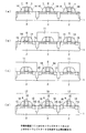
−窒化膜(以下、窒化膜とも称する)などの膜種が用いられる。そして、ゲート電極の側面にサイドウォールスペーサを形成した後、不純物をイオン注入することによりソース/ドレイン拡散領域を形成する。
以下に、SPM溶液を用いたレジスト剥離方法を説明する。まず、硫酸と過酸化水素水を混合する。次に、以下の式(1)で示すように、発熱反応により活性酸素が生成する。H2 SO4 +H2 O2 H2 SO4 +H2 O+O・・・(1)
そして、以下の式(2)で示すように、ペルオキソ一硫酸(H2 SO5 )が生成する。
H2 SO4 +H2 O2 H2 SO5 +H2 O ・・・(2)
ペルオキソ一硫酸は、以下の式(3)で示すように、H2 Oと反応することにより活性酸素を生成する。
H2 SO5 +H2 O H2 SO4 +H2 O+O・・・(3)
また、以下の式(4)で示すように、硫酸と過酸化水素水との混合によりペルオキソ二硫酸(H2 S2 O8 )が生成される。ペルオキソ二硫酸は酸化剤として作用する。
2H2 SO4 +H2 O2 →H2 S2 O8 +2H2 O ・・・・(4)
ペルオキソ二硫酸は、以下の式(5)で示すように、H2 Oと反応することにより活性酸素を生成する。
H2 S2 O8 +H2 O 2H2 SO4 +O・・・(5)
上記に示す反応により活性酸素が生成され、活性酸素等によって有機物であるレジストが分解される。また、SPM溶液を用いた洗浄により、半導体基板に付着した有機系のパーティクルと称される微粒子や金属不純物の除去も行われる。
この窒化膜のパターニングを数回繰り返した場合、窒化膜厚が減少する。窒化膜厚の減少は、窒化膜のパターニングの形成ができなくなる原因となる。
する場合、例えばボロンを用いてイオン注入を行う。
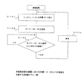
いる。内槽121に半導体基板1を浸漬させ、半導体基板1を洗浄する。内槽121に半導体基板1を浸漬させた場合、内槽121から溢れたSPM溶液を外槽122に貯める。
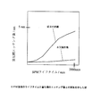
外槽122に貯まっているSPM溶液を排出する(S1104)。一方、タイマー135、136を設定してから2000分が経過していない場合は、S1103の処理を行う。S1104の処理を行った場合は、S1102の処理を再び行う。
上記のように、本実施形態の装置は、内槽121に硫酸を投入する前にSPM予備槽123で硫酸を温めている。しかし、SPM予備槽123で硫酸を温めずに内槽121に直接硫酸を投入してもよい。この場合、SPM予備槽123を設けない装置により、半導体基板1のレジスト剥離処理および洗浄処理を行う。
2 nMOS領域
3 pMOS領域
4 素子分離領域
5 ゲート絶縁膜
6 ゲート電極
7 ノッチ型サイドウォール
8 サイドウォール酸化膜
9 サイドウォール窒化膜
10 サイドウォールスペーサ
11 レジストパターン
12 ポケット領域
13 エクステンション領域
14 サイドウォール
15 ソース/ドレイン拡散領域
16 シリサイド
17 nMOSトランジスタ
18 pMOSトランジスタ
19 熱酸化膜
20 CVD−窒化膜
21 レジスト膜
22 ノッチ
120 処理槽
121 内槽
122 外槽
123 SPM予備槽
124、125、126、127、128、129 バルブ
130 廃棄バルブ
131 硫酸投入管
132 過酸化水素水投入管
133 硫酸補充管
134 過酸化水素水補充管
135、136 タイマー
137 循環パイプ
138 ポンプ
139 フィルター
140 パイプ
141 廃棄パイプ
Claims (9)
- 硫酸および過酸化水素水を含む溶液を加熱するステップと、
前記溶液に所定量の硫酸および所定量の過酸化水素水を所定間隔で補充するステップと、
前記溶液の硫酸を所定の濃度以上に維持するステップと、
半導体基板を前記溶液に浸漬し、前記半導体基板を洗浄するステップと、を有する半導体装置の製造方法。 - 前記洗浄は前記半導体基板の表面に付着している不純物を除去する請求項1に記載の半導体装置の製造方法。
- 半導体基板上にレジスト膜を形成するステップと、
前記レジスト膜にレジストパターンを形成するステップと、
前記レジストパターンをマスクとして前記半導体基板を加工するステップと、
硫酸および過酸化水素水を含む溶液を加熱するステップと、
前記溶液に所定量の硫酸および所定量の過酸化水素水を所定間隔で補充するステップと、
前記溶液の硫酸を所定の濃度以上に維持するステップと、
前記半導体基板を前記溶液に浸漬し、前記レジストパターンを除去するステップと、を有する半導体装置の製造方法。 - 前記加工は前記半導体基板にイオン注入を行う請求項3に記載の半導体装置の製造方法。
- 前記所定の濃度は75.8質量%である請求項1又は3に記載の半導体装置の製造方法。
- 前記溶液中の硫酸と過酸化水素は所定の体積比とする請求項1又は3に記載の半導体装置の製造方法。
- 前記加熱は所定の温度で行う請求項1又は3に記載の半導体装置の製造方法。
- 前記所定の体積比は4:1〜100:1である請求項6に記載の半導体装置の製造方法。
- 前記所定の温度は100℃〜140℃である請求項7に記載の半導体装置の製造方法。
Priority Applications (2)
| Application Number | Priority Date | Filing Date | Title |
|---|---|---|---|
| JP2005309769A JP2007123330A (ja) | 2005-10-25 | 2005-10-25 | 半導体装置の製造方法 |
| US11/446,304 US20070093068A1 (en) | 2005-10-25 | 2006-06-05 | Manufacturing method of semiconductor device |
Applications Claiming Priority (1)
| Application Number | Priority Date | Filing Date | Title |
|---|---|---|---|
| JP2005309769A JP2007123330A (ja) | 2005-10-25 | 2005-10-25 | 半導体装置の製造方法 |
Publications (1)
| Publication Number | Publication Date |
|---|---|
| JP2007123330A true JP2007123330A (ja) | 2007-05-17 |
Family
ID=37985925
Family Applications (1)
| Application Number | Title | Priority Date | Filing Date |
|---|---|---|---|
| JP2005309769A Pending JP2007123330A (ja) | 2005-10-25 | 2005-10-25 | 半導体装置の製造方法 |
Country Status (2)
| Country | Link |
|---|---|
| US (1) | US20070093068A1 (ja) |
| JP (1) | JP2007123330A (ja) |
Cited By (5)
| Publication number | Priority date | Publication date | Assignee | Title |
|---|---|---|---|---|
| JP2011134899A (ja) * | 2009-12-24 | 2011-07-07 | Tokyo Electron Ltd | 基板処理装置、基板処理方法及び記憶媒体 |
| JP2012049391A (ja) * | 2010-08-27 | 2012-03-08 | Kurita Water Ind Ltd | 洗浄方法および洗浄システム |
| JP2013187548A (ja) * | 2012-03-07 | 2013-09-19 | Tokyo Electron Ltd | レジストバッチ剥離プロセスのための順次段階的混合法 |
| JP2017028101A (ja) * | 2015-07-22 | 2017-02-02 | 東京エレクトロン株式会社 | 基板液処理装置、基板液処理方法及び記憶媒体 |
| WO2021220527A1 (ja) | 2020-04-28 | 2021-11-04 | 栗田工業株式会社 | 樹脂成形体のエッチング方法及び樹脂成形体用エッチング処理システム |
Families Citing this family (1)
| Publication number | Priority date | Publication date | Assignee | Title |
|---|---|---|---|---|
| JP2008058591A (ja) * | 2006-08-31 | 2008-03-13 | Toshiba Corp | 基板処理方法および電子デバイスの製造方法 |
Family Cites Families (5)
| Publication number | Priority date | Publication date | Assignee | Title |
|---|---|---|---|---|
| US7060582B2 (en) * | 2001-06-05 | 2006-06-13 | Sony Corporation | Adjusting the germanium concentration of a semiconductor layer for equal thermal expansion for a hetero-junction bipolar transistor device |
| EP1270504B1 (de) * | 2001-06-22 | 2004-05-26 | Nanoworld AG | Halbleiterbauelemente in einem Waferverbund |
| JP4040425B2 (ja) * | 2002-10-17 | 2008-01-30 | Necエレクトロニクス株式会社 | 半導体装置の製造方法 |
| JP4085384B2 (ja) * | 2003-06-09 | 2008-05-14 | ミネベア株式会社 | 薄膜パターンの形成方法 |
| JP4494840B2 (ja) * | 2003-06-27 | 2010-06-30 | 大日本スクリーン製造株式会社 | 異物除去装置、基板処理装置および基板処理方法 |
-
2005
- 2005-10-25 JP JP2005309769A patent/JP2007123330A/ja active Pending
-
2006
- 2006-06-05 US US11/446,304 patent/US20070093068A1/en not_active Abandoned
Cited By (5)
| Publication number | Priority date | Publication date | Assignee | Title |
|---|---|---|---|---|
| JP2011134899A (ja) * | 2009-12-24 | 2011-07-07 | Tokyo Electron Ltd | 基板処理装置、基板処理方法及び記憶媒体 |
| JP2012049391A (ja) * | 2010-08-27 | 2012-03-08 | Kurita Water Ind Ltd | 洗浄方法および洗浄システム |
| JP2013187548A (ja) * | 2012-03-07 | 2013-09-19 | Tokyo Electron Ltd | レジストバッチ剥離プロセスのための順次段階的混合法 |
| JP2017028101A (ja) * | 2015-07-22 | 2017-02-02 | 東京エレクトロン株式会社 | 基板液処理装置、基板液処理方法及び記憶媒体 |
| WO2021220527A1 (ja) | 2020-04-28 | 2021-11-04 | 栗田工業株式会社 | 樹脂成形体のエッチング方法及び樹脂成形体用エッチング処理システム |
Also Published As
| Publication number | Publication date |
|---|---|
| US20070093068A1 (en) | 2007-04-26 |
Similar Documents
| Publication | Publication Date | Title |
|---|---|---|
| TWI359453B (ja) | ||
| JP4393260B2 (ja) | エッチング液管理方法 | |
| US20080093343A1 (en) | Method for treating the etching solution | |
| JP2005236280A (ja) | 半導体基板用洗浄液組成物、半導体基板の洗浄方法、及び導電性構造物の製造方法 | |
| JP2001077118A (ja) | 半導体装置およびその製造方法 | |
| KR100706798B1 (ko) | 실리콘막과 실리콘 게르마늄막이 노출된 기판의 세정 방법및 이를 이용하는 반도체 제조 방법 | |
| JP5622512B2 (ja) | 半導体装置の製造方法 | |
| JP2007123330A (ja) | 半導体装置の製造方法 | |
| JP3415549B2 (ja) | 電子デバイスの洗浄方法及びその製造方法 | |
| JP5233277B2 (ja) | 半導体基板の処理方法及び半導体装置の製造方法 | |
| US6927111B2 (en) | Method for fabricating semiconductor device | |
| JP2010205782A (ja) | 半導体装置の製造方法 | |
| US7985297B2 (en) | Method of cleaning a quartz part | |
| KR100829597B1 (ko) | 반도체 장치의 세정 방법 및 제조 방법 | |
| US7727871B2 (en) | Manufacturing method of semiconductor device using etching solution | |
| JP2006093242A (ja) | 半導体装置の製造方法 | |
| JPH1050682A (ja) | 半導体装置の製造方法及び製造装置及び半導体装置 | |
| JP4108445B2 (ja) | 半導体装置の製造方法 | |
| JP2005136437A (ja) | 半導体製造システム及びクリーンルーム | |
| KR100464858B1 (ko) | 유기 스트리핑 조성물 및 이를 사용한 산화물 식각 방법 | |
| JP2002076272A (ja) | 半導体装置の製造方法 | |
| KR100933809B1 (ko) | 듀얼 게이트 산화막 형성 방법 | |
| JP2008060383A (ja) | 半導体装置の製造方法 | |
| TWI267914B (en) | Method of manufacturing semiconductor device | |
| KR100570203B1 (ko) | 게이트전극 형성방법 |
Legal Events
| Date | Code | Title | Description |
|---|---|---|---|
| A711 | Notification of change in applicant |
Free format text: JAPANESE INTERMEDIATE CODE: A712 Effective date: 20080729 |
|
| A131 | Notification of reasons for refusal |
Free format text: JAPANESE INTERMEDIATE CODE: A131 Effective date: 20090519 |
|
| A521 | Request for written amendment filed |
Free format text: JAPANESE INTERMEDIATE CODE: A523 Effective date: 20090721 |
|
| A131 | Notification of reasons for refusal |
Free format text: JAPANESE INTERMEDIATE CODE: A131 Effective date: 20090825 |
|
| A02 | Decision of refusal |
Free format text: JAPANESE INTERMEDIATE CODE: A02 Effective date: 20091222 |