JP2007123794A - Thin film transistor, pixel structure, and correction method thereof - Google Patents
Thin film transistor, pixel structure, and correction method thereof Download PDFInfo
- Publication number
- JP2007123794A JP2007123794A JP2006009125A JP2006009125A JP2007123794A JP 2007123794 A JP2007123794 A JP 2007123794A JP 2006009125 A JP2006009125 A JP 2006009125A JP 2006009125 A JP2006009125 A JP 2006009125A JP 2007123794 A JP2007123794 A JP 2007123794A
- Authority
- JP
- Japan
- Prior art keywords
- drain
- dielectric layer
- disposed
- opening
- gate pattern
- Prior art date
- Legal status (The legal status is an assumption and is not a legal conclusion. Google has not performed a legal analysis and makes no representation as to the accuracy of the status listed.)
- Pending
Links
Images


Classifications
-
- G—PHYSICS
- G02—OPTICS
- G02F—OPTICAL DEVICES OR ARRANGEMENTS FOR THE CONTROL OF LIGHT BY MODIFICATION OF THE OPTICAL PROPERTIES OF THE MEDIA OF THE ELEMENTS INVOLVED THEREIN; NON-LINEAR OPTICS; FREQUENCY-CHANGING OF LIGHT; OPTICAL LOGIC ELEMENTS; OPTICAL ANALOGUE/DIGITAL CONVERTERS
- G02F1/00—Devices or arrangements for the control of the intensity, colour, phase, polarisation or direction of light arriving from an independent light source, e.g. switching, gating or modulating; Non-linear optics
- G02F1/01—Devices or arrangements for the control of the intensity, colour, phase, polarisation or direction of light arriving from an independent light source, e.g. switching, gating or modulating; Non-linear optics for the control of the intensity, phase, polarisation or colour
- G02F1/13—Devices or arrangements for the control of the intensity, colour, phase, polarisation or direction of light arriving from an independent light source, e.g. switching, gating or modulating; Non-linear optics for the control of the intensity, phase, polarisation or colour based on liquid crystals, e.g. single liquid crystal display cells
- G02F1/133—Constructional arrangements; Operation of liquid crystal cells; Circuit arrangements
- G02F1/136—Liquid crystal cells structurally associated with a semi-conducting layer or substrate, e.g. cells forming part of an integrated circuit
- G02F1/1362—Active matrix addressed cells
-
- H—ELECTRICITY
- H10—SEMICONDUCTOR DEVICES; ELECTRIC SOLID-STATE DEVICES NOT OTHERWISE PROVIDED FOR
- H10D—INORGANIC ELECTRIC SEMICONDUCTOR DEVICES
- H10D86/00—Integrated devices formed in or on insulating or conducting substrates, e.g. formed in silicon-on-insulator [SOI] substrates or on stainless steel or glass substrates
-
- G—PHYSICS
- G02—OPTICS
- G02F—OPTICAL DEVICES OR ARRANGEMENTS FOR THE CONTROL OF LIGHT BY MODIFICATION OF THE OPTICAL PROPERTIES OF THE MEDIA OF THE ELEMENTS INVOLVED THEREIN; NON-LINEAR OPTICS; FREQUENCY-CHANGING OF LIGHT; OPTICAL LOGIC ELEMENTS; OPTICAL ANALOGUE/DIGITAL CONVERTERS
- G02F1/00—Devices or arrangements for the control of the intensity, colour, phase, polarisation or direction of light arriving from an independent light source, e.g. switching, gating or modulating; Non-linear optics
- G02F1/01—Devices or arrangements for the control of the intensity, colour, phase, polarisation or direction of light arriving from an independent light source, e.g. switching, gating or modulating; Non-linear optics for the control of the intensity, phase, polarisation or colour
- G02F1/13—Devices or arrangements for the control of the intensity, colour, phase, polarisation or direction of light arriving from an independent light source, e.g. switching, gating or modulating; Non-linear optics for the control of the intensity, phase, polarisation or colour based on liquid crystals, e.g. single liquid crystal display cells
- G02F1/133—Constructional arrangements; Operation of liquid crystal cells; Circuit arrangements
- G02F1/136—Liquid crystal cells structurally associated with a semi-conducting layer or substrate, e.g. cells forming part of an integrated circuit
- G02F1/1362—Active matrix addressed cells
- G02F1/136259—Repairing; Defects
-
- H—ELECTRICITY
- H10—SEMICONDUCTOR DEVICES; ELECTRIC SOLID-STATE DEVICES NOT OTHERWISE PROVIDED FOR
- H10D—INORGANIC ELECTRIC SEMICONDUCTOR DEVICES
- H10D30/00—Field-effect transistors [FET]
- H10D30/60—Insulated-gate field-effect transistors [IGFET]
- H10D30/67—Thin-film transistors [TFT]
-
- H—ELECTRICITY
- H10—SEMICONDUCTOR DEVICES; ELECTRIC SOLID-STATE DEVICES NOT OTHERWISE PROVIDED FOR
- H10D—INORGANIC ELECTRIC SEMICONDUCTOR DEVICES
- H10D30/00—Field-effect transistors [FET]
- H10D30/60—Insulated-gate field-effect transistors [IGFET]
- H10D30/67—Thin-film transistors [TFT]
- H10D30/6729—Thin-film transistors [TFT] characterised by the electrodes
- H10D30/673—Thin-film transistors [TFT] characterised by the electrodes characterised by the shapes, relative sizes or dispositions of the gate electrodes
- H10D30/6732—Bottom-gate only TFTs
-
- H—ELECTRICITY
- H10—SEMICONDUCTOR DEVICES; ELECTRIC SOLID-STATE DEVICES NOT OTHERWISE PROVIDED FOR
- H10D—INORGANIC ELECTRIC SEMICONDUCTOR DEVICES
- H10D30/00—Field-effect transistors [FET]
- H10D30/60—Insulated-gate field-effect transistors [IGFET]
- H10D30/67—Thin-film transistors [TFT]
- H10D30/674—Thin-film transistors [TFT] characterised by the active materials
- H10D30/6741—Group IV materials, e.g. germanium or silicon carbide
- H10D30/6743—Silicon
- H10D30/6746—Amorphous silicon
-
- H—ELECTRICITY
- H10—SEMICONDUCTOR DEVICES; ELECTRIC SOLID-STATE DEVICES NOT OTHERWISE PROVIDED FOR
- H10D—INORGANIC ELECTRIC SEMICONDUCTOR DEVICES
- H10D86/00—Integrated devices formed in or on insulating or conducting substrates, e.g. formed in silicon-on-insulator [SOI] substrates or on stainless steel or glass substrates
- H10D86/40—Integrated devices formed in or on insulating or conducting substrates, e.g. formed in silicon-on-insulator [SOI] substrates or on stainless steel or glass substrates characterised by multiple TFTs
- H10D86/441—Interconnections, e.g. scanning lines
-
- H—ELECTRICITY
- H10—SEMICONDUCTOR DEVICES; ELECTRIC SOLID-STATE DEVICES NOT OTHERWISE PROVIDED FOR
- H10D—INORGANIC ELECTRIC SEMICONDUCTOR DEVICES
- H10D86/00—Integrated devices formed in or on insulating or conducting substrates, e.g. formed in silicon-on-insulator [SOI] substrates or on stainless steel or glass substrates
- H10D86/40—Integrated devices formed in or on insulating or conducting substrates, e.g. formed in silicon-on-insulator [SOI] substrates or on stainless steel or glass substrates characterised by multiple TFTs
- H10D86/60—Integrated devices formed in or on insulating or conducting substrates, e.g. formed in silicon-on-insulator [SOI] substrates or on stainless steel or glass substrates characterised by multiple TFTs wherein the TFTs are in active matrices
Landscapes
- Physics & Mathematics (AREA)
- Nonlinear Science (AREA)
- Engineering & Computer Science (AREA)
- Microelectronics & Electronic Packaging (AREA)
- Mathematical Physics (AREA)
- Chemical & Material Sciences (AREA)
- Crystallography & Structural Chemistry (AREA)
- General Physics & Mathematics (AREA)
- Optics & Photonics (AREA)
- Thin Film Transistor (AREA)
- Liquid Crystal (AREA)
Abstract
【課題】安定した品質を備えた画素構造を提供すること。
【解決手段】
走査線、ゲートパターン、第一誘電体層、チャネル層、ソース、ドレイン、データ線、第二誘電体層および画素電極を有する画素構造が提供される。ゲートパターンは走査線と電気的に接続し、内部に開口部を備えている。第一誘電体層は走査線とゲートパターンを被覆し、開口部を充填する。さらに、チャネル層は第一誘電体層上に配置し、ソースおよびドレインはチャネル層上に配置する。ドレインは、ゲートパターンの開口部上に配置する。ソースはデータ線と電気的に接続し、画素電極はドレインと電気的に接続する。開口部を備えたゲートパターンとドレインの間の重複領域は、ゲート−ドレイン間の容量(Cgd)を変化させないように保持できる。
【選択図】 図3A pixel structure having stable quality is provided.
[Solution]
A pixel structure is provided having a scan line, a gate pattern, a first dielectric layer, a channel layer, a source, a drain, a data line, a second dielectric layer, and a pixel electrode. The gate pattern is electrically connected to the scanning line and has an opening therein. The first dielectric layer covers the scan line and the gate pattern and fills the opening. Further, the channel layer is disposed on the first dielectric layer, and the source and drain are disposed on the channel layer. The drain is disposed on the opening of the gate pattern. The source is electrically connected to the data line, and the pixel electrode is electrically connected to the drain. The overlapping region between the gate pattern having the opening and the drain can be held so as not to change the gate-drain capacitance (Cgd).
[Selection] Figure 3
Description
この発明は、画素構造に関する。特に、この発明は画素構造および画素構造内の薄膜トランジスタ構造を修正する方法に関する。 The present invention relates to a pixel structure. In particular, the present invention relates to a pixel structure and a method for modifying a thin film transistor structure within the pixel structure.
現代社会のメディア技術は、主に半導体素子と表示装置の急速な発展の恩恵を受けて予想以上に繁栄している。高解像度、優れた空間利用性、低消費電力で、電磁波を放出しないといった非凡な特徴によって、薄膜トランジスタ液晶表示装置(TFT−LCD)は、最近の表示装置市場の主流として次第に有力になっている。 Media technology in modern society has prospered more than expected mainly due to the rapid development of semiconductor devices and display devices. Thin film transistor liquid crystal display devices (TFT-LCDs) have become increasingly popular as the mainstream of the recent display device market due to their extraordinary features such as high resolution, excellent space utilization, low power consumption, and no emission of electromagnetic waves.
一般に、TFT−LCDは、主に薄膜トランジスタ(TFT)アレイ基板、一対の対向基板、およびこれら二つの基板の間に配置した液晶(LC)層から構成されている。ここで、TFTアレイ基板は、主に基板、基板上にマトリクス状に配置した複数のTFT、画素電極、走査線およびデータ線を有する。一般的にいって、走査線とデータ線は、対応する画素構造に信号を送り、画像を表示するために用いられる。 In general, a TFT-LCD mainly includes a thin film transistor (TFT) array substrate, a pair of counter substrates, and a liquid crystal (LC) layer disposed between the two substrates. Here, the TFT array substrate mainly has a substrate, a plurality of TFTs arranged in a matrix on the substrate, pixel electrodes, scanning lines, and data lines. Generally speaking, scan lines and data lines are used to send signals to corresponding pixel structures and display images.
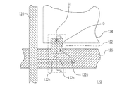
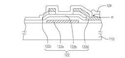
図1は従来技術の既存の画素構造の局所図を概略的に示しており、図2は図1の切断ラインA−A’についての断面図を示している。図1と2は同時に参照する。既存の画素構造120は主に、TFT122、画素電極124、走査線126およびデータ線128を有する。TFT122は、画素電極124と電気的に接続する。詳細には、基板110上のTFT122は、図2に示したように主にゲート122a、チャネル層122b、ソース122cおよびドレイン122dを有する。このTFT122の構造はボトムゲート型に属し、TFT122のドレイン122dは画素電極124と電気的に接続する。図1に見られるように、走査線126とデータ線128を用い、TFT122を介して画素電極124に適切な電圧を送ることができ、画像表示が実現される。
FIG. 1 schematically shows a local view of an existing pixel structure of the prior art, and FIG. 2 shows a cross-sectional view taken along the cutting line A-A 'of FIG. 1 and 2 are referred to simultaneously. The existing
注意すべきことは、ゲート−ドレイン間寄生容量(Cgd)の影響が、ゲート122aとドレイン122dの重複領域10上に通常誘導されるということである。このゲート−ドレイン間寄生容量Cgdの値は、重複領域10の面積に直接的に比例する。TFTの製造では、フォトマスクの位置決め誤差、機械の振動、その他の要因によって、ゲート122aとドレイン122dの重複領域10が変化し、ゲート−ドレイン間寄生容量の値にばらつきを生じる。それにもかかわらず、画素供給電圧はこの値Cgdのばらつきに対応して変化し、画素供給電圧のばらつきによってTFT−LCDの画質が劣化する。
It should be noted that the influence of the gate-drain parasitic capacitance (Cgd) is usually induced on the overlapping
さらに、画素構造の一部に欠陥を引き起こすことがある製造工程中の間違いによって、欠陥を備えた画素構造の修正作業が行われる。一例を挙げる。多くの場合、TFT−LCDがノーマリ・ホワイトモードの場合、画素構造120の修正方法では、ドレイン122dと走査線126を電気的に接続し、ドレイン122dを介して走査線126を画素電極124と電気的に接続できるようにする。そうすることで、画素構造120のドット欠陥を暗点として修正できる。しかし、実際の場合、走査線126(画素電極124)と対向基板の電極の間の電位差が大きくなりすぎることが引き起こしたTFTパネル内の液晶ポリマのオーバツイストの結果、欠陥を備えた画素は灰色の点として現れ、それらは暗点として修正することはできない。
In addition, correction of the pixel structure with the defect is performed due to an error in the manufacturing process that may cause a defect in a part of the pixel structure. Take an example. In many cases, when the TFT-LCD is in the normally white mode, the correction method of the
このことを考慮すると、この発明の一つの目的は、安定した品質を備えた画素構造を提供することである。 In view of this, one object of the present invention is to provide a pixel structure with stable quality.
この発明の別の目的は、この発明の画素構造を修正可能な修正方法を提供し、製品歩留まりを向上させることである。 Another object of the present invention is to provide a correction method capable of correcting the pixel structure of the present invention and to improve the product yield.
この発明の別の一つの目的は、ゲート−ドレイン間寄生容量を一定値に保持可能な薄膜トランジスタを提供することである。 Another object of the present invention is to provide a thin film transistor capable of maintaining a gate-drain parasitic capacitance at a constant value.
この発明は、走査線、ゲートパターン、第一誘電体層、チャネル層、ソース、ドレイン、データ線、第二誘電体層および画素電極を有する画素構造を提供する。前記ゲートパターンは走査線と電気的に接続し、ゲートパターン内には開口部を形成する。第一誘電体層は走査線とゲートパターンを被覆し、開口部を充填する。さらに、チャネル層はゲートパターン上の第一誘電体層上に配置し、チャネル層上にはソースおよびドレインを配置する。ドレインは、開口部上にも配置する。その上、データ線は第一誘電体層上に配置し、データ線はソースと電気的に接続する。第二誘電体層は、ソース、ドレインおよびデータ線を被覆する。さらに、画素電極は第二誘電体層上に配置し、画素電極はドレインと電気的に接続する。 The present invention provides a pixel structure having a scan line, a gate pattern, a first dielectric layer, a channel layer, a source, a drain, a data line, a second dielectric layer, and a pixel electrode. The gate pattern is electrically connected to the scanning line, and an opening is formed in the gate pattern. The first dielectric layer covers the scan line and the gate pattern and fills the opening. Further, the channel layer is disposed on the first dielectric layer on the gate pattern, and the source and drain are disposed on the channel layer. The drain is also disposed on the opening. In addition, the data line is disposed on the first dielectric layer, and the data line is electrically connected to the source. The second dielectric layer covers the source, drain and data lines. Further, the pixel electrode is disposed on the second dielectric layer, and the pixel electrode is electrically connected to the drain.
この発明の好ましい一実施例では、上記の画素構造はさらに、ゲートパターン上を延びる延長ラインを有する。 In a preferred embodiment of the present invention, the pixel structure further has an extension line extending over the gate pattern.
この発明の好ましい一実施例では、上記の画素構造はさらに、チャネル層とソースおよびドレインの間に配置したオーミック接触層を有する。 In one preferred embodiment of the invention, the pixel structure further comprises an ohmic contact layer disposed between the channel layer and the source and drain.
この発明の好ましい一実施例では、前記チャネル層の材料は、例えばアモルファス・シリコンであってもよい。 In a preferred embodiment of the present invention, the material of the channel layer may be amorphous silicon, for example.
この発明の好ましい一実施例では、前記第一誘電体層の材料は、例えば窒化シリコン、酸化シリコン、または酸化窒化シリコン(SiON)であってもよい。 In a preferred embodiment of the present invention, the material of the first dielectric layer may be, for example, silicon nitride, silicon oxide, or silicon oxynitride (SiON).
この発明の好ましい一実施例では、前記第二誘電体層の材料は、例えば窒化シリコン、酸化シリコン、または酸化窒化シリコン(SiON)であってもよい。 In a preferred embodiment of the present invention, the material of the second dielectric layer may be, for example, silicon nitride, silicon oxide, or silicon oxynitride (SiON).
この発明の好ましい一実施例では、前記画素電極の材料は、例えばインジウム錫酸化物(ITO)であってもよい。 In a preferred embodiment of the present invention, the material of the pixel electrode may be indium tin oxide (ITO), for example.
この発明は、上記の画素構造の修正に適した画素修正方法を提供し、前記方法は開口部の周りで、ドレインと延長ラインの両側上のゲートパターンを切断して、ドレインと延長ラインの下に浮遊パターンを形成し、延長ラインと浮遊パターンを電気的に接続し、ドレインと浮遊パターンを電気的に接続するステップを有する。 The present invention provides a pixel correction method suitable for correcting the above-described pixel structure, wherein the method cuts a gate pattern on both sides of the drain and the extension line around the opening so as to be under the drain and the extension line. Forming a floating pattern, electrically connecting the extension line and the floating pattern, and electrically connecting the drain and the floating pattern.
この発明の好ましい一実施例における上記の画素修正方法であって、開口部の周りで、ドレインと延長ラインの両側上のゲートパターンの切断方法はレーザ溝切り技術である。 In the above-described pixel correction method according to a preferred embodiment of the present invention, the gate pattern cutting method on both sides of the drain and the extension line around the opening is a laser grooving technique.
この発明の好ましい一実施例における上記の画素修正方法であって、延長ラインと浮遊パターンを電気的に接続し、ドレインと浮遊パターンを電気的に接続する方法はレーザ溶接技術である。 In the above-described pixel correction method according to a preferred embodiment of the present invention, the method of electrically connecting the extension line and the floating pattern and electrically connecting the drain and the floating pattern is a laser welding technique.
この発明は、ゲートパターン、第一誘電体層、チャネル層、ソース、ドレインおよび第二誘電体層を有する薄膜トランジスタを提供する。ここで、前記ゲートパターン内には開口部を形成し、第一誘電体層はゲートパターンを被覆し、開口部を充填する。さらに、チャネル層はゲートパターン上の第一誘電体層上に配置し、ソースとドレインは両方ともチャネル層上に配置する。前記ドレインは開口部上に配置し、第二誘電体層はソースとドレインを被覆する。 The present invention provides a thin film transistor having a gate pattern, a first dielectric layer, a channel layer, a source, a drain, and a second dielectric layer. Here, an opening is formed in the gate pattern, and the first dielectric layer covers the gate pattern and fills the opening. Further, the channel layer is disposed on the first dielectric layer on the gate pattern, and both the source and the drain are disposed on the channel layer. The drain is disposed on the opening, and the second dielectric layer covers the source and the drain.
この発明の好ましい一実施例における上記薄膜トランジスタのチャネル層の材料は、アモルファス・シリコンであってもよい。 In a preferred embodiment of the present invention, the material of the channel layer of the thin film transistor may be amorphous silicon.
この発明の好ましい一実施例における上記薄膜トランジスタの第一誘電体層の材料は、窒化シリコン、酸化シリコン、または酸化窒化シリコン(SiON)であってもよい。 In one preferred embodiment of the present invention, the material of the first dielectric layer of the thin film transistor may be silicon nitride, silicon oxide, or silicon oxynitride (SiON).
この発明の好ましい一実施例における上記薄膜トランジスタの第二誘電体層の材料は、窒化シリコン、酸化シリコン、または酸化窒化シリコン(SiON)であってもよい。 In a preferred embodiment of the present invention, the material of the second dielectric layer of the thin film transistor may be silicon nitride, silicon oxide, or silicon oxynitride (SiON).
当然のことながら、以上の一般的な説明と以降の詳細な説明は例示的なものであり、請求されるとおりの発明をさらに説明するものとする。 Of course, the foregoing general description and the following detailed description are exemplary and are intended to further describe the invention as claimed.
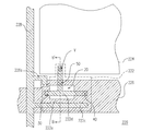
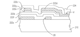
図3は、この発明の好ましい一実施例による画素構造の局所図を概略的に示しており、図4は図3の切断ラインB−B’についての断面図を概略的に示している。図3と4を同時に参照する。この発明の画素構造220は、主に薄膜トランジスタ(TFT)222、画素電極224、走査線226およびデータ線228を有する。
FIG. 3 schematically shows a local view of a pixel structure according to a preferred embodiment of the present invention, and FIG. 4 schematically shows a cross-sectional view taken along the cutting line B-B 'of FIG. Please refer to FIGS. 3 and 4 simultaneously. The
より詳細には、基板210上のTFT222は、図4に示したように画素電極224と電気的に接続する。このTFT222は、ゲートパターン222a、チャネル層222b、ソース222c、ドレイン222d、第一誘電体層222fおよび第二誘電体層222gを有する。ここで、ゲートパターン222aは走査線226と電気的に接続し、開口部20を有する。上記のゲートパターン222aは、例えば走査線226の形成と共に製造し、その間に開口部20を形成する。
More specifically, the TFT 222 on the
さらに、第一誘電体層222fの材料は、例えば窒化シリコン、酸化シリコン、または酸化窒化シリコン(SiON)等の電気的絶縁材料であってもよい。第一誘電体層222fは走査線226とゲートパターン222aを被覆し、開口部20を充填する。上記のチャネル層222bの材料はアモルファス・シリコンであってもよく、ゲートパターン222a上の第一誘電体層222f上に配置する。チャネル層222bのインピーダンスを低減するために、チャネル層222bとソース222cおよびドレイン222dの間に、さらにオーミック接触層222eを形成する。
Further, the material of the first
つまり、ソース222cとドレイン222dはオーミック接触層222e上に配置し、ドレイン222dは開口部20上に配置する。つまり、ドレイン222dは、開口部20上の第一誘電体層222f上に配置する。ここで、ドレイン222dは例えばT字型であってもよく、ゲート−ドレイン間寄生容量の効果はゲートパターン222aとドレイン222dの重複領域(領域30、40および50)内に発生する。
That is, the
さらに、上で議論したように、ドレイン222dは開口部20を横断するように配置する。従って、ドレイン222dの製造工程中、フォトマスクの位置決め誤差や機械の振動によって、T字型のドレイン222dの位置決め場所が水平または垂直にややずれても、重複領域30、40および50の合計の面積は不変のままである。つまり、ゲート−ドレイン間寄生容量Cgdの値は一定に保持され、供給電圧を安定にし、TFT−LCDの画質が維持される。
Further, as discussed above, the
注意すべきことは、この発明では、長方形の開口部20とT字型のドレイン222dを備えた例が取られ、関連図に示されているが、開口部20とドレイン222dの形状はこの発明に限定されないということである。つまり、開口部20とドレイン222dは両方とも他の形状に構成できる。例えば、開口部は円形または多角形等であってもよく、ドレインは長方形や他の形状であってもよい。
It should be noted that in the present invention, an example having a
さらに、上記のデータ線228は第一誘電体層222f上に配置し、ソース222cと電気的に接続する。別の実施例では、データ線228はさらに、データ線228と電気的に接続した延長ライン228aを有する。ソース222c、データ線228および上記の延長ライン228aは共に形成できる。ここで、延長ライン228aはゲートパターン222a上に延び、以降で詳しく説明するように、延長ライン228aの利用目的はレーザ修正に役立たせることである。
Further, the
さらに、第二誘電体層222gの材料は、例えば窒化シリコン、酸化シリコン、または酸化窒化シリコン(SiON)であってもよい。そして、第二誘電体層222gは、ソース222c、ドレイン222dおよびデータ線228を被覆する。この実施例の画素電極224は第二誘電体層222g上に配置し、コンタクト窓Vを介して、ドレイン222dと電気的に接続する。
Further, the material of the
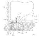
製造工程または静電気損傷等の要因が、図3の画素構造内の欠陥を引き起こすとした場合、図3の画素構造220を修正方法は次のとおりである。まず、図3を参照し、開口部20の周りで、ドレイン222dと延長ライン228aの片側のゲートパターン222aを切断し、図5Aに示したように、ドレイン222dと延長ライン228aの下部で、ゲートパターン222aの一部を浮遊パターンPとして形成する。上記のゲートパターン222aの切断方法は、レーザ溝切り技術であってもよい。この浮遊パターンPは、ゲートパターン222aから電気的に絶縁される。
If a factor such as a manufacturing process or electrostatic damage causes a defect in the pixel structure of FIG. 3, a method of correcting the
次に、図5Bに示したように、延長ライン228aと浮遊パターンPを電気的に接続し、ドレイン222dと浮遊パターンPを電気的に接続する。上記の電気的に接続を行う方法は、レーザ溶接技術である。そうすることで、データ線228は、延長ライン228aと浮遊パターンPを介して、ドレイン222dと電気的に接続できる。その後、図6を参照すると、図5の切断ラインC−C’についての断面図が概略的に示されている。延長ライン228aと浮遊パターンPを電気的に接続することで、画素電極224はデータ線228と電気的に接続される。
Next, as shown in FIG. 5B, the
通常、対向基板上の電極とデータ線228の間の電位差は、対向基板上の電極と走査線226の間の電位差より小さい。従って、画素電極と走査線を電気的に接続する既存の修正方法に比べて、レーザ溶接技術を用いて、画素電極224とデータ線228を電気的に接続することによる画素修正は、画素電極224と対向基板の電極の間の電位差が大きくなりすぎることを防ぐことができる。この方法では、画素の液晶分子のオーバツイストを防ぐことができる。その結果、ノーマリ・ホワイトモードのTFT−LCD用のドット欠陥を備えた画素構造を修正後、それに対応して表示領域内に暗点を形成でき、従って画素構造の修正が実現できる。
Usually, the potential difference between the electrode on the counter substrate and the
つまり、この発明の画素構造およびその修正方法は、少なくとも次のような利点を有する。
(i)この発明の画素構造内ではゲートパターンが開口部を備え、前記開口部上にドレインを配置したTFTを採用することで、ゲート−ドレイン間寄生容量を一定に保持する。
(ii)この発明に基づく画素構造の修正方法を用いることで、ドット欠陥を備えた画素を暗点として修正できる。
That is, the pixel structure of the present invention and the correction method thereof have at least the following advantages.
(I) In the pixel structure of the present invention, a gate pattern is provided with an opening, and a TFT having a drain disposed on the opening is employed, so that the gate-drain parasitic capacitance is kept constant.
(Ii) By using the pixel structure correcting method according to the present invention, a pixel having a dot defect can be corrected as a dark spot.
当業者には明らかなように、発明の範囲または精神から逸脱することなく、この発明の構造に様々な修正および変更を行うことができる。上記の観点から、添付の請求項およびそれらと等価なものの範囲内にある限り、この発明はその修正および変形を含むものとする。 It will be apparent to those skilled in the art that various modifications and variations can be made to the structure of the present invention without departing from the scope or spirit of the invention. In view of the above, the present invention is intended to include modifications and variations thereof as long as they are within the scope of the appended claims and their equivalents.
添付の図面は、発明をさらに理解するために含められ、この明細書に組み込まれ、その一部を構成する。図面は発明の実施例を示し、開示内容と共に、発明の原理の説明に役立つ。 The accompanying drawings are included to provide a further understanding of the invention, and are incorporated in and constitute a part of this specification. The drawings illustrate embodiments of the invention and, together with the disclosure, serve to explain the principles of the invention.
10 重複領域
20 開口部
30 重複領域
110 基板
120 画素構造
122a ゲート
122b チャネル層
122c ソース
122d ドレイン
124 画素電極
126 走査線
128 データ線
210 基板
220 画素構造
222a ゲートパターン
222b チャネル層
222c ソース
222d ドレイン
222e オーミック接触層
222f 第一誘電体層
222g 第二誘電体層
224 画素電極
226 走査線
228 データ線
228a 延長ライン
A−A’ 切断ライン
B−B’ 切断ライン
C−C’ 切断ライン
P 浮遊パターン
V コンタクト窓
10
Claims (15)
走査線に電気的に接続し、内側に開口部を形成したゲートパターンと、
走査線およびゲートパターンを被覆し、開口部を充填する第一誘電体層と、
ゲートパターン上方で第一誘電体層上に配置したチャネル層と、
チャネル層上に配置したソースおよびドレインと、
第一誘電体層上に配置し、ソースと電気的に接続したデータ線と、
ソース、ドレインおよびデータ線を被覆する第二誘電体層と、
第二誘電体層上に配置し、ドレインに電気的に接続した画素電極を有し、
前記開口部上方にドレインを配置した画素構造。 Scanning lines;
A gate pattern electrically connected to the scanning line and having an opening formed inside;
A first dielectric layer covering the scan line and the gate pattern and filling the opening;
A channel layer disposed on the first dielectric layer above the gate pattern;
A source and a drain disposed on the channel layer;
A data line disposed on the first dielectric layer and electrically connected to the source;
A second dielectric layer covering the source, drain and data lines;
A pixel electrode disposed on the second dielectric layer and electrically connected to the drain;
A pixel structure in which a drain is disposed above the opening.
延長ラインと浮遊パターンを電気的に接続し、
ドレインと浮遊パターンを電気的に接続する請求項2記載の画素構造の修正に適した画素修正方法。 Around the opening, cut the gate pattern on both sides of the drain and extension line, forming a floating pattern under the drain and extension line,
Connect the extension line and the floating pattern electrically,
3. The pixel correction method suitable for correcting a pixel structure according to claim 2, wherein the drain and the floating pattern are electrically connected.
ゲートパターンを被覆し、開口部を充填する第一誘電体層と、
ゲートパターン上の第一誘電体層上に配置したチャネル層と、
チャネル層上に配置したソースおよびドレインと、
ソースおよびドレインを被覆する第二誘電体層を有し、前記開口部上にドレインを配置した薄膜トランジスタ。 A gate pattern in which an opening is formed, and
A first dielectric layer covering the gate pattern and filling the opening;
A channel layer disposed on the first dielectric layer on the gate pattern;
A source and a drain disposed on the channel layer;
A thin film transistor having a second dielectric layer covering the source and the drain and having the drain disposed on the opening.
Applications Claiming Priority (1)
| Application Number | Priority Date | Filing Date | Title |
|---|---|---|---|
| TW094137106A TWI271870B (en) | 2005-10-24 | 2005-10-24 | Thin film transistor, pixel structure and repairing method thereof |
Publications (1)
| Publication Number | Publication Date |
|---|---|
| JP2007123794A true JP2007123794A (en) | 2007-05-17 |
Family
ID=36603848
Family Applications (1)
| Application Number | Title | Priority Date | Filing Date |
|---|---|---|---|
| JP2006009125A Pending JP2007123794A (en) | 2005-10-24 | 2006-01-17 | Thin film transistor, pixel structure, and correction method thereof |
Country Status (6)
| Country | Link |
|---|---|
| US (1) | US7427777B2 (en) |
| JP (1) | JP2007123794A (en) |
| DE (1) | DE102006020217A1 (en) |
| FR (1) | FR2892531B1 (en) |
| GB (1) | GB2431514B (en) |
| TW (1) | TWI271870B (en) |
Families Citing this family (16)
| Publication number | Priority date | Publication date | Assignee | Title |
|---|---|---|---|---|
| US8089574B2 (en) * | 2005-12-15 | 2012-01-03 | Sharp Kabushiki Kaisha | Active matrix substrate, display, and television receiver |
| TWI277216B (en) * | 2006-02-16 | 2007-03-21 | Au Optronics Corp | Pixel structure and thin film transistor and fabrication methods thereof |
| US20070194331A1 (en) * | 2006-02-17 | 2007-08-23 | Yeh Chang C | Liquid crystal display device and defect repairing method for the same |
| TWI293802B (en) * | 2006-03-28 | 2008-02-21 | Au Optronics Corp | Liquid crystal display device |
| US7688392B2 (en) * | 2006-04-06 | 2010-03-30 | Chunghwa Picture Tubes, Ltd. | Pixel structure including a gate having an opening and an extension line between the data line and the source |
| TWI333587B (en) * | 2006-09-15 | 2010-11-21 | Chunghwa Picture Tubes Ltd | Pixel structure and repair method thereof |
| TWI354172B (en) * | 2007-03-21 | 2011-12-11 | Au Optronics Corp | Pixel array substrate |
| JP5157319B2 (en) * | 2007-08-28 | 2013-03-06 | セイコーエプソン株式会社 | Electro-optical device and electronic apparatus |
| TWI463465B (en) * | 2008-04-09 | 2014-12-01 | Chunghwa Picture Tubes Ltd | Repairing method |
| CN100583459C (en) * | 2008-09-24 | 2010-01-20 | 友达光电股份有限公司 | pixel structure and thin film transistor thereof |
| TW201039034A (en) * | 2009-04-27 | 2010-11-01 | Chunghwa Picture Tubes Ltd | Pixel structure and the method of forming the same |
| TWI402596B (en) * | 2009-10-01 | 2013-07-21 | Chunghwa Picture Tubes Ltd | Pixel structure with capacitance compensation |
| KR101623961B1 (en) * | 2009-12-02 | 2016-05-26 | 삼성전자주식회사 | Transistor, method of manufacturing the same and electronic device comprising transistor |
| KR101902922B1 (en) * | 2011-03-03 | 2018-10-02 | 삼성전자주식회사 | Thin film transistor and manufacturing method of the same |
| US8988624B2 (en) * | 2011-06-23 | 2015-03-24 | Apple Inc. | Display pixel having oxide thin-film transistor (TFT) with reduced loading |
| CN110931504A (en) * | 2019-09-17 | 2020-03-27 | 深圳市华星光电半导体显示技术有限公司 | Array substrate and display panel |
Family Cites Families (9)
| Publication number | Priority date | Publication date | Assignee | Title |
|---|---|---|---|---|
| KR100214074B1 (en) * | 1995-11-03 | 1999-08-02 | 김영환 | A thin film transistor and manufacturing method thereof |
| US5808317A (en) * | 1996-07-24 | 1998-09-15 | International Business Machines Corporation | Split-gate, horizontally redundant, and self-aligned thin film transistors |
| JP3036513B2 (en) * | 1998-06-10 | 2000-04-24 | 日本電気株式会社 | Liquid crystal display |
| KR100542310B1 (en) * | 1998-12-30 | 2006-05-09 | 비오이 하이디스 테크놀로지 주식회사 | Thin film transistor liquid crystal display |
| KR100370800B1 (en) * | 2000-06-09 | 2003-02-05 | 엘지.필립스 엘시디 주식회사 | method for fabricating array substrate for LCD |
| KR100450701B1 (en) * | 2001-12-28 | 2004-10-01 | 엘지.필립스 엘시디 주식회사 | The substrate for LCD and method for fabricating the same |
| WO2004063799A1 (en) * | 2002-12-03 | 2004-07-29 | Quanta Display Inc. | Method for manufacturing the thin film transistor array |
| KR100904523B1 (en) * | 2002-12-26 | 2009-06-25 | 엘지디스플레이 주식회사 | Thin Film Transistor for Active Matrix Organic Light Emitting Diode |
| CN1331241C (en) | 2003-08-12 | 2007-08-08 | 友达光电股份有限公司 | Thin film transistor and pixel structure with such thin film transistor |
-
2005
- 2005-10-24 TW TW094137106A patent/TWI271870B/en not_active IP Right Cessation
- 2005-12-08 US US11/164,856 patent/US7427777B2/en not_active Expired - Lifetime
-
2006
- 2006-01-17 JP JP2006009125A patent/JP2007123794A/en active Pending
- 2006-05-02 DE DE102006020217A patent/DE102006020217A1/en not_active Withdrawn
- 2006-05-03 GB GB0608742A patent/GB2431514B/en not_active Expired - Fee Related
- 2006-05-24 FR FR0604715A patent/FR2892531B1/en not_active Expired - Fee Related
Also Published As
| Publication number | Publication date |
|---|---|
| US20070090357A1 (en) | 2007-04-26 |
| US7427777B2 (en) | 2008-09-23 |
| TWI271870B (en) | 2007-01-21 |
| TW200717809A (en) | 2007-05-01 |
| FR2892531A1 (en) | 2007-04-27 |
| GB2431514B (en) | 2008-03-19 |
| DE102006020217A1 (en) | 2007-04-26 |
| GB0608742D0 (en) | 2006-06-14 |
| GB2431514A (en) | 2007-04-25 |
| FR2892531B1 (en) | 2009-03-20 |
Similar Documents
| Publication | Publication Date | Title |
|---|---|---|
| JP2007123794A (en) | Thin film transistor, pixel structure, and correction method thereof | |
| US8988621B2 (en) | Array substrate and display panel having the same | |
| US8130333B2 (en) | Electric optical device and electronic device | |
| WO2002031887A1 (en) | Transistor and display comprising it | |
| US8199266B2 (en) | Pixel structure, driving method thereof, pixel array structure, and liquid crystal display panel | |
| US20100320473A1 (en) | Thin film transistor structure of pixel | |
| JP4642700B2 (en) | Pixel structure and repair method thereof | |
| US8134155B2 (en) | Liquid crystal display device capable of reducing leakage current, and fabrication method thereof | |
| US6580093B2 (en) | Structure of a thin film transistor (TFT) array | |
| US20080100767A1 (en) | Pixel structure and method for repairing same | |
| CN100444383C (en) | Thin film transistor, pixel structure and method for repairing pixel structure | |
| JP2006250985A (en) | Electrooptical apparatus and electronic device | |
| US6806927B2 (en) | Step-eliminating film and island-shaped pattern composed of conductive film for a reflective electrooptic device and electronic apparatus | |
| CN100502051C (en) | Thin film transistor array and repairing method thereof | |
| JP2007114729A (en) | Liquid crystal display device | |
| CN100594407C (en) | Array substrate, manufacturing method thereof, and display using the substrate | |
| US7570311B2 (en) | Electro-optical device, electronic apparatus, and method of manufacturing electro-optical device having particular capacitive elements | |
| JP2007164172A (en) | Liquid crystal display and method of manufacturing liquid crystal display | |
| US20070200111A1 (en) | Image display device | |
| US6838699B2 (en) | Electro-optical device with undercut-reducing thin film pattern and reticle | |
| US7633568B2 (en) | Pixel structure | |
| JP4078928B2 (en) | Electro-optical device and electronic apparatus | |
| JP2002297058A (en) | Active matrix display | |
| CN101738805A (en) | Pixel structure | |
| JP5162232B2 (en) | Display device |
Legal Events
| Date | Code | Title | Description |
|---|---|---|---|
| A977 | Report on retrieval |
Free format text: JAPANESE INTERMEDIATE CODE: A971007 Effective date: 20090226 |
|
| A131 | Notification of reasons for refusal |
Free format text: JAPANESE INTERMEDIATE CODE: A131 Effective date: 20090305 |
|
| A521 | Request for written amendment filed |
Free format text: JAPANESE INTERMEDIATE CODE: A523 Effective date: 20090605 |
|
| RD04 | Notification of resignation of power of attorney |
Free format text: JAPANESE INTERMEDIATE CODE: A7424 Effective date: 20091112 |
|
| A02 | Decision of refusal |
Free format text: JAPANESE INTERMEDIATE CODE: A02 Effective date: 20091215 |