JP2007123794A - 薄膜トランジスタ、画素構造およびその修正方法 - Google Patents
薄膜トランジスタ、画素構造およびその修正方法 Download PDFInfo
- Publication number
- JP2007123794A JP2007123794A JP2006009125A JP2006009125A JP2007123794A JP 2007123794 A JP2007123794 A JP 2007123794A JP 2006009125 A JP2006009125 A JP 2006009125A JP 2006009125 A JP2006009125 A JP 2006009125A JP 2007123794 A JP2007123794 A JP 2007123794A
- Authority
- JP
- Japan
- Prior art keywords
- drain
- dielectric layer
- disposed
- opening
- gate pattern
- Prior art date
- Legal status (The legal status is an assumption and is not a legal conclusion. Google has not performed a legal analysis and makes no representation as to the accuracy of the status listed.)
- Pending
Links
Images


Classifications
-
- G—PHYSICS
- G02—OPTICS
- G02F—OPTICAL DEVICES OR ARRANGEMENTS FOR THE CONTROL OF LIGHT BY MODIFICATION OF THE OPTICAL PROPERTIES OF THE MEDIA OF THE ELEMENTS INVOLVED THEREIN; NON-LINEAR OPTICS; FREQUENCY-CHANGING OF LIGHT; OPTICAL LOGIC ELEMENTS; OPTICAL ANALOGUE/DIGITAL CONVERTERS
- G02F1/00—Devices or arrangements for the control of the intensity, colour, phase, polarisation or direction of light arriving from an independent light source, e.g. switching, gating or modulating; Non-linear optics
- G02F1/01—Devices or arrangements for the control of the intensity, colour, phase, polarisation or direction of light arriving from an independent light source, e.g. switching, gating or modulating; Non-linear optics for the control of the intensity, phase, polarisation or colour
- G02F1/13—Devices or arrangements for the control of the intensity, colour, phase, polarisation or direction of light arriving from an independent light source, e.g. switching, gating or modulating; Non-linear optics for the control of the intensity, phase, polarisation or colour based on liquid crystals, e.g. single liquid crystal display cells
- G02F1/133—Constructional arrangements; Operation of liquid crystal cells; Circuit arrangements
- G02F1/136—Liquid crystal cells structurally associated with a semi-conducting layer or substrate, e.g. cells forming part of an integrated circuit
- G02F1/1362—Active matrix addressed cells
-
- H—ELECTRICITY
- H10—SEMICONDUCTOR DEVICES; ELECTRIC SOLID-STATE DEVICES NOT OTHERWISE PROVIDED FOR
- H10D—INORGANIC ELECTRIC SEMICONDUCTOR DEVICES
- H10D86/00—Integrated devices formed in or on insulating or conducting substrates, e.g. formed in silicon-on-insulator [SOI] substrates or on stainless steel or glass substrates
-
- G—PHYSICS
- G02—OPTICS
- G02F—OPTICAL DEVICES OR ARRANGEMENTS FOR THE CONTROL OF LIGHT BY MODIFICATION OF THE OPTICAL PROPERTIES OF THE MEDIA OF THE ELEMENTS INVOLVED THEREIN; NON-LINEAR OPTICS; FREQUENCY-CHANGING OF LIGHT; OPTICAL LOGIC ELEMENTS; OPTICAL ANALOGUE/DIGITAL CONVERTERS
- G02F1/00—Devices or arrangements for the control of the intensity, colour, phase, polarisation or direction of light arriving from an independent light source, e.g. switching, gating or modulating; Non-linear optics
- G02F1/01—Devices or arrangements for the control of the intensity, colour, phase, polarisation or direction of light arriving from an independent light source, e.g. switching, gating or modulating; Non-linear optics for the control of the intensity, phase, polarisation or colour
- G02F1/13—Devices or arrangements for the control of the intensity, colour, phase, polarisation or direction of light arriving from an independent light source, e.g. switching, gating or modulating; Non-linear optics for the control of the intensity, phase, polarisation or colour based on liquid crystals, e.g. single liquid crystal display cells
- G02F1/133—Constructional arrangements; Operation of liquid crystal cells; Circuit arrangements
- G02F1/136—Liquid crystal cells structurally associated with a semi-conducting layer or substrate, e.g. cells forming part of an integrated circuit
- G02F1/1362—Active matrix addressed cells
- G02F1/136259—Repairing; Defects
-
- H—ELECTRICITY
- H10—SEMICONDUCTOR DEVICES; ELECTRIC SOLID-STATE DEVICES NOT OTHERWISE PROVIDED FOR
- H10D—INORGANIC ELECTRIC SEMICONDUCTOR DEVICES
- H10D30/00—Field-effect transistors [FET]
- H10D30/60—Insulated-gate field-effect transistors [IGFET]
- H10D30/67—Thin-film transistors [TFT]
-
- H—ELECTRICITY
- H10—SEMICONDUCTOR DEVICES; ELECTRIC SOLID-STATE DEVICES NOT OTHERWISE PROVIDED FOR
- H10D—INORGANIC ELECTRIC SEMICONDUCTOR DEVICES
- H10D30/00—Field-effect transistors [FET]
- H10D30/60—Insulated-gate field-effect transistors [IGFET]
- H10D30/67—Thin-film transistors [TFT]
- H10D30/6729—Thin-film transistors [TFT] characterised by the electrodes
- H10D30/673—Thin-film transistors [TFT] characterised by the electrodes characterised by the shapes, relative sizes or dispositions of the gate electrodes
- H10D30/6732—Bottom-gate only TFTs
-
- H—ELECTRICITY
- H10—SEMICONDUCTOR DEVICES; ELECTRIC SOLID-STATE DEVICES NOT OTHERWISE PROVIDED FOR
- H10D—INORGANIC ELECTRIC SEMICONDUCTOR DEVICES
- H10D30/00—Field-effect transistors [FET]
- H10D30/60—Insulated-gate field-effect transistors [IGFET]
- H10D30/67—Thin-film transistors [TFT]
- H10D30/674—Thin-film transistors [TFT] characterised by the active materials
- H10D30/6741—Group IV materials, e.g. germanium or silicon carbide
- H10D30/6743—Silicon
- H10D30/6746—Amorphous silicon
-
- H—ELECTRICITY
- H10—SEMICONDUCTOR DEVICES; ELECTRIC SOLID-STATE DEVICES NOT OTHERWISE PROVIDED FOR
- H10D—INORGANIC ELECTRIC SEMICONDUCTOR DEVICES
- H10D86/00—Integrated devices formed in or on insulating or conducting substrates, e.g. formed in silicon-on-insulator [SOI] substrates or on stainless steel or glass substrates
- H10D86/40—Integrated devices formed in or on insulating or conducting substrates, e.g. formed in silicon-on-insulator [SOI] substrates or on stainless steel or glass substrates characterised by multiple TFTs
- H10D86/441—Interconnections, e.g. scanning lines
-
- H—ELECTRICITY
- H10—SEMICONDUCTOR DEVICES; ELECTRIC SOLID-STATE DEVICES NOT OTHERWISE PROVIDED FOR
- H10D—INORGANIC ELECTRIC SEMICONDUCTOR DEVICES
- H10D86/00—Integrated devices formed in or on insulating or conducting substrates, e.g. formed in silicon-on-insulator [SOI] substrates or on stainless steel or glass substrates
- H10D86/40—Integrated devices formed in or on insulating or conducting substrates, e.g. formed in silicon-on-insulator [SOI] substrates or on stainless steel or glass substrates characterised by multiple TFTs
- H10D86/60—Integrated devices formed in or on insulating or conducting substrates, e.g. formed in silicon-on-insulator [SOI] substrates or on stainless steel or glass substrates characterised by multiple TFTs wherein the TFTs are in active matrices
Landscapes
- Physics & Mathematics (AREA)
- Nonlinear Science (AREA)
- Engineering & Computer Science (AREA)
- Microelectronics & Electronic Packaging (AREA)
- Mathematical Physics (AREA)
- Chemical & Material Sciences (AREA)
- Crystallography & Structural Chemistry (AREA)
- General Physics & Mathematics (AREA)
- Optics & Photonics (AREA)
- Thin Film Transistor (AREA)
- Liquid Crystal (AREA)
Abstract
【解決手段】
走査線、ゲートパターン、第一誘電体層、チャネル層、ソース、ドレイン、データ線、第二誘電体層および画素電極を有する画素構造が提供される。ゲートパターンは走査線と電気的に接続し、内部に開口部を備えている。第一誘電体層は走査線とゲートパターンを被覆し、開口部を充填する。さらに、チャネル層は第一誘電体層上に配置し、ソースおよびドレインはチャネル層上に配置する。ドレインは、ゲートパターンの開口部上に配置する。ソースはデータ線と電気的に接続し、画素電極はドレインと電気的に接続する。開口部を備えたゲートパターンとドレインの間の重複領域は、ゲート−ドレイン間の容量(Cgd)を変化させないように保持できる。
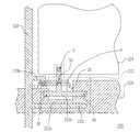
【選択図】 図3
Description
(i)この発明の画素構造内ではゲートパターンが開口部を備え、前記開口部上にドレインを配置したTFTを採用することで、ゲート−ドレイン間寄生容量を一定に保持する。
(ii)この発明に基づく画素構造の修正方法を用いることで、ドット欠陥を備えた画素を暗点として修正できる。
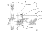
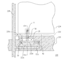
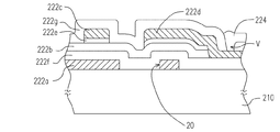
20 開口部
30 重複領域
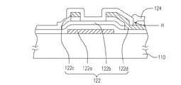
110 基板
120 画素構造
122a ゲート
122b チャネル層
122c ソース
122d ドレイン
124 画素電極
126 走査線
128 データ線
210 基板
220 画素構造
222a ゲートパターン
222b チャネル層
222c ソース
222d ドレイン
222e オーミック接触層
222f 第一誘電体層
222g 第二誘電体層
224 画素電極
226 走査線
228 データ線
228a 延長ライン
A−A’ 切断ライン
B−B’ 切断ライン
C−C’ 切断ライン
P 浮遊パターン
V コンタクト窓
Claims (15)
- 走査線と、
走査線に電気的に接続し、内側に開口部を形成したゲートパターンと、
走査線およびゲートパターンを被覆し、開口部を充填する第一誘電体層と、
ゲートパターン上方で第一誘電体層上に配置したチャネル層と、
チャネル層上に配置したソースおよびドレインと、
第一誘電体層上に配置し、ソースと電気的に接続したデータ線と、
ソース、ドレインおよびデータ線を被覆する第二誘電体層と、
第二誘電体層上に配置し、ドレインに電気的に接続した画素電極を有し、
前記開口部上方にドレインを配置した画素構造。 - さらに、データ線と電気的に接続し、ゲートパターン上方に延びる延長ラインを有する請求項1記載の画素構造。
- さらに、チャネル層とソースおよびドレインの間に配置したオーミック接触層を有する請求項1記載の画素構造。
- チャネル層の材料が、アモルファス・シリコンを含む請求項1記載の画素構造。
- 第一誘電体層の材料が、窒化シリコン、酸化シリコン、および酸化窒化シリコン(SiON)を含む請求項1記載の画素構造。
- 第二誘電体層の材料が、窒化シリコン、酸化シリコン、および酸化窒化シリコン(SiON)を含む請求項1記載の画素構造。
- 画素電極の材料が、インジウム錫酸化物(ITO)を含む請求項1記載の画素構造。
- 開口部の周りで、ドレインと延長ラインの両側のゲートパターンを切断し、ドレインおよび延長ラインの下に浮遊パターンを形成し、
延長ラインと浮遊パターンを電気的に接続し、
ドレインと浮遊パターンを電気的に接続する請求項2記載の画素構造の修正に適した画素修正方法。 - 開口部の周りで、ドレインおよび延長ラインの両側のゲートパターンを切断する方法が、レーザ溝切り技術である請求項8記載の画素修正方法。
- 延長ラインと浮遊パターンを電気的に接続し、ドレインと浮遊パターンを電気的に接続する方法が、レーザ溶接技術である請求項8記載の画素修正方法。
- 内部に開口部を形成したゲートパターンと、
ゲートパターンを被覆し、開口部を充填する第一誘電体層と、
ゲートパターン上の第一誘電体層上に配置したチャネル層と、
チャネル層上に配置したソースおよびドレインと、
ソースおよびドレインを被覆する第二誘電体層を有し、前記開口部上にドレインを配置した薄膜トランジスタ。 - さらに、チャネル層とソースおよびドレインの間に配置したオーミック接触層を有する請求項11記載の薄膜トランジスタ。
- チャネル層の材料が、アモルファス・シリコンを含む請求項11記載の薄膜トランジスタ。
- 第一誘電体層の材料が、窒化シリコン、酸化シリコン、および酸化窒化シリコン(SiON)を含む請求項11記載の薄膜トランジスタ。
- 第二誘電体層の材料が、窒化シリコン、酸化シリコン、および酸化窒化シリコン(SiON)を含む請求項11記載の薄膜トランジスタ。
Applications Claiming Priority (1)
| Application Number | Priority Date | Filing Date | Title |
|---|---|---|---|
| TW094137106A TWI271870B (en) | 2005-10-24 | 2005-10-24 | Thin film transistor, pixel structure and repairing method thereof |
Publications (1)
| Publication Number | Publication Date |
|---|---|
| JP2007123794A true JP2007123794A (ja) | 2007-05-17 |
Family
ID=36603848
Family Applications (1)
| Application Number | Title | Priority Date | Filing Date |
|---|---|---|---|
| JP2006009125A Pending JP2007123794A (ja) | 2005-10-24 | 2006-01-17 | 薄膜トランジスタ、画素構造およびその修正方法 |
Country Status (6)
| Country | Link |
|---|---|
| US (1) | US7427777B2 (ja) |
| JP (1) | JP2007123794A (ja) |
| DE (1) | DE102006020217A1 (ja) |
| FR (1) | FR2892531B1 (ja) |
| GB (1) | GB2431514B (ja) |
| TW (1) | TWI271870B (ja) |
Families Citing this family (16)
| Publication number | Priority date | Publication date | Assignee | Title |
|---|---|---|---|---|
| US8089574B2 (en) * | 2005-12-15 | 2012-01-03 | Sharp Kabushiki Kaisha | Active matrix substrate, display, and television receiver |
| TWI277216B (en) * | 2006-02-16 | 2007-03-21 | Au Optronics Corp | Pixel structure and thin film transistor and fabrication methods thereof |
| US20070194331A1 (en) * | 2006-02-17 | 2007-08-23 | Yeh Chang C | Liquid crystal display device and defect repairing method for the same |
| TWI293802B (en) * | 2006-03-28 | 2008-02-21 | Au Optronics Corp | Liquid crystal display device |
| US7688392B2 (en) * | 2006-04-06 | 2010-03-30 | Chunghwa Picture Tubes, Ltd. | Pixel structure including a gate having an opening and an extension line between the data line and the source |
| TWI333587B (en) * | 2006-09-15 | 2010-11-21 | Chunghwa Picture Tubes Ltd | Pixel structure and repair method thereof |
| TWI354172B (en) * | 2007-03-21 | 2011-12-11 | Au Optronics Corp | Pixel array substrate |
| JP5157319B2 (ja) * | 2007-08-28 | 2013-03-06 | セイコーエプソン株式会社 | 電気光学装置及び電子機器 |
| TWI463465B (zh) * | 2008-04-09 | 2014-12-01 | Chunghwa Picture Tubes Ltd | 修補方法 |
| CN100583459C (zh) * | 2008-09-24 | 2010-01-20 | 友达光电股份有限公司 | 像素结构及其薄膜晶体管 |
| TW201039034A (en) * | 2009-04-27 | 2010-11-01 | Chunghwa Picture Tubes Ltd | Pixel structure and the method of forming the same |
| TWI402596B (zh) * | 2009-10-01 | 2013-07-21 | Chunghwa Picture Tubes Ltd | 具有電容補償的畫素結構 |
| KR101623961B1 (ko) * | 2009-12-02 | 2016-05-26 | 삼성전자주식회사 | 트랜지스터와 그 제조방법 및 트랜지스터를 포함하는 전자소자 |
| KR101902922B1 (ko) * | 2011-03-03 | 2018-10-02 | 삼성전자주식회사 | 박막 트랜지스터 및 박막 트랜지스터의 제조 방법 |
| US8988624B2 (en) * | 2011-06-23 | 2015-03-24 | Apple Inc. | Display pixel having oxide thin-film transistor (TFT) with reduced loading |
| CN110931504A (zh) * | 2019-09-17 | 2020-03-27 | 深圳市华星光电半导体显示技术有限公司 | 阵列基板及显示面板 |
Family Cites Families (9)
| Publication number | Priority date | Publication date | Assignee | Title |
|---|---|---|---|---|
| KR100214074B1 (ko) * | 1995-11-03 | 1999-08-02 | 김영환 | 박막트랜지스터 및 그 제조방법 |
| US5808317A (en) * | 1996-07-24 | 1998-09-15 | International Business Machines Corporation | Split-gate, horizontally redundant, and self-aligned thin film transistors |
| JP3036513B2 (ja) * | 1998-06-10 | 2000-04-24 | 日本電気株式会社 | 液晶表示装置 |
| KR100542310B1 (ko) * | 1998-12-30 | 2006-05-09 | 비오이 하이디스 테크놀로지 주식회사 | 박막 트랜지스터 액정표시소자_ |
| KR100370800B1 (ko) * | 2000-06-09 | 2003-02-05 | 엘지.필립스 엘시디 주식회사 | 액정표시장치용 어레이기판 제작방법 |
| KR100450701B1 (ko) * | 2001-12-28 | 2004-10-01 | 엘지.필립스 엘시디 주식회사 | 액정표시장치용 어레이기판과 그 제조방법 |
| WO2004063799A1 (fr) * | 2002-12-03 | 2004-07-29 | Quanta Display Inc. | Procede de fabrication d'un reseau de transistors en couches minces |
| KR100904523B1 (ko) * | 2002-12-26 | 2009-06-25 | 엘지디스플레이 주식회사 | 액티브 매트릭스형 유기전계발광 소자용 박막트랜지스터 |
| CN1331241C (zh) | 2003-08-12 | 2007-08-08 | 友达光电股份有限公司 | 薄膜晶体管及具有此种薄膜晶体管的像素结构 |
-
2005
- 2005-10-24 TW TW094137106A patent/TWI271870B/zh not_active IP Right Cessation
- 2005-12-08 US US11/164,856 patent/US7427777B2/en not_active Expired - Lifetime
-
2006
- 2006-01-17 JP JP2006009125A patent/JP2007123794A/ja active Pending
- 2006-05-02 DE DE102006020217A patent/DE102006020217A1/de not_active Withdrawn
- 2006-05-03 GB GB0608742A patent/GB2431514B/en not_active Expired - Fee Related
- 2006-05-24 FR FR0604715A patent/FR2892531B1/fr not_active Expired - Fee Related
Also Published As
| Publication number | Publication date |
|---|---|
| US20070090357A1 (en) | 2007-04-26 |
| US7427777B2 (en) | 2008-09-23 |
| TWI271870B (en) | 2007-01-21 |
| TW200717809A (en) | 2007-05-01 |
| FR2892531A1 (fr) | 2007-04-27 |
| GB2431514B (en) | 2008-03-19 |
| DE102006020217A1 (de) | 2007-04-26 |
| GB0608742D0 (en) | 2006-06-14 |
| GB2431514A (en) | 2007-04-25 |
| FR2892531B1 (fr) | 2009-03-20 |
Similar Documents
| Publication | Publication Date | Title |
|---|---|---|
| JP2007123794A (ja) | 薄膜トランジスタ、画素構造およびその修正方法 | |
| US8988621B2 (en) | Array substrate and display panel having the same | |
| US8130333B2 (en) | Electric optical device and electronic device | |
| WO2002031887A1 (en) | Transistor and display comprising it | |
| US8199266B2 (en) | Pixel structure, driving method thereof, pixel array structure, and liquid crystal display panel | |
| US20100320473A1 (en) | Thin film transistor structure of pixel | |
| JP4642700B2 (ja) | 画素構造体とその修理方法 | |
| US8134155B2 (en) | Liquid crystal display device capable of reducing leakage current, and fabrication method thereof | |
| US6580093B2 (en) | Structure of a thin film transistor (TFT) array | |
| US20080100767A1 (en) | Pixel structure and method for repairing same | |
| CN100444383C (zh) | 薄膜晶体管、像素结构及像素结构之修补方法 | |
| JP2006250985A (ja) | 電気光学装置及び電子機器 | |
| US6806927B2 (en) | Step-eliminating film and island-shaped pattern composed of conductive film for a reflective electrooptic device and electronic apparatus | |
| CN100502051C (zh) | 薄膜晶体管阵列及其修补方法 | |
| JP2007114729A (ja) | 液晶表示装置 | |
| CN100594407C (zh) | 阵列基板及其制造方法和采用该基板的显示器 | |
| US7570311B2 (en) | Electro-optical device, electronic apparatus, and method of manufacturing electro-optical device having particular capacitive elements | |
| JP2007164172A (ja) | 液晶ディスプレイ、及び液晶ディスプレイの製造方法 | |
| US20070200111A1 (en) | Image display device | |
| US6838699B2 (en) | Electro-optical device with undercut-reducing thin film pattern and reticle | |
| US7633568B2 (en) | Pixel structure | |
| JP4078928B2 (ja) | 電気光学装置および電子機器 | |
| JP2002297058A (ja) | アクティブマトリクス型表示装置 | |
| CN101738805A (zh) | 像素结构 | |
| JP5162232B2 (ja) | 表示装置 |
Legal Events
| Date | Code | Title | Description |
|---|---|---|---|
| A977 | Report on retrieval |
Free format text: JAPANESE INTERMEDIATE CODE: A971007 Effective date: 20090226 |
|
| A131 | Notification of reasons for refusal |
Free format text: JAPANESE INTERMEDIATE CODE: A131 Effective date: 20090305 |
|
| A521 | Request for written amendment filed |
Free format text: JAPANESE INTERMEDIATE CODE: A523 Effective date: 20090605 |
|
| RD04 | Notification of resignation of power of attorney |
Free format text: JAPANESE INTERMEDIATE CODE: A7424 Effective date: 20091112 |
|
| A02 | Decision of refusal |
Free format text: JAPANESE INTERMEDIATE CODE: A02 Effective date: 20091215 |