JP2007142000A - Laser processing apparatus and laser processing method - Google Patents
Laser processing apparatus and laser processing method Download PDFInfo
- Publication number
- JP2007142000A JP2007142000A JP2005331220A JP2005331220A JP2007142000A JP 2007142000 A JP2007142000 A JP 2007142000A JP 2005331220 A JP2005331220 A JP 2005331220A JP 2005331220 A JP2005331220 A JP 2005331220A JP 2007142000 A JP2007142000 A JP 2007142000A
- Authority
- JP
- Japan
- Prior art keywords
- wafer
- laser
- modified region
- condensing
- heads
- Prior art date
- Legal status (The legal status is an assumption and is not a legal conclusion. Google has not performed a legal analysis and makes no representation as to the accuracy of the status listed.)
- Pending
Links
Images


Classifications
-
- B—PERFORMING OPERATIONS; TRANSPORTING
- B23—MACHINE TOOLS; METAL-WORKING NOT OTHERWISE PROVIDED FOR
- B23K—SOLDERING OR UNSOLDERING; WELDING; CLADDING OR PLATING BY SOLDERING OR WELDING; CUTTING BY APPLYING HEAT LOCALLY, e.g. FLAME CUTTING; WORKING BY LASER BEAM
- B23K26/00—Working by laser beam, e.g. welding, cutting or boring
- B23K26/02—Positioning or observing the workpiece, e.g. with respect to the point of impact; Aligning, aiming or focusing the laser beam
- B23K26/04—Automatically aligning, aiming or focusing the laser beam, e.g. using the back-scattered light
- B23K26/046—Automatically focusing the laser beam
-
- B—PERFORMING OPERATIONS; TRANSPORTING
- B23—MACHINE TOOLS; METAL-WORKING NOT OTHERWISE PROVIDED FOR
- B23K—SOLDERING OR UNSOLDERING; WELDING; CLADDING OR PLATING BY SOLDERING OR WELDING; CUTTING BY APPLYING HEAT LOCALLY, e.g. FLAME CUTTING; WORKING BY LASER BEAM
- B23K26/00—Working by laser beam, e.g. welding, cutting or boring
- B23K26/02—Positioning or observing the workpiece, e.g. with respect to the point of impact; Aligning, aiming or focusing the laser beam
- B23K26/06—Shaping the laser beam, e.g. by masks or multi-focusing
- B23K26/0604—Shaping the laser beam, e.g. by masks or multi-focusing by a combination of beams
- B23K26/0608—Shaping the laser beam, e.g. by masks or multi-focusing by a combination of beams in the same heat affected zone [HAZ]
-
- B—PERFORMING OPERATIONS; TRANSPORTING
- B23—MACHINE TOOLS; METAL-WORKING NOT OTHERWISE PROVIDED FOR
- B23K—SOLDERING OR UNSOLDERING; WELDING; CLADDING OR PLATING BY SOLDERING OR WELDING; CUTTING BY APPLYING HEAT LOCALLY, e.g. FLAME CUTTING; WORKING BY LASER BEAM
- B23K26/00—Working by laser beam, e.g. welding, cutting or boring
- B23K26/02—Positioning or observing the workpiece, e.g. with respect to the point of impact; Aligning, aiming or focusing the laser beam
- B23K26/06—Shaping the laser beam, e.g. by masks or multi-focusing
- B23K26/0604—Shaping the laser beam, e.g. by masks or multi-focusing by a combination of beams
- B23K26/0613—Shaping the laser beam, e.g. by masks or multi-focusing by a combination of beams having a common axis
- B23K26/0617—Shaping the laser beam, e.g. by masks or multi-focusing by a combination of beams having a common axis and with spots spaced along the common axis
-
- B—PERFORMING OPERATIONS; TRANSPORTING
- B23—MACHINE TOOLS; METAL-WORKING NOT OTHERWISE PROVIDED FOR
- B23K—SOLDERING OR UNSOLDERING; WELDING; CLADDING OR PLATING BY SOLDERING OR WELDING; CUTTING BY APPLYING HEAT LOCALLY, e.g. FLAME CUTTING; WORKING BY LASER BEAM
- B23K26/00—Working by laser beam, e.g. welding, cutting or boring
- B23K26/02—Positioning or observing the workpiece, e.g. with respect to the point of impact; Aligning, aiming or focusing the laser beam
- B23K26/06—Shaping the laser beam, e.g. by masks or multi-focusing
- B23K26/062—Shaping the laser beam, e.g. by masks or multi-focusing by direct control of the laser beam
- B23K26/0622—Shaping the laser beam, e.g. by masks or multi-focusing by direct control of the laser beam by shaping pulses
-
- B—PERFORMING OPERATIONS; TRANSPORTING
- B23—MACHINE TOOLS; METAL-WORKING NOT OTHERWISE PROVIDED FOR
- B23K—SOLDERING OR UNSOLDERING; WELDING; CLADDING OR PLATING BY SOLDERING OR WELDING; CUTTING BY APPLYING HEAT LOCALLY, e.g. FLAME CUTTING; WORKING BY LASER BEAM
- B23K26/00—Working by laser beam, e.g. welding, cutting or boring
- B23K26/36—Removing material
- B23K26/40—Removing material taking account of the properties of the material involved
-
- B—PERFORMING OPERATIONS; TRANSPORTING
- B23—MACHINE TOOLS; METAL-WORKING NOT OTHERWISE PROVIDED FOR
- B23K—SOLDERING OR UNSOLDERING; WELDING; CLADDING OR PLATING BY SOLDERING OR WELDING; CUTTING BY APPLYING HEAT LOCALLY, e.g. FLAME CUTTING; WORKING BY LASER BEAM
- B23K26/00—Working by laser beam, e.g. welding, cutting or boring
- B23K26/50—Working by transmitting the laser beam through or within the workpiece
- B23K26/53—Working by transmitting the laser beam through or within the workpiece for modifying or reforming the material inside the workpiece, e.g. for producing break initiation cracks
-
- B—PERFORMING OPERATIONS; TRANSPORTING
- B28—WORKING CEMENT, CLAY, OR STONE
- B28D—WORKING STONE OR STONE-LIKE MATERIALS
- B28D5/00—Fine working of gems, jewels, crystals, e.g. of semiconductor material; apparatus or devices therefor
-
- B—PERFORMING OPERATIONS; TRANSPORTING
- B23—MACHINE TOOLS; METAL-WORKING NOT OTHERWISE PROVIDED FOR
- B23K—SOLDERING OR UNSOLDERING; WELDING; CLADDING OR PLATING BY SOLDERING OR WELDING; CUTTING BY APPLYING HEAT LOCALLY, e.g. FLAME CUTTING; WORKING BY LASER BEAM
- B23K2101/00—Articles made by soldering, welding or cutting
- B23K2101/36—Electric or electronic devices
- B23K2101/40—Semiconductor devices
-
- B—PERFORMING OPERATIONS; TRANSPORTING
- B23—MACHINE TOOLS; METAL-WORKING NOT OTHERWISE PROVIDED FOR
- B23K—SOLDERING OR UNSOLDERING; WELDING; CLADDING OR PLATING BY SOLDERING OR WELDING; CUTTING BY APPLYING HEAT LOCALLY, e.g. FLAME CUTTING; WORKING BY LASER BEAM
- B23K2103/00—Materials to be soldered, welded or cut
- B23K2103/16—Composite materials
- B23K2103/166—Multilayered materials
- B23K2103/172—Multilayered materials wherein at least one of the layers is non-metallic
-
- B—PERFORMING OPERATIONS; TRANSPORTING
- B23—MACHINE TOOLS; METAL-WORKING NOT OTHERWISE PROVIDED FOR
- B23K—SOLDERING OR UNSOLDERING; WELDING; CLADDING OR PLATING BY SOLDERING OR WELDING; CUTTING BY APPLYING HEAT LOCALLY, e.g. FLAME CUTTING; WORKING BY LASER BEAM
- B23K2103/00—Materials to be soldered, welded or cut
- B23K2103/50—Inorganic materials other than metals or composite materials
Landscapes
- Physics & Mathematics (AREA)
- Optics & Photonics (AREA)
- Engineering & Computer Science (AREA)
- Mechanical Engineering (AREA)
- Plasma & Fusion (AREA)
- Chemical Kinetics & Catalysis (AREA)
- Chemical & Material Sciences (AREA)
- General Chemical & Material Sciences (AREA)
- Oil, Petroleum & Natural Gas (AREA)
- Laser Beam Processing (AREA)
- Dicing (AREA)
- Semiconductor Lasers (AREA)
- Lasers (AREA)
Abstract
【課題】ウェハの表面から深さ方向に複数層の改質領域を形成する際に、正常な改質領域を短時間で確実に形成可能で低コストなレーザ加工装置を提供する。
【解決手段】レーザヘッドHLa〜HLcはレーザ光源SLa〜SLcおよび集光レンズCVa〜CVcを備え、レーザ光La〜Lcを集光させた集光点Pa〜Pcの位置は、レーザ光源SLa〜SLcの波長と集光レンズCVa〜CVcの開口数とによって規定される。レーザ加工装置は、各レーザ光La〜Lcの波長または集光レンズCVa〜CVcの開口数の少なくともいずれか一方を調整することにより、ウェハ10の内部における各レーザ光La〜Lcの集光点Pa〜Pcの深さ位置を適宜設定し、ウェハ10の切断予定ラインKに沿うと共に、ウェハ10の表面10bから深さ方向に離間または隣接または重複して配置された3層1組の改質領域群Ga〜Gcを構成する各改質領域Rを同時に形成する。
【選択図】 図4Provided is a low-cost laser processing apparatus capable of reliably forming a normal modified region in a short time when forming a plurality of modified regions in the depth direction from the surface of a wafer.
Laser heads HLa to HLc are provided with laser light sources SLa to SLc and condenser lenses CVa to CVc, and the positions of condensing points Pa to Pc on which the laser lights La to Lc are condensed are laser light sources SLa to SLc. And the numerical aperture of the condenser lenses CVa to CVc. The laser processing apparatus adjusts at least one of the wavelengths of the laser beams La to Lc and the numerical apertures of the condensing lenses CVa to CVc, thereby condensing points Pa of the laser beams La to Lc inside the wafer 10. ~ Pc depth position is set as appropriate, along the scheduled cutting line K of the wafer 10, and a set of three-layered modified regions arranged in the depth direction away from or adjacent to or overlapping the surface 10b of the wafer 10 The modified regions R constituting the groups Ga to Gc are formed simultaneously.
[Selection] Figure 4
Description
本発明はレーザ加工装置およびレーザ加工方法に係り、詳しくは、ウェハにレーザ光を照射してその内部に多光子吸収による改質領域を形成するレーザ加工装置およびその加工方法に関するものである。 The present invention relates to a laser processing apparatus and a laser processing method, and more particularly to a laser processing apparatus and a processing method for irradiating a laser beam on a wafer to form a modified region by multiphoton absorption therein.
従来より、レーザ光を用いてウェハ状の加工対象物を個々のチップに切断分離(分断)するダイシング(レーザダイシング)技術の開発が進められている。
例えば、ウェハ状の加工対象物の内部に集光点を合わせてレーザ光を照射し、前記加工対象物の内部に多光子吸収による改質領域(クラック領域を含む改質領域、溶融処理領域を含む改質領域、屈折率が変化した領域を含む改質領域)を形成し、この改質領域によって、前記加工対象物の切断予定ラインに沿って前記加工対象物のレーザ光入射面から所定距離内側に、切断の起点となる領域を形成し、その領域を起点とした割断によって加工対象物を切断する技術が提案されている(特許文献1参照)。
2. Description of the Related Art Conventionally, dicing (laser dicing) technology for cutting and separating (dividing) a wafer-like workpiece into individual chips using laser light has been developed.
For example, a laser beam is irradiated with a focusing point inside a wafer-like workpiece, and a modified region (modified region including a crack region, melting processing region) is absorbed inside the workpiece by multiphoton absorption. A modified region including a modified region including a region having a changed refractive index), and the modified region includes a predetermined distance from the laser light incident surface of the workpiece along the planned cutting line of the workpiece. A technique has been proposed in which a region serving as a starting point of cutting is formed inside, and a workpiece is cut by cleaving using the region as a starting point (see Patent Document 1).
そして、特許文献1には、複数のレーザ光源から出射された各レーザ光を加工対象物の内部に集光点を合わせて異なる方向から照射することが開示されている(特許文献1の請求項7、図17参照)。
このように、複数のレーザ光源を用いれば、レーザ光の集光点の電界強度を多光子吸収の発生が可能な大きさにすることができ、パルスレーザ光に比べて瞬間的なパワーが小さい連続波レーザ光であっても改質領域の形成が可能となるとしている。
Thus, if a plurality of laser light sources are used, the electric field intensity at the condensing point of the laser light can be made large enough to generate multiphoton absorption, and the instantaneous power is smaller than that of the pulsed laser light. The modified region can be formed even with continuous wave laser light.
さらに、特許文献1には、切断予定ラインに沿って複数のレーザ光源がアレイ状に配置された光源部を備えることが開示されている(特許文献1の請求項10、図18参照)。
このようにすれば、切断予定ラインに沿って複数の集光点を同時に形成することができるので、加工速度を向上させることができるとしている。
Further,
In this way, since a plurality of condensing points can be simultaneously formed along the planned cutting line, the processing speed can be improved.
また、ウェハの表面からレーザ光を入射して前記ウェハの内部に改質領域を形成するレーザダイシング装置において、前記ウェハに向けて前記レーザ光を照射する複数のレーザヘッドと、前記ウェハを載置して前記複数のレーザヘッドに対して相対的に加工方向であるX方向に移動するチャックテーブルとが設けられ、前記複数のレーザヘッドを前記X方向と直交するY方向にそれぞれ独立して移動可能に構成する技術が提案されている(特許文献2参照)。 In addition, in a laser dicing apparatus that forms a modified region inside the wafer by entering laser light from the surface of the wafer, a plurality of laser heads that irradiate the laser light toward the wafer, and the wafer are mounted And a chuck table that moves in the X direction, which is a processing direction, relative to the plurality of laser heads, and is capable of independently moving the plurality of laser heads in the Y direction orthogonal to the X direction. The technique which comprises is proposed (refer patent document 2).
この特許文献2の技術によれば、複数のレーザヘッドがY方向にそれぞれ独立して移動できるので、種々の加工ピッチを有するウェハに対して、複数のラインを同時に加工することができ加工効率が高いとしている。
According to the technique of this
また、特許文献2には、複数のレーザーヘッドがX方向およびY方向と直交するZ方向にそれぞれ独立して移動可能に設けることが開示されている。
これによれば、複数のレーザーヘッドから照射されるレーザー光の集光点のZ方向位置をそれぞれ異なる位置に設定することができるため、1回の加工ストロークの中でウェハ内部に複数段の改質領域層を形成することができ、厚いウェハであっても容易に割断することができるとしている。
According to this, since the Z-direction positions of the condensing points of the laser beams irradiated from a plurality of laser heads can be set to different positions, a plurality of steps are modified inside the wafer within one processing stroke. The material region layer can be formed, and even a thick wafer can be easily cleaved.
近年、特許文献1または特許文献2に開示されているようなレーザダイシング技術を用い、半導体基板を作成するためのウェハ(半導体ウェハ)の内部に改質領域(改質層)を形成し、その改質領域を切断の起点とした割断により、ウェハを個々のチップ(半導体チップ)に切断分離する試みがなされている。
In recent years, using a laser dicing technique as disclosed in
しかし、特許文献1の技術では、ウェハの表面から深さ方向に1層(1本)の改質領域しか形成しないため、ウェハの板厚が大きい場合には、切断予定ラインに沿って精度良く切断分離することが困難であるという技術的課題がある。
また、特許文献1の技術にて、複数のレーザ光源から出射された各レーザ光をウェハの内部に集光点を合わせて異なる方向から照射した場合にも、ウェハの表面から深さ方向に1層の改質領域しか形成しないため、加工効率が悪く、スループット(単位時間当たりの生産性)が低く量産化に不向きであるという技術的課題がある。
However, in the technique of
In addition, even when each laser beam emitted from a plurality of laser light sources is irradiated from different directions with a converging point inside the wafer by the technique of
そして、特許文献1の技術にて、複数のレーザ光源から出射された各レーザ光をウェハの内部に集光点を合わせて異なる方向から照射する際に、ウェハの表面からレーザ光を入射した場合には、ウェハの表面に対してレーザ光が斜め方向から入射することになる。そのため、ウェハの表面における半導体素子の形成領域にレーザ光が照射されることによって半導体素子に生じるダメージを懸念すると、レーザ光が照射される切断予定ラインの幅を広くとる必要がある。よって、1枚のウェハから切り取ることが可能なチップの個数が、切断予定ラインの幅の分だけ少なくなり、チップの収量が制限されることから、チップの製造コストが増大するという技術的課題がある。
When the laser light is incident from the surface of the wafer when the laser light emitted from a plurality of laser light sources is irradiated from different directions with the converging point inside the wafer by the technique of
また、特許文献2の技術では、レーザ光の入射面であるウェハの表面から浅い部分の改質領域を先に形成し、その後でウェハの表面から深い部分の改質領域を形成した場合に、浅い部分に形成された改質領域が、深い部分に改質領域を形成する際のレーザ光の入射を阻害し、深い部分には正常な改質領域を確実に形成することが困難であるという技術的課題がある。
Further, in the technique of
本発明は、上記課題を解決するためになされたものであって、以下の目的を有するものである。
(1)ウェハの表面から深さ方向に複数層の改質領域を形成する際に、正常な改質領域を短時間で確実に形成可能で低コストなレーザ加工装置を提供する。
(2)ウェハの表面から深さ方向に複数層の改質領域を形成する際に、正常な改質領域を短時間で確実に形成可能なレーザ加工方法を低コストに提供する。
The present invention has been made to solve the above problems, and has the following objects.
(1) Provided is a low-cost laser processing apparatus capable of reliably forming a normal modified region in a short time when forming a plurality of modified regions in the depth direction from the wafer surface.
(2) To provide a low-cost laser processing method capable of reliably forming a normal modified region in a short time when forming a plurality of modified regions in the depth direction from the wafer surface.
請求項1に記載の発明は、
ウェハの内部に集光点を合わせてレーザ光を照射することにより、当該ウェハの内部に多光子吸収による改質領域を形成するレーザ加工装置であって、
レーザ光を発生させて出射するレーザ光源と、そのレーザ光源の出射したレーザ光を前記集光点に集光させる集光レンズとを有する複数個のレーザヘッドを備え、
前記複数個のレーザヘッドから同時に照射された複数のレーザ光をそれぞれ異なる集光点に合わせ、ウェハの表面から深さ方向に間隔をあけた複数層の改質領域を同時に形成することと、
ウェハの切断予定ラインに沿って、前記複数のレーザ光をパルス状に照射しながら、前記ウェハに対して前記複数の集光点を相対的に移動させることにより、前記ウェハの表裏面に対して水平方向に間隔をあけて形成された複数個の改質領域から成る複数層の改質領域群を同時に形成することと、
前記複数のレーザ光をウェハの表面に対して垂直方向に入射させることと、
ウェハの表面から深い位置の改質領域が必ず先に形成されるように、ウェハに対する前記複数の集光点の移動方向を設定すると共に、前記複数の集光点のウェハの内部における深さ位置を設定することとを技術的特徴とする。
The invention described in
A laser processing apparatus that forms a modified region by multiphoton absorption inside a wafer by irradiating a laser beam with a focusing point inside the wafer,
A plurality of laser heads having a laser light source that generates and emits laser light, and a condensing lens that condenses the laser light emitted from the laser light source at the condensing point;
A plurality of laser beams simultaneously irradiated from the plurality of laser heads are respectively aligned with different condensing points, and simultaneously formed a plurality of modified regions spaced in the depth direction from the surface of the wafer;
By moving the plurality of condensing points relative to the wafer while irradiating the plurality of laser beams in a pulsed manner along the wafer cutting schedule line, Simultaneously forming a plurality of modified region groups consisting of a plurality of modified regions formed at intervals in the horizontal direction;
Making the plurality of laser beams incident in a direction perpendicular to the surface of the wafer;
The moving direction of the plurality of condensing points with respect to the wafer is set so that a modified region at a deep position from the wafer surface is always formed first, and the depth positions inside the wafer of the plurality of condensing points are set. Is a technical feature.
請求項2に記載の発明は、
ウェハの内部に集光点を合わせてレーザ光を照射することにより、当該ウェハの内部に多光子吸収による改質領域を形成するレーザ加工装置であって、
レーザ光を発生させて出射するレーザ光源と、そのレーザ光源の出射したレーザ光を前記集光点に集光させる集光レンズとを有する複数個のレーザヘッドと、
前記複数個のレーザヘッドから同時に照射された複数のレーザ光の光軸の間隔を、ウェハに配置された複数本の平行な切断予定ラインの間隔に合わせるように、前記複数個のレーザヘッドを前記切断予定ラインと直交する水平方向に移動させる水平移動手段とを備え、
前記複数本の切断予定ラインに沿って、前記複数個のレーザヘッドから同時に照射された複数のレーザ光をパルス状に照射しながら、前記ウェハに対して前記複数のレーザ光の集光点を相対的に移動させることにより、前記ウェハの表裏面に対して水平方向に間隔をあけて形成された複数個の改質領域から成る複数本の改質領域群を同時に形成することと、
前記複数のレーザ光をウェハの表面に対して垂直方向に入射させることと、
ウェハの表面から深い位置の改質領域が必ず先に形成されるように、ウェハに対する前記複数の集光点の移動方向を設定すると共に、前記複数の集光点のウェハの内部における深さ位置を設定することとを技術的特徴とする。
The invention described in
A laser processing apparatus that forms a modified region by multiphoton absorption inside a wafer by irradiating a laser beam with a focusing point inside the wafer,
A plurality of laser heads having a laser light source that generates and emits laser light, and a condensing lens that condenses the laser light emitted by the laser light source at the condensing point;
The plurality of laser heads are arranged so that the intervals between the optical axes of the plurality of laser beams simultaneously irradiated from the plurality of laser heads are matched with the intervals between a plurality of parallel cutting lines arranged on the wafer. A horizontal movement means for moving in a horizontal direction perpendicular to the planned cutting line,
While irradiating a plurality of laser beams simultaneously irradiated from the plurality of laser heads in a pulsed manner along the plurality of scheduled cutting lines, the condensing points of the plurality of laser beams are relative to the wafer. Simultaneously forming a plurality of modified region groups consisting of a plurality of modified regions formed at intervals in the horizontal direction with respect to the front and back surfaces of the wafer,
Making the plurality of laser beams incident in a direction perpendicular to the surface of the wafer;
The moving direction of the plurality of condensing points with respect to the wafer is set so that a modified region at a deep position from the wafer surface is always formed first, and the depth positions inside the wafer of the plurality of condensing points are set. Is a technical feature.
請求項3に記載の発明は、
請求項1または請求項2に記載のレーザ加工装置において、
前記レーザ光の波長または前記集光レンズの開口数の少なくともいずれか一方を調整することにより、前記複数の集光点のウェハの内部における深さ位置を設定することを技術的特徴とする。
The invention according to claim 3
In the laser processing apparatus of
A technical feature is that the depth positions of the plurality of condensing points inside the wafer are set by adjusting at least one of the wavelength of the laser light and the numerical aperture of the condensing lens.
請求項4に記載の発明は、
請求項1または請求項2に記載のレーザ加工装置において、
前記複数のレーザヘッドをそれぞれウェハの表面に対して垂直方向に移動させる垂直移動手段を備え、
その垂直移動手段によって前記複数のレーザヘッドを移動させることにより、前記複数の集光点のウェハの内部における深さ位置を設定することを技術的特徴とする。
The invention according to claim 4
In the laser processing apparatus of
Vertical movement means for moving the plurality of laser heads in a direction perpendicular to the surface of the wafer,
A technical feature is that the plurality of laser heads are moved by the vertical moving means to set the depth positions of the plurality of condensing points inside the wafer.
請求項5に記載の発明は、
請求項1〜4のいずれか1項に記載のレーザ加工装置において、
前記複数のレーザヘッドを複数組備え、
その複数組のレーザヘッドから同時に照射された複数のレーザ光をパルス状に照射しながら、前記複数のレーザ光の集光点をウェハの表裏面に対して水平方向に直交する2方向に移動させることにより、ウェハに対して格子状に配置された複数本の切断予定ラインに沿った複数個の改質領域から成る複数本の改質領域群を同時に形成することを技術的特徴とする。
The invention described in claim 5
In the laser processing apparatus of any one of Claims 1-4,
A plurality of sets of the plurality of laser heads;
The condensing points of the plurality of laser beams are moved in two directions perpendicular to the front and back surfaces of the wafer while irradiating a plurality of laser beams simultaneously irradiated from the plurality of sets of laser heads in a pulse shape. Thus, a technical feature is to simultaneously form a plurality of modified region groups including a plurality of modified regions along a plurality of scheduled cutting lines arranged in a grid pattern on the wafer.
請求項6に記載の発明は、
ウェハの内部に集光点を合わせてレーザ光を照射することにより、当該ウェハの内部に多光子吸収による改質領域を形成するレーザ加工方法であって、
レーザ光を発生させて出射するレーザ光源と、そのレーザ光源の出射したレーザ光を前記集光点に集光させる集光レンズとを有する複数個のレーザヘッドを用い、
前記複数個のレーザヘッドから同時に照射された複数のレーザ光をそれぞれ異なる集光点に合わせ、ウェハの表面から深さ方向に間隔をあけた複数層の改質領域を同時に形成することと、
ウェハの切断予定ラインに沿って、前記複数のレーザ光をパルス状に照射しながら、前記ウェハに対して前記複数の集光点を相対的に移動させることにより、前記ウェハの表裏面に対して水平方向に間隔をあけて形成された複数個の改質領域から成る複数層の改質領域群を同時に形成することと、
前記複数のレーザ光をウェハの表面に対して垂直方向に入射させることと、
ウェハの表面から深い位置の改質領域が必ず先に形成されるように、ウェハに対する前記複数の集光点の移動方向を設定すると共に、前記複数の集光点のウェハの内部における深さ位置を設定することとを技術的特徴とする。
The invention described in claim 6
A laser processing method for forming a modified region by multiphoton absorption inside a wafer by irradiating a laser beam with a focusing point inside the wafer,
Using a plurality of laser heads having a laser light source that generates and emits laser light, and a condensing lens that condenses the laser light emitted from the laser light source at the condensing point,
A plurality of laser beams simultaneously irradiated from the plurality of laser heads are respectively aligned with different condensing points, and simultaneously formed a plurality of modified regions spaced in the depth direction from the surface of the wafer;
By moving the plurality of condensing points relative to the wafer while irradiating the plurality of laser beams in a pulsed manner along the wafer cutting schedule line, Simultaneously forming a plurality of modified region groups consisting of a plurality of modified regions formed at intervals in the horizontal direction;
Making the plurality of laser beams incident in a direction perpendicular to the surface of the wafer;
The moving direction of the plurality of condensing points with respect to the wafer is set so that a modified region at a deep position from the wafer surface is always formed first, and the depth positions inside the wafer of the plurality of condensing points are set. Is a technical feature.
請求項7に記載の発明は、
ウェハの内部に集光点を合わせてレーザ光を照射することにより、当該ウェハの内部に多光子吸収による改質領域を形成するレーザ加工方法であって、
レーザ光を発生させて出射するレーザ光源と、そのレーザ光源の出射したレーザ光を前記集光点に集光させる集光レンズとを有する複数個のレーザヘッドを用い、
前記複数個のレーザヘッドから同時に照射された複数のレーザ光の光軸の間隔を、ウェハに配置された複数本の平行な切断予定ラインの間隔に合わせるように、前記複数個のレーザヘッドを前記切断予定ラインと直交する水平方向に移動させることと、
前記複数本の切断予定ラインに沿って、前記複数個のレーザヘッドから同時に照射された複数のレーザ光をパルス状に照射しながら、前記ウェハに対して前記複数のレーザ光の集光点を相対的に移動させることにより、前記ウェハの表裏面に対して水平方向に間隔をあけて形成された複数個の改質領域から成る複数本の改質領域群を同時に形成することと、
前記複数のレーザ光をウェハの表面に対して垂直方向に入射させることと、
ウェハの表面から深い位置の改質領域が必ず先に形成されるように、ウェハに対する前記複数の集光点の移動方向を設定すると共に、前記複数の集光点のウェハの内部における深さ位置を設定することとを技術的特徴とする。
The invention described in claim 7
A laser processing method for forming a modified region by multiphoton absorption inside a wafer by irradiating a laser beam with a focusing point inside the wafer,
Using a plurality of laser heads having a laser light source that generates and emits laser light, and a condensing lens that condenses the laser light emitted from the laser light source at the condensing point,
The plurality of laser heads are arranged so that the intervals between the optical axes of the plurality of laser beams simultaneously irradiated from the plurality of laser heads are matched with the intervals between a plurality of parallel cutting lines arranged on the wafer. Moving in the horizontal direction perpendicular to the planned cutting line;
While irradiating a plurality of laser beams simultaneously irradiated from the plurality of laser heads in a pulsed manner along the plurality of scheduled cutting lines, the condensing points of the plurality of laser beams are relative to the wafer. Simultaneously forming a plurality of modified region groups consisting of a plurality of modified regions formed at intervals in the horizontal direction with respect to the front and back surfaces of the wafer,
Making the plurality of laser beams incident in a direction perpendicular to the surface of the wafer;
The moving direction of the plurality of condensing points with respect to the wafer is set so that a modified region at a deep position from the wafer surface is always formed first, and the depth positions inside the wafer of the plurality of condensing points are set. Is a technical feature.
請求項8に記載の発明は、
請求項6または請求項7に記載のレーザ加工方法において、
前記レーザ光の波長または前記集光レンズの開口数の少なくともいずれか一方を調整することにより、前記複数の集光点のウェハの内部における深さ位置を設定することを技術的特徴とする。
The invention according to claim 8 provides:
In the laser processing method of Claim 6 or Claim 7,
A technical feature is that the depth positions of the plurality of condensing points inside the wafer are set by adjusting at least one of the wavelength of the laser light and the numerical aperture of the condensing lens.
請求項9に記載の発明は、
請求項6または請求項7に記載のレーザ加工方法において、
前記複数のレーザヘッドをそれぞれウェハの表面に対して垂直方向に移動させることにより、前記複数の集光点のウェハの内部における深さ位置を設定することを技術的特徴とする。
The invention according to claim 9 is:
In the laser processing method of Claim 6 or Claim 7,
A technical feature is that the depth positions of the plurality of condensing points in the wafer are set by moving the plurality of laser heads in a direction perpendicular to the surface of the wafer.
請求項10に記載の発明は、
請求項6〜9のいずれか1項に記載のレーザ加工方法において、
前記複数のレーザヘッドを複数組用い、
その複数組のレーザヘッドから同時に照射された複数のレーザ光をパルス状に照射しながら、前記複数のレーザ光の集光点をウェハの表裏面に対して水平方向に直交する2方向に移動させることにより、ウェハに対して格子状に配置された複数本の切断予定ラインに沿った複数個の改質領域から成る複数本の改質領域群を同時に形成することを技術的特徴とする。
The invention according to
In the laser processing method of any one of Claims 6-9,
Using a plurality of sets of the plurality of laser heads,
The condensing points of the plurality of laser beams are moved in two directions perpendicular to the front and back surfaces of the wafer while irradiating a plurality of laser beams simultaneously irradiated from the plurality of sets of laser heads in a pulse shape. Thus, a technical feature is to simultaneously form a plurality of modified region groups including a plurality of modified regions along a plurality of scheduled cutting lines arranged in a grid pattern on the wafer.
<請求項1:第1実施形態または第2実施形態に該当>
請求項1の発明では、レーザ光(La〜Lc)を発生させて出射するレーザ光源(SLa〜SLa)と、そのレーザ光源の出射したレーザ光を集光点(Pa〜Pc)に集光させる集光レンズ(CVa〜CVc)とを有する複数個のレーザヘッド(HLa〜HLc)を備えている。
<Claim 1: Corresponds to the first embodiment or the second embodiment>
According to the first aspect of the present invention, the laser light sources (SLa to SLa) that generate and emit the laser light (La to Lc) and the laser light emitted from the laser light source are condensed at the condensing points (Pa to Pc). A plurality of laser heads (HLa to HLc) having condensing lenses (CVa to CVc) are provided.
そして、ウェハ(10)の内部における各レーザ光の集光点の深さ位置を適宜設定し、ウェハの切断予定ライン(K)に沿うと共に、ウェハの表面(10b)から深さ方向に離間または隣接または重複して配置された複数層の改質領域群(Ga〜Gc)を構成する各改質領域(R)を同時に形成している。
言い換えれば、ウェハに照射されるレーザ光のウェハへの入射方向(ウェハの深さ方向)における各レーザ光の集光点を異なる位置(深さ位置)に設定することにより、複数層の改質領域群を構成する各改質領域を前記入射方向に沿って離間または隣接または重複させた状態で並ぶように複数形成している。
And the depth position of the condensing point of each laser beam inside the wafer (10) is set as appropriate, and along the planned cutting line (K) of the wafer, it is separated from the surface (10b) of the wafer in the depth direction or The respective reformed regions (R) constituting the plurality of layers of reformed region groups (Ga to Gc) arranged adjacently or overlappingly are formed at the same time.
In other words, by modifying the condensing point of each laser beam in the incident direction (wafer depth direction) of the laser beam irradiated to the wafer to a different position (depth position), the modification of multiple layers A plurality of modified regions constituting the region group are formed so as to be arranged in a state of being separated from, adjacent to, or overlapped along the incident direction.
そのため、請求項1の発明によれば、ウェハの表面から深さ方向に1層の改質領域しか形成しない特許文献1の技術に比べて、ウェハの板厚が大きい場合でも、ウェハを切断する際に起点となる改質領域の個数が増すことから、切断予定ラインに沿って精度良く切断分離することができる。
Therefore, according to the first aspect of the present invention, even when the thickness of the wafer is large, the wafer is cut as compared to the technique of
そして、請求項1の発明では、複数層の改質領域群を同時に形成しているため加工効率が高くなり、短時間に複数層の正常な改質領域群を確実に形成可能であるため、スループットが高く量産化に好適である。
また、請求項1の発明では、ウェハの表面に対して各レーザ光を垂直方向に入射しているため、各レーザ光が照射される切断予定ラインの幅を狭くすることが可能になり、1枚のウェハから切り取ることが可能なチップの個数が、切断予定ラインの幅を広くした場合に比べて多くなることから、チップの製造コストを削減できる。
In the invention of
In the first aspect of the present invention, since each laser beam is incident in the vertical direction with respect to the surface of the wafer, it is possible to reduce the width of the planned cutting line irradiated with each laser beam. Since the number of chips that can be cut from a single wafer is larger than when the width of the planned cutting line is widened, the manufacturing cost of the chips can be reduced.
さらに、請求項1の発明では、ウェハの表面(レーザ光の入射面)から深い位置の改質領域が必ず先に形成されるように(すなわち、ウェハの表面に対して遠い方から順番に複数層の改質領域群を構成する各改質領域が形成されるように)、ウェハに対する各集光点の移動方向を設定すると共に、各集光点の深さ位置を設定している。
そのため、ウェハの表面から浅い部分に形成された改質領域が、深い部分に改質領域を形成する際のレーザ光の入射を阻害することなく、当該深い部分にも正常な改質領域を確実に形成することができる。
ここで、ウェハの内部における集光点の深さ位置とは、ウェハの表面(レーザ光の入射面)から当該集光点までの距離である。
Furthermore, in the first aspect of the present invention, a modified region at a deep position from the wafer surface (laser beam incident surface) is always formed first (that is, a plurality of modified regions in order from a distance from the wafer surface). The moving direction of each condensing point with respect to the wafer is set, and the depth position of each condensing point is set so that each modified region constituting the modified region group of layers is formed.
For this reason, the modified region formed in the shallow part from the surface of the wafer does not obstruct the incidence of laser light when forming the modified region in the deep part, and the normal modified region is ensured in the deep part. Can be formed.
Here, the depth position of the condensing point in the wafer is the distance from the wafer surface (laser light incident surface) to the condensing point.
<請求項2:第3実施形態または第4実施形態に該当>
請求項2の発明では、レーザ光(La〜Lc)を発生させて出射するレーザ光源(SLa〜SLa)と、そのレーザ光源の出射したレーザ光を集光点(Pa〜Pc)に集光させる集光レンズ(CVa〜CVc)とを有する複数個のレーザヘッド(HLa〜HLc)を備えている。
<Claim 2: Corresponds to the third embodiment or the fourth embodiment>
According to the second aspect of the present invention, the laser light source (SLa to SLa) that generates and emits the laser light (La to Lc) and the laser light emitted from the laser light source are condensed at the condensing points (Pa to Pc). A plurality of laser heads (HLa to HLc) having condensing lenses (CVa to CVc) are provided.
また、複数個のレーザヘッドから同時に照射された複数のレーザ光の光軸(OAa〜OAc)の間隔(t)を、ウェハに配置された複数本の平行な切断予定ライン(Ka〜Kc)の間隔に合わせるように、複数個のレーザヘッドを切断予定ラインと直交する水平方向(Y方向)に移動させる水平移動手段(駆動装置41a〜41cおよび制御装置23)を備えている。
In addition, the intervals (t) of the optical axes (OAa to OAc) of the plurality of laser beams irradiated simultaneously from the plurality of laser heads are set to a plurality of parallel cutting scheduled lines (Ka to Kc) arranged on the wafer. Horizontal movement means (drive
そして、複数本の切断予定ラインに沿って、複数個のレーザヘッドから同時に照射された複数のレーザ光をパルス状に照射しながら、ウェハに対して複数のレーザ光の集光点(Pa〜Pc)を相対的に移動させることにより、ウェハの表裏面に対して水平方向(X方向)に間隔をあけて形成された複数個の改質領域(R)から成る複数本の改質領域群(Ga〜Gc)を同時に形成している。 Then, a plurality of laser beam condensing points (Pa to Pc) are applied to the wafer while irradiating a plurality of laser beams simultaneously irradiated from a plurality of laser heads in a pulsed manner along a plurality of scheduled cutting lines. ) Are relatively moved to form a plurality of modified region groups (a plurality of modified regions (R) formed at intervals in the horizontal direction (X direction) with respect to the front and back surfaces of the wafer ( Ga to Gc) are formed simultaneously.
そのため、請求項2の発明によれば、複数本の切断予定ラインに沿った複数本の改質領域群を同時に形成しているため加工効率が高くなり、短時間に複数本の正常な改質領域群を確実に形成可能であるため、スループットが高く量産化に好適である。
また、請求項2の発明では、ウェハの表面に対して各レーザ光を垂直方向に入射しているため、各レーザ光が照射される切断予定ラインの幅を狭くすることが可能になり、1枚のウェハから切り取ることが可能なチップの個数が、切断予定ラインの幅を広くした場合に比べて多くなることから、チップの製造コストを削減できる。
Therefore, according to the invention of
In the invention of
さらに、請求項2の発明では、ウェハの表面(レーザ光の入射面)から深い位置の改質領域が必ず先に形成されるように(すなわち、ウェハの表面に対して遠い方から順番に複数層の改質領域群を構成する各改質領域が形成されるように)、ウェハに対する各集光点の移動方向を設定すると共に、各集光点の深さ位置を設定している。
そのため、ウェハの表面から浅い部分に形成された改質領域が、深い部分に改質領域を形成する際のレーザ光の入射を阻害することなく、当該深い部分にも正常な改質領域を確実に形成することができる。
ここで、ウェハの内部における集光点の深さ位置とは、ウェハの表面(レーザ光の入射面)から当該集光点までの距離である。
Furthermore, in the invention of
For this reason, the modified region formed in the shallow part from the surface of the wafer does not obstruct the incidence of laser light when forming the modified region in the deep part, and the normal modified region is ensured in the deep part. Can be formed.
Here, the depth position of the condensing point in the wafer is the distance from the wafer surface (laser light incident surface) to the condensing point.
<請求項3:第1実施形態または第3実施形態に該当>
請求項1または請求項2の発明において、複数の集光点のウェハの内部における深さ位置を設定するには、請求項3の発明のように、レーザ光の波長または集光レンズの開口数の少なくともいずれか一方を調整すればよい。
すなわち、レーザ光の波長が大きいほど、ウェハの内部における集光点の深さ位置が深くなり、ウェハの表面から深い部分に改質領域が形成される。
また、集光レンズの開口数が小さいほど、ウェハの内部における集光点の深さ位置が深くなり、ウェハの表面から深い部分に改質領域が形成される。
尚、波長と開口数の両方を調整しても、集光点の深さ位置を適宜設定できる。
<Claim 3: Corresponds to the first embodiment or the third embodiment>
In the invention of
That is, as the wavelength of the laser beam increases, the depth position of the condensing point inside the wafer becomes deeper, and a modified region is formed deeper from the wafer surface.
Further, the smaller the numerical aperture of the condensing lens, the deeper the focal position of the condensing point inside the wafer, and the modified region is formed deeper from the surface of the wafer.
In addition, even if both the wavelength and the numerical aperture are adjusted, the depth position of the condensing point can be set as appropriate.
<請求項4:第2実施形態または第4実施形態に該当>
請求項1または請求項2の発明において、複数の集光点のウェハの内部における深さ位置を設定するには、請求項4の発明のように、複数のレーザヘッドをそれぞれウェハの表面に対して垂直方向(Z方向)に移動させる垂直移動手段(駆動装置51a〜51cおよび制御装置23)を用い、その垂直移動手段によって複数のレーザヘッドをそれぞれの集光点の深さ位置に対応した適宜な位置に移動させればよい。
<Claim 4: Corresponds to Second Embodiment or Fourth Embodiment>
In the invention of
<請求項5:第5実施形態に該当>
請求項5の発明によれば、ウェハに対して格子状に配置された複数本の切断予定ラインに沿った複数個の改質領域から成る複数本の改質領域群を同時に形成可能になるため、請求項1または請求項2の発明よりも更に加工効率を高くできる。
<Claim 5: Corresponds to the fifth embodiment>
According to the fifth aspect of the present invention, it is possible to simultaneously form a plurality of modified region groups composed of a plurality of modified regions along a plurality of scheduled cutting lines arranged in a lattice pattern on the wafer. Further, the processing efficiency can be further increased as compared with the invention of
<請求項6〜請求項10)
請求項6〜10の発明はそれぞれ、請求項1〜5の発明によるレーザ加工方法に関するものである。そのため、請求項6〜10の発明によれば、前記した請求項1〜5の発明と同様の作用・効果が得られる。
<Claims 6 to 10)
Each of the sixth to tenth aspects of the present invention relates to a laser processing method according to the first to fifth aspects of the present invention. Therefore, according to the inventions of claims 6 to 10, the same actions and effects as those of the inventions of
<用語の説明>
尚、上術した[発明の効果]に記載した( )内の数字等は、上述した[背景技術]と後述する[発明を実施するための最良の形態]に記載した構成部材・構成要素の符号に対応したものである。
そして、[課題を解決するための手段][発明の効果]に記載した構成部材・構成要素と、[背景技術][発明を実施するための最良の形態]に記載した構成部材・構成要素との対応関係は以下のようになっている。
<Explanation of terms>
The numbers in parentheses described in [Effects of the invention] described above are those of the constituent members and components described in [Background Art] and [Best Mode for Carrying Out the Invention] described later. It corresponds to the code.
And [Means for Solving the Problems] [Effects of the Invention] and [Components and Components] described in [Background Art] [Best Mode for Carrying Out the Invention] The correspondence between is as follows.
「水平移動手段」は、駆動装置41a〜41cおよび制御装置23に該当する。
「垂直移動手段」は、駆動装置51a〜51cおよび制御装置23に該当する。
The “horizontal moving means” corresponds to the
The “vertical moving means” corresponds to the
以下、本発明を具体化した各実施形態について図面を参照しながら説明する。尚、各実施形態において、同一の構成部材および構成要素については符号を等しくすると共に、同一内容の箇所については重複説明を省略してある。 Hereinafter, embodiments embodying the present invention will be described with reference to the drawings. In each embodiment, the same constituent members and constituent elements are denoted by the same reference numerals, and redundant description of the same content is omitted.
<第1実施形態>
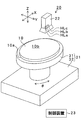
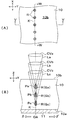
図1は、第1実施形態においてウェハ10にレーザ光を照射して改質領域を形成するためのレーザ加工装置20の概略構成を示す斜視図である。
レーザ加工装置20は、ウェハ載置装置21、レーザ照射装置22、制御装置23などから構成されている。
<First Embodiment>
FIG. 1 is a perspective view showing a schematic configuration of a
The
ウェハ載置装置21は、回転テーブル(ステージ、試料台)31、移動テーブル32などから構成されている。
ウェハ10は円盤形の回転テーブル31上に載置され、ウェハ10の裏面10aは回転テーブル31の上面に吸着固定されている。
回転テーブル31は、移動テーブル32に対して回動可能に軸支され、移動テーブル32内に設けられている駆動装置(図示略)により、ウェハ10の表裏面10b,10aと平行な水平面内にてθ方向に回動される。
移動テーブル32は、レーザ加工装置20の本体ベース(図示略)内に設けられている駆動装置(図示略)により、ウェハ10の表裏面10b,10aと平行な水平面内にてX,Y方向に移動される。
The
The
The rotary table 31 is pivotally supported with respect to the moving table 32, and is driven into a horizontal plane parallel to the front and back surfaces 10b and 10a of the
The moving table 32 is moved in the X and Y directions in a horizontal plane parallel to the front and back surfaces 10 b and 10 a of the
レーザ照射装置22は、回転テーブル31の上方に配置され、レーザ加工装置20に設けられている駆動装置(図示略)により、ウェハ10の表裏面10b,10aと平行な水平面内にてX,Y方向に移動されると共に、ウェハ10の表裏面10b,10aと垂直なZ方向に移動される。
レーザ照射装置22内には3個のレーザヘッドHLa〜HLcが設けられ、各レーザヘッドHLa〜HLcはX方向に並べて配置されている。
The
Three laser heads HLa to HLc are provided in the
制御装置23は、前記各駆動装置を制御することにより、各テーブル31,32およびレーザ照射装置22のX,Y,Z方向の移動を制御する。
尚、X方向とY方向とZ方向はそれぞれ直交する。
The control device 23 controls movement of the tables 31 and 32 and the
The X direction, the Y direction, and the Z direction are orthogonal to each other.
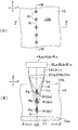
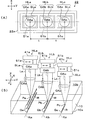
図2(A)は、第1実施形態におけるレーザ照射装置22の底面図である。図2(B)は、第1実施形態におけるレーザ照射装置22の概略構成を説明するための一部縦断面図である。
レーザ照射装置22の筺体22aは底面が開放された箱状を成し、筺体22a内には3個のレーザヘッドHLa〜HLcが取付固定されている。
レーザヘッドHLaはレーザ光源SLaおよび集光レンズCVaを備え、レーザ光源SLaは波長λaのレーザ光Laを出射し、レーザ光Laを集光させた集光点Paの位置は、波長λaと集光レンズCVaの開口数NAaとによって規定される。
レーザヘッドHLbはレーザ光源SLbおよび集光レンズCVbを備え、レーザ光源SLbは波長λbのレーザ光Lbを出射し、レーザ光Lbを集光させた集光点Pbの位置は、波長λbと集光レンズCVaの開口数NAbとによって規定される。
レーザヘッドHLcはレーザ光源SLcおよび集光レンズCVcを備え、レーザ光源SLcは波長λcのレーザ光Lcを出射し、レーザ光Lcを集光させた集光点Pcの位置は、波長λcと集光レンズCVcの開口数NAcとによって規定される。
FIG. 2A is a bottom view of the
The
The laser head HLa includes a laser light source SLa and a condensing lens CVa. The laser light source SLa emits laser light La having a wavelength λa, and the position of the condensing point Pa where the laser light La is condensed is condensing with the wavelength λa. It is defined by the numerical aperture NAa of the lens CVa.
The laser head HLb includes a laser light source SLb and a condensing lens CVb. The laser light source SLb emits a laser beam Lb having a wavelength λb, and the position of a condensing point Pb on which the laser beam Lb is condensed is condensing with the wavelength λb. It is defined by the numerical aperture NAb of the lens CVa.
The laser head HLc includes a laser light source SLc and a condensing lens CVc. The laser light source SLc emits a laser beam Lc having a wavelength λc, and the position of a condensing point Pc where the laser beam Lc is condensed is condensing with the wavelength λc. It is defined by the numerical aperture NAc of the lens CVc.
各レーザ光La〜Lcの光軸OAa〜OAcは、Z方向を向くと共にX方向に並べて配置されている。
制御装置23は、各レーザヘッドHLa〜HLcによる各レーザ光La〜Lcの照射を制御する。
The optical axes OAa to OAc of the laser beams La to Lc are arranged side by side in the Z direction and in the Z direction.
The control device 23 controls irradiation of the laser beams La to Lc by the laser heads HLa to HLc.
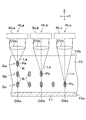
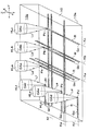
図3および図4は、第1実施形態においてウェハ10にレーザ光La〜Lcを照射して改質領域Rを形成する様子を説明するための説明図であり、図3(A)はウェハ10の平面図を表し、図3(B)および図4はウェハ10の縦断面を模式的に表したものである。
尚、図3(B)は、図3(A)に示すV−V線断面図である。
また、図4は、図3(A)に示す切断予定ラインKに相当するW−W線断面図である。
FIGS. 3 and 4 are explanatory views for explaining a state in which the modified region R is formed by irradiating the
FIG. 3B is a cross-sectional view taken along the line VV shown in FIG.
4 is a cross-sectional view taken along the line WW corresponding to the planned cutting line K shown in FIG.
単結晶シリコンのバルク材から成るウェハ(バルクシリコンウェハ)10の裏面10aには、ダイシングフィルム(ダイシングシート、ダイシングテープ、エキスパンドテープ)11が貼着されている。
尚、ダイシングフィルム11は、加熱により伸張するか又は伸張方向に力を加えることにより伸張する伸張性のプラスチック製フィルム材から成り、ウェハ10の裏面側全面に対して接着剤(図示略)によって接着されている。
A dicing film (dicing sheet, dicing tape, expanded tape) 11 is attached to the
The dicing
ウェハ10の表面10bを上向きにし、ダイシングフィルム11が貼着されているウェハ10の表面10aを下向きにした状態で、ウェハ10を回転テーブル31(図3および図4では図示略。図1参照)上に載置すると、ダイシングフィルム11が回転テーブル31の上面と接触する。
With the
そして、レーザ加工装置20は、各レーザ光La〜Lcの光軸OAa〜OAcをウェハ10の表面10bに対して垂直にすると共に切断予定ラインKに合致させた状態で、各レーザ光La〜Lcを集光レンズCVa〜CVcを介してウェハ10の表面(レーザ光La〜Lcの入射面)10bへ照射させ、ウェハ10の内部における所定位置にレーザ光Lを集光させた異なる集光点(焦点)Pa〜Pcを合わせる。その結果、ウェハ10の内部における異なる集光点Pa〜Pcの箇所にそれぞれ、各レーザ光La〜Lcの照射による改質領域(改質層)Rが形成される。
Then, the
このとき、レーザ光の波長が大きいほど、ウェハ10の内部における集光点の深さ位置が深くなり、ウェハ10の表面10bから深い部分に改質領域Rが形成される。
言い換えれば、レーザ光の波長が大きいほど、レーザ光の入射面(ウェハ10の表面10b)から集光点までの距離が大きくなり、ウェハ10の内部におけるレーザ光の入射面から遠い部分に改質領域Rが形成される。
At this time, as the wavelength of the laser beam increases, the depth position of the condensing point inside the
In other words, the larger the wavelength of the laser light, the greater the distance from the laser light incident surface (the
また、集光レンズの開口数が小さいほど、ウェハ10の内部における集光点の深さ位置が深くなり、ウェハ10の表面10bから深い部分に改質領域Rが形成される。
言い換えれば、集光レンズの開口数が小さいほど、レーザ光の入射面(ウェハ10の表面10b)から集光点までの距離が大きくなり、ウェハ10の内部におけるレーザ光の入射面から遠い部分に改質領域Rが形成される。
ここで、ウェハ10の内部における集光点Pa〜Pcの深さ位置とは、ウェハ10の表面(レーザ光La〜Lcの入射面)10bから集光点Pa〜Pcまでの距離である。
Further, the smaller the numerical aperture of the condensing lens, the deeper the focal position of the condensing point inside the
In other words, the smaller the numerical aperture of the condensing lens, the greater the distance from the laser light incident surface (the
Here, the depth position of the condensing points Pa to Pc in the
そのため、各レーザ光La〜Lcの波長λa〜λcがこの順番で大きくなるように設定しておけば(λa<λb<λc)、各集光点Pa〜Pcの深さ位置をこの順番で深くすることができる。
また、各集光レンズCVa〜CVcの開口数NAa〜NAcがこの順番で小さくなるように設定しておけば(NAa>NAb>NAc)、各集光点Pa〜Pcの深さ位置をこの順番で深くすることができる。
尚、各波長λa〜λcと各開口数NAa〜NAcの両方を前記のように設定しても、各集光点Pa〜Pcの深さ位置をこの順番で深くすることができる。
Therefore, if the wavelengths λa to λc of the laser beams La to Lc are set so as to increase in this order (λa <λb <λc), the depth positions of the condensing points Pa to Pc are increased in this order. can do.
If the numerical apertures NAa to NAc of the condensing lenses CVa to CVc are set so as to decrease in this order (NAa>NAb> NAc), the depth positions of the condensing points Pa to Pc are determined in this order. Can be deep.
Even if both the wavelengths λa to λc and the numerical apertures NAa to NAc are set as described above, the depth positions of the condensing points Pa to Pc can be deepened in this order.
ここで、改質領域Rは、レーザ光La〜Lcの照射によって発生した主に多光子吸収による溶融処理領域を含むものである。
すなわち、ウェハ10の内部における集光点Pa〜Pcの箇所は、レーザ光La〜Lcの多光子吸収によって局所的に加熱され、その加熱により一旦溶融した後に再固化する。このように、ウェハ10の内部にて溶融後に再固化した領域が改質領域Rとなる。
つまり、溶融処理領域とは、相変化した領域や結晶構造が変化した領域である。言い換えれば、溶融処理領域とは、ウェハ10の内部にて、単結晶シリコンが非晶質シリコンに変化した領域、単結晶シリコンが多結晶シリコンに変化した領域、単結晶シリコンが非晶質シリコンおよび多結晶シリコンを含む構造に変化した領域のいずれかの領域である。尚、ウェハ10は、バルクシリコンウェハであるため、溶融処理領域は主に多結晶シリコンから成る。
Here, the modified region R includes a melting treatment region mainly generated by multiphoton absorption generated by the irradiation of the laser beams La to Lc.
That is, the condensing points Pa to Pc inside the
That is, the melt processing region is a region where a phase change or a crystal structure has changed. In other words, the melt processing region is a region where single crystal silicon is changed to amorphous silicon, a region where single crystal silicon is changed to polycrystalline silicon, a single crystal silicon is amorphous silicon, Any of the regions changed to a structure containing polycrystalline silicon. Incidentally, since the
ちなみに、溶融処理領域は、レーザ光La〜Lcがウェハ10の内部で吸収されること(つまり、通常のレーザ光による加熱)によって形成されたものではなく、主に多光子吸収によって形成される。
そのため、ウェハ10の内部における集光点Pa〜Pcの箇所以外にはレーザ光La〜Lcがほとんど吸収されず、ウェハ10の表面10bが溶融したり変質することはない。
Incidentally, the melt processing region is not formed by the laser beams La to Lc being absorbed inside the wafer 10 (that is, heating by a normal laser beam), but is mainly formed by multiphoton absorption.
Therefore, the laser beams La to Lc are hardly absorbed except for the condensing points Pa to Pc inside the
そして、レーザ加工装置20は、ウェハ10の内部における各集光点Pa〜Pcの深さ位置を一定にした状態で、レーザ照射装置22をX方向に移動させ、各レーザ光La〜Lcをパルス状に照射しながら走査することにより、ウェハ10における直線状の切断予定ラインKに沿ってX方向に集光点Pa〜Pcを移動させる。
Then, the
ところで、レーザ照射装置22を移動させることによって各レーザ光La〜Lcを走査するのではなく、レーザ照射装置22を固定した状態で、各テーブル31,32を各レーザ光La〜Lcの照射方向(ウェハ10の表面10bに対するレーザ光La〜Lcの入射方向)と直交する方向に回動または移動させてもよい。
すなわち、レーザ照射装置22を移動させることによるレーザ光La〜Lcの走査と、各テーブル31,32を回動・移動させることによるウェハ10の移動により、ウェハ10の切断予定ラインKに沿いながら、ウェハ10に対して各集光点Pa〜Pcを相対的に移動させればよい。
By the way, instead of scanning each laser beam La to Lc by moving the
That is, along the planned cutting line K of the
このように、ウェハ10の内部における各集光点Pa〜Pcの深さ位置を一定にした状態で、各レーザ光La〜Lcをパルス状に照射しながら、ウェハ10に対して各集光点Pa〜Pcを相対的に移動させることにより、ウェハ10の表面10bから一定深さ位置にて(つまり、レーザ光La〜Lcの入射面から一定距離内側の位置にて)、ウェハ10の表裏面10b,10aに対して水平方向(X方向)に一定の間隔をあけた複数個の改質領域Rから成る3層1組の改質領域群Ga〜Gcが同時に形成されてゆく。
In this way, each of the condensing points is applied to the
このとき、3層の改質領域群Gc〜Gaを構成する各改質領域Rは、レーザ光La〜Lcが入射するウェハ10の表面(レーザ光Lの入射面)10bに対して遠い方から順番に(Gc→Gb→Gaの順番で)形成する必要がある。
例えば、レーザ光Lが入射するウェハ10の表面10bに対して近い位置の改質領域群Gaを先に形成し、その後にレーザ光Lが入射するウェハ10の表面10bに対して遠い位置の改質領域群Gcを形成した場合には、改質領域群Gcの形成時に照射されたレーザ光Lが先に形成された改質領域群Gaによって散乱されるため、改質領域群Gcを構成する各改質領域Rの寸法にバラツキが生じ、改質領域群Gcを均一に形成することができない。
At this time, each modified region R constituting the three-layered modified region group Gc to Ga is from a position far from the surface (incident surface of the laser beam L) 10b of the
For example, the modified region group Ga at a position close to the
しかし、レーザ光Lが入射するウェハ10の表面(レーザ光Lの入射面)10bに対して遠い方から順番に改質領域群Gc〜Gaを形成すれば、当該入射面10bと集光点Pとの間に改質領域Rがない状態で新たな改質領域Rを形成可能なため、既に形成されている改質領域Rによってレーザ光Lが散乱されず、3層の改質領域群Ga〜Gcをそれぞれ均一に形成することができる。
However, if the modified region groups Gc to Ga are formed in order from the far side with respect to the
従って、図4に示すように、各集光点Pa〜Pcを切断予定ラインKに沿って相対的に移動させる際に、集光点Pcを先頭にし集光点Pbが続いて集光点Paが最後になって各集光点Pc〜Paがこの順番(Pc→Pb→Pa)で移動される場合には、各集光点Pc〜Paの深さ位置がこの順番で浅くなるように設定しなければならない。
すなわち、集光点Pcの深さ位置が最も深く、集光点Paの深さ位置が最も浅く、集光点Pbの深さ位置が各集光点Pa,Pcの深さ位置の中間になるように設定しなければならない。
Therefore, as shown in FIG. 4, when each of the condensing points Pa to Pc is relatively moved along the scheduled cutting line K, the condensing point Pb follows the condensing point Pc, followed by the condensing point Pa. When the condensing points Pc to Pa are moved in this order (Pc → Pb → Pa), the depth positions of the condensing points Pc to Pa are set so as to become shallower in this order. Must.
That is, the depth position of the condensing point Pc is the deepest, the depth position of the condensing point Pa is the shallowest, and the depth position of the condensing point Pb is in the middle of the depth positions of the respective condensing points Pa and Pc. Must be set to
このようにすれば、集光点Paによって形成される改質領域群Gaを最上層にし、集光点Pbによって形成される改質領域群Gbを中間層にし、集光点Pcによって形成される改質領域群Gaを最下層にした上で、レーザ光La〜Lcが入射するウェハ10の表面(レーザ光Lの入射面)10bに対して遠い方から順番(Gc→Gb→Ga)に各改質領域群Gc〜Gaを構成する各改質領域Rを形成することができる。
In this way, the modified region group Ga formed by the condensing point Pa is the uppermost layer, the modified region group Gb formed by the condensing point Pb is the intermediate layer, and the condensing point Pc is formed. With the modified region group Ga as the lowest layer, the laser beam La to Lc is incident on each of the
以上のように、ウェハ10の内部に各改質領域群Ga〜Gcを形成した後に、ダイシングフィルム11を切断予定ラインに対して水平方向(図3に示す矢印β,β’方向。つまり、Y方向)に伸張させることにより、各改質領域群Ga〜Gcに引張応力を印加する。
As described above, after the respective modified region groups Ga to Gc are formed inside the
すると、ウェハ10の内部に剪断応力が発生し、まず、ダイシングフィルム11に最も近い最下層の改質領域群Gcを起点としてウェハ10の深さ方向に亀裂(割れ)が発生し、次に、中間層の改質領域群Gbを起点としてウェハ10の深さ方向に亀裂が発生し、続いて、最上層の改質領域群Gaを起点としてウェハ10の深さ方向に亀裂が発生し、各改質領域群Ga〜Gcを起点とした亀裂がそれぞれ成長して繋がり、その成長した亀裂がウェハ10の表裏面10b,10aに到達することにより、ウェハ10が切断分離される。
Then, a shear stress is generated inside the
ここで、各改質領域群Ga〜Gcは切断予定ラインKに沿って形成されているため、ダイシングフィルム11を伸張させて各改質領域群Ga〜Gcに引張応力を好適に印加させることで、各改質領域群Ga〜Gcを構成する各改質領域Rを切断の起点とした割断により、ウェハ10に不要な割れを生じさせることなく、ウェハ10を比較的小さな力で精度良く切断分離することができる。
Here, since each modified region group Ga to Gc is formed along the planned cutting line K, the dicing
尚、薄板略円板状のウェハ10の表面10bには、多数個のチップ(図示略)が碁盤目状に整列配置されており、切断予定ラインKは各チップの間に配置されている。つまり、ウェハ10の表面10bには複数本の切断予定ラインKが格子状に配置されている。
そのため、各改質領域群Ga〜Gcを各切断予定ラインK毎に形成した後に、ダイシングフィルム11を伸張させることにより、ウェハ10を個々のチップに切断分離することができる。
Note that a large number of chips (not shown) are arranged in a grid pattern on the
Therefore, the
[第1実施形態の作用・効果]
第1実施形態では、各レーザ光La〜Lcをそれぞれ出射する3個のレーザヘッドHLa〜HLcを用いている。
そして、各レーザ光La〜Lcの波長λa〜λcまたは集光レンズCVa〜CVcの開口数NAa〜NAcの少なくともいずれか一方を調整することにより、ウェハ10の内部における各レーザ光La〜Lcの集光点Pa〜Pcの深さ位置を適宜設定し、ウェハ10の切断予定ラインKに沿うと共に、ウェハ10の表面10bから深さ方向に離間または隣接または重複して配置された3層1組の改質領域群Ga〜Gcを構成する各改質領域Rを同時に形成している。
[Operations and effects of the first embodiment]
In the first embodiment, three laser heads HLa to HLc that respectively emit laser beams La to Lc are used.
Then, by adjusting at least one of the wavelengths λa to λc of the laser beams La to Lc and the numerical apertures NAa to NAc of the condenser lenses CVa to CVc, the collection of the laser beams La to Lc in the
言い換えれば、ウェハ10に照射されるレーザ光La〜Lcのウェハ10への入射方向(ウェハ10の深さ方向)におけるレーザ光La〜Lcの集光点Pa〜Pcを異なる位置(深さ位置)に設定することにより、3組6層の改質領域群Ga〜Gcを構成する各改質領域Rを前記入射方向に沿って離間または隣接または重複させた状態で並ぶように複数形成している。
In other words, the condensing points Pa to Pc of the laser beams La to Lc in the incident direction (depth direction of the wafer 10) of the laser beams La to Lc irradiated to the
このように、第1実施形態では、各レーザ光La〜Lcを同時にウェハ10に照射することにより、各レーザ光La〜Lcにそれぞれ対応した深さの異なる3層の改質領域群Ga〜Gcを構成する各改質領域Rを形成している。
そのため、第1実施形態によれば、ウェハの表面から深さ方向に1層の改質領域しか形成しない特許文献1の技術に比べて、ウェハ10の板厚が大きい場合でも、ウェハ10を切断する際に起点となる改質領域Rの個数が増すことから、切断予定ラインKに沿って精度良く切断分離することができる。
As described above, in the first embodiment, by irradiating the
Therefore, according to the first embodiment, the
そして、第1実施形態では、各改質領域群Ga〜Gcを同時に形成しているため加工効率が高くなり、短時間に3層の正常な改質領域群Ga〜Gcを確実に形成可能であるため、スループットが高く量産化に好適である。 In the first embodiment, the modified region groups Ga to Gc are simultaneously formed, so that the processing efficiency is increased, and the three layers of the modified region groups Ga to Gc can be reliably formed in a short time. Therefore, it has a high throughput and is suitable for mass production.
また、第1実施形態では、ウェハ10の表面10bに対して各レーザ光La〜Lcを垂直方向に入射しているため、各レーザ光La〜Lcが照射される切断予定ラインKの幅を狭くすることが可能になり、1枚のウェハ10から切り取ることが可能なチップの個数が、切断予定ラインKの幅を広くした場合に比べて多くなることから、チップの製造コストを削減できる。
In the first embodiment, since the laser beams La to Lc are incident on the
さらに、第1実施形態では、ウェハ10の表面(レーザ光Lの入射面)10bに対して遠い方から順番に各改質領域群Gc〜Gaを構成する各改質領域Rが形成されるように、ウェハ10に対する各集光点Pa〜Pcの移動方向を設定すると共に、各集光点Pa〜Pcの深さ位置を設定している。
そのため、ウェハ10の表面10bから浅い部分に形成された改質領域Rが、深い部分に改質領域Rを形成する際のレーザ光の入射を阻害することなく、当該深い部分にも正常な改質領域Rを確実に形成することができる。
Furthermore, in the first embodiment, the respective modified regions R constituting the respective modified region groups Gc to Ga are formed in order from the far side from the surface (incident surface of the laser beam L) 10b of the
Therefore, the modified region R formed in the shallow portion from the
尚、第1実施形態では3個のレーザヘッドHLa〜HLcを用いて3層の改質領域群Ga〜Gcを形成しているが、2個または4個以上のレーザヘッドを用いて2層または4層以上の改質領域群を形成するようにしてもよい。 In the first embodiment, the three modified region groups Ga to Gc are formed using three laser heads HLa to HLc, but two or four or more laser heads are used to form two layers or Four or more modified region groups may be formed.
<第2実施形態>
図5(A)は、第2実施形態におけるレーザ照射装置22の底面図である。図5(B)は、第2実施形態におけるレーザ照射装置22の概略構成を説明するための一部縦断面図である。
Second Embodiment
FIG. 5A is a bottom view of the
図6および図7は、第2実施形態においてウェハ10にレーザ光La〜Lcを照射して改質領域Rを形成する様子を説明するための説明図であり、図6(A)はウェハ10の平面図を表し、図6(B)および図7はウェハ10の縦断面を模式的に表したものである。
尚、図6(B)は、図6(A)に示すV−V線断面図である。
また、図7は、図6(A)に示す切断予定ラインKに相当するW−W線断面図である。
FIG. 6 and FIG. 7 are explanatory views for explaining a state in which the modified region R is formed by irradiating the
Note that FIG. 6B is a cross-sectional view taken along line VV shown in FIG.
FIG. 7 is a cross-sectional view taken along the line WW corresponding to the planned cutting line K shown in FIG.
第2実施形態において、第1実施形態と異なるのは、以下の点だけである。
[2−1]レーザ照射装置22内には3個の駆動装置41a〜41cが設けられている。
[2−2]駆動装置41aは、レーザヘッドHLaを光軸OAaに沿った方向であるZ方向に進退移動させる。駆動装置41bは、レーザヘッドHLbを光軸OAbに沿った方向であるZ方向に進退移動させる。駆動装置41cは、レーザヘッドHLcを光軸OAcに沿った方向であるZ方向に進退移動させる。尚、各駆動装置41a〜41cは、どのような機構(例えば、ラック・ピニオン、ボールねじなど)によって具体化してもよい。
[2−3]制御装置23は、各駆動装置41a〜41cを制御することにより、各レーザヘッドHLa〜HLcのZ方向の移動を制御する。
[2−4]各レーザ光La〜Lcの波長および集光レンズCVa〜CVcの開口数はそれぞれ同じ値に設定されている。
The second embodiment differs from the first embodiment only in the following points.
[2-1] Three
[2-2] The
[2-3] The control device 23 controls movement of the laser heads HLa to HLc in the Z direction by controlling the
[2-4] The wavelengths of the laser beams La to Lc and the numerical apertures of the condenser lenses CVa to CVc are set to the same value.
このように、第2実施形態では、各駆動装置41a〜41cを用いて各レーザヘッドHLa〜HLcのZ方向の位置を調整することにより、第1実施形態と同様に、ウェハ10の内部における各レーザ光La〜Lcの集光点Pa〜Pcの深さ位置を適宜設定し、ウェハ10の切断予定ラインKに沿うと共に、ウェハ10の表面10bから深さ方向に離間または隣接または重複して配置された3層1組の改質領域群Ga〜Gcを同時に形成している。
従って、第2実施形態によれば、第1実施形態と同様の作用・効果を得ることができる。
As described above, in the second embodiment, the positions of the laser heads HLa to HLc in the Z direction are adjusted by using the
Therefore, according to the second embodiment, the same operation and effect as the first embodiment can be obtained.
<第3実施形態>
図8(A)は、第3実施形態におけるレーザ照射装置22の底面図である。
図8(B)は、第3実施形態においてウェハ10にレーザ光La〜Lcを照射して改質領域Rを形成する様子を説明するための説明図であり、ウェハ10の一部透視斜視図である。
<Third Embodiment>
FIG. 8A is a bottom view of the
FIG. 8B is an explanatory view for explaining a state in which the modified region R is formed by irradiating the
第3実施形態において、第1実施形態と異なるのは、以下の点だけである。
[3−1]レーザ照射装置22内に設けられた各レーザヘッドHLa〜HLcから照射される各レーザ光La〜Lcの光軸OAa〜OAcは、Z方向を向くと共にY方向に並べて配置されている。
[3−2]レーザ照射装置22内には3個の駆動装置51a〜51cが設けられている。
[3−3]各駆動装置51a〜51cはそれぞれ、各レーザヘッドHLa〜HLcをY方向に進退移動させる。尚、各駆動装置51a〜51cは、どのような機構(例えば、ラック・ピニオン、ボールねじなど)によって具体化してもよい。
The third embodiment is different from the first embodiment only in the following points.
[3-1] The optical axes OAa to OAc of the laser beams La to Lc irradiated from the laser heads HLa to HLc provided in the
[3-2] Three
[3-3] Each of the
[3−4]制御装置23は、各駆動装置51a〜51cを制御することにより、各レーザヘッドHLa〜HLcのY方向の移動を制御し、各光軸OAa〜OAcの間隔tをウェハ10に配置された平行な切断予定ラインKa〜Kcの間隔に設定する。
前記のように、切断予定ラインはウェハ10から切断分離される各チップの間に配置されているため、切断予定ラインKa〜Kcの間隔(光軸OAa〜OAcの間隔t)が1個のチップの幅または奥行の寸法となる。
また、各切断予定ラインKa〜KcはX方向に沿うと共にY方向に並べて配置されているため、各レーザヘッドHLa〜HLcが進退移動されるY方向は、各切断予定ラインKa〜Kcと直交する水平方向になる。
[3-4] The control device 23 controls the movement of the laser heads HLa to HLc in the Y direction by controlling the
As described above, since the scheduled cutting line is arranged between the chips that are cut and separated from the
In addition, since each of the planned cutting lines Ka to Kc is arranged along the X direction and in the Y direction, the Y direction in which the laser heads HLa to HLc are moved back and forth is orthogonal to the planned cutting lines Ka to Kc. Become horizontal.
[3−5]レーザ加工装置20は、各レーザ光La〜Lcの光軸OAa〜OAcをウェハ10の表面10bに対して垂直にすると共に、各光軸OAa〜OAcをそれぞれ各切断予定ラインKa〜Kcに合致させた状態で、各レーザ光La〜Lcを集光レンズCVa〜CVcを介してウェハ10の表面10bへ照射させ、ウェハ10の内部における所定位置にレーザ光Lを集光させた各集光点Pa〜Pcを合わせ、各集光点Pa〜Pcの箇所に各レーザ光La〜Lcの照射による改質領域Rを形成する。
[3-5] The
そして、レーザ加工装置20は、ウェハ10の内部における各集光点Pa〜Pcの深さ位置を一定にした状態で、各レーザ光La〜Lcをパルス状に照射しながら、ウェハ10に対して各集光点Pa〜Pcを相対的にX方向へ移動させることにより、各切断予定ラインKa〜Kcに沿ってX方向に一定の間隔をあけた複数個の改質領域Rから成る3本の改質領域群Ga〜Gcを同時に形成されてゆく。
ここで、レーザ加工装置20は、第1実施形態と同様に、各レーザ光La〜Lcの波長λa〜λcまたは集光レンズCVa〜CVcの開口数NAa〜NAcの少なくともいずれか一方を調整することにより、各集光点Pa〜Pcの深さ位置を設定する。
Then, the
Here, as in the first embodiment, the
[3−6]レーザ加工装置20は、ウェハ10の内部における集光点Pa〜Pcの深さ位置を段階的に変えることにより、各切断予定ラインKa〜Kcに沿うと共に、ウェハ10の表面10bから深さ方向(ウェハ10の厚さ方向、ウェハ10の断面方向、ウェハ10の表裏面10b,10aに対して垂直方向)に離間または隣接または重複して配置された複数層の改質領域群を構成する各改質領域Rを順次形成する。
[3-6] The
図8(B)に示す例では、切断予定ラインKaに沿って3層の改質領域群Gaが形成され、切断予定ラインKbに沿って2層の改質領域群Gbが形成され、切断予定ラインKcに沿って1層の改質領域群Gaが形成されている。 In the example shown in FIG. 8B, a three-layer modified region group Ga is formed along the planned cutting line Ka, and a two-layer modified region group Gb is formed along the planned cutting line Kb. A single modified region group Ga is formed along the line Kc.
このとき、第1実施形態と同様に、ウェハ10におけるレーザ入射面である表面10bから遠い位置(すなわち深い位置)の改質領域Rが必ず先に形成されるように、ウェハ10に対する各集光点Pa〜Pcの移動方向を設定すると共に、各集光点Pa〜Pcの深さ位置を設定しておく。
At this time, in the same manner as in the first embodiment, each light condensing with respect to the
このように、第3実施形態では、各駆動装置51a〜51cを用いて各レーザヘッドHLa〜HLcのY方向の位置を調整することにより、各光軸OAa〜OAcの間隔tをウェハ10の切断予定ラインKa〜Kcの間隔に設定し、各レーザ光La〜Lcの集光点Pa〜Pcの深さ位置を第1実施形態と同様に設定した状態で、各集光点Pa〜Pcを切断予定ラインKa〜Kcに沿ってX方向に移動している。
As described above, in the third embodiment, by adjusting the positions of the laser heads HLa to HLc in the Y direction using the
従って、第3実施形態によれば、各切断予定ラインKa〜Kcに沿った3本の改質領域群Ga〜Gcを同時に形成することが可能になるため加工効率を高くできる。
尚、第3実施形態では3個のレーザヘッドHLa〜HLcを用いて3本の改質領域群Ga〜Gcを形成しているが、2個または4個以上のレーザヘッドを用いて2本または4本以上の改質領域群を形成するようにしてもよい。
Therefore, according to the third embodiment, the three modified region groups Ga to Gc along the scheduled cutting lines Ka to Kc can be simultaneously formed, so that the processing efficiency can be increased.
In the third embodiment, three modified region groups Ga to Gc are formed using three laser heads HLa to HLc, but two or four or more laser heads are used to form two or Four or more modified region groups may be formed.
また、第3実施形態では、第1実施形態と同様に、ウェハ10の表面10bに対して各レーザ光La〜Lcを垂直方向に入射しているため、各レーザ光La〜Lcが照射される切断予定ラインKの幅を狭くすることが可能になり、1枚のウェハ10から切り取ることが可能なチップの個数が、切断予定ラインKの幅を広くした場合に比べて多くなることから、チップの製造コストを削減できる。
In the third embodiment, similarly to the first embodiment, the laser beams La to Lc are incident on the
さらに、第3実施形態では、第1実施形態と同様に、ウェハ10の表面(レーザ光Lの入射面)10bに対して遠い方から順番に各改質領域群Gc〜Gaを構成する各改質領域Rが形成されるように、ウェハ10に対する各集光点Pa〜Pcの移動方向を設定すると共に、各集光点Pa〜Pcの深さ位置を設定している。
そのため、ウェハ10の表面10bから浅い部分に形成された改質領域Rが、深い部分に改質領域Rを形成する際のレーザ光の入射を阻害することなく、当該深い部分にも正常な改質領域Rを確実に形成することができる。
Furthermore, in the third embodiment, as in the first embodiment, each modified region group Gc to Ga constituting each modified region group Gc to Ga in order from the far side with respect to the surface (incident surface of the laser beam L) 10b of the
Therefore, the modified region R formed in the shallow portion from the
<第4実施形態>
図9(A)は、第4実施形態におけるレーザ照射装置22の底面図である。
図9(B)は、第4実施形態においてウェハ10にレーザ光La〜Lcを照射して改質領域Rを形成する様子を説明するための説明図であり、ウェハ10の一部透視斜視図である。
<Fourth embodiment>
FIG. 9A is a bottom view of the
FIG. 9B is an explanatory diagram for explaining a state in which the modified region R is formed by irradiating the
第4実施形態において、第3実施形態と異なるのは、第2実施形態の前記[2−1]〜[2−4]と同じ構成が設けられており、各駆動装置41a〜41cを用いて各レーザヘッドHLa〜HLcのZ方向の位置を調整することにより、ウェハ10の内部における各レーザ光La〜Lcの集光点Pa〜Pcの深さ位置を設定している点だけである。
従って、第4実施形態によれば、第3実施形態と同様の作用・効果を得ることができる。
In the fourth embodiment, the difference from the third embodiment is that the same configuration as [2-1] to [2-4] in the second embodiment is provided, and the
Therefore, according to the fourth embodiment, the same operation and effect as the third embodiment can be obtained.
<第5実施形態>
図10は、第5実施形態においてウェハ10にレーザ光Ld〜Lgを照射して改質領域Rを形成する様子を説明するための説明図であり、ウェハ10の一部透視斜視図である。
<Fifth Embodiment>
FIG. 10 is an explanatory view for explaining a state in which the modified region R is formed by irradiating the
第5実施形態において、第3実施形態または第4実施形態と異なるのは、以下の点だけである。
[5−1]3個1組のレーザヘッドHLa〜HLcと同様の構成の3個1組のレーザヘッドHLd〜HLfが設けられている。
[5−2]第3実施形態または第4実施形態と同様に、各レーザヘッドHLa〜HLcから照射される各レーザ光La〜Lcの光軸OAa〜OAcをZ方向に向け、各集光点Pa〜Pcをウェハ10に対して相対的にX方向に移動し、ウェハ10に配置された平行な切断予定ラインKa〜Kcに沿って、3本の改質領域群Ga〜Gcを構成する各改質領域Rを形成する。
また、各レーザヘッドHLd〜HLfから照射される各レーザ光Ld〜Lfの光軸OAd〜OAfをZ方向に向け、各集光点Pd〜Pfをウェハ10に対して相対的にY方向に移動し、ウェハ10に配置された平行な切断予定ラインKd〜Kfに沿って、3本の改質領域群Gd〜Gfを構成する各改質領域Rを形成する。
尚、各切断予定ラインKa〜KcはX方向に沿って配置され、各切断予定ラインKd〜KfはY方向に沿って配置され、各切断予定ラインKa〜Kfは格子状に配置されている。
The fifth embodiment differs from the third embodiment or the fourth embodiment only in the following points.
[5-1] A set of three laser heads HLd to HLf having the same configuration as the set of three laser heads HLa to HLc is provided.
[5-2] Similar to the third embodiment or the fourth embodiment, the optical axes OAa to OAc of the laser beams La to Lc irradiated from the laser heads HLa to HLc are directed in the Z direction, and the respective condensing points. Pa to Pc are moved relative to the
Further, the optical axes OAd to OAf of the laser beams Ld to Lf irradiated from the laser heads HLd to HLf are directed in the Z direction, and the respective condensing points Pd to Pf are moved relative to the
Each of the planned cutting lines Ka to Kc is arranged along the X direction, each of the planned cutting lines Kd to Kf is arranged along the Y direction, and each of the planned cutting lines Ka to Kf is arranged in a grid pattern.
このように、第5実施形態では、3個1組のレーザヘッドHLa〜HLc,HLd〜HLfを2組備え、その2組のレーザヘッドから同時に照射された6つのレーザ光La〜Lfをパルス状に照射しながら、各レーザ光La〜Lfの集光点Pa〜Pfをウェハ10の表裏面10b,10aに対して水平方向に直交する2方向(X,Y方向)に移動させることにより、ウェハ10に対して格子状に配置された6本の切断予定ラインKa〜Kfに沿った複数個の改質領域Rから成る6本の改質領域群Ga〜Gfを同時に形成している。
As described above, in the fifth embodiment, two sets of three laser heads HLa to HLc and HLd to HLf are provided, and the six laser beams La to Lf irradiated simultaneously from the two sets of laser heads are pulsed. By moving the condensing points Pa to Pf of the laser beams La to Lf in two directions (X and Y directions) perpendicular to the horizontal direction with respect to the front and back surfaces 10b and 10a of the
従って、第5実施形態によれば、X方向とY方向の両方向にそれぞれ3本ずつの改質領域群を構成する各改質領域Rを同時に形成可能になるため、第3実施形態または第4実施形態よりも更に加工効率を高くできる。
尚、第5実施形態では3個1組のレーザヘッドHLa〜HLc,HLd〜HLfを2組用いて6本の改質領域群Ga〜Gfを形成しているが、2個1組または4個以上を1組とするレーザヘッドを3組以上用いることにより、複数本の改質領域群を形成するようにしてもよい。
Therefore, according to the fifth embodiment, each of the modified regions R constituting three modified region groups can be simultaneously formed in both the X direction and the Y direction. The processing efficiency can be further increased as compared with the embodiment.
In the fifth embodiment, six groups of modified regions Ga to Gf are formed by using two sets of three laser heads HLa to HLc and HLd to HLf. A plurality of modified region groups may be formed by using three or more sets of laser heads with one set as described above.
<第6実施形態>
図11(A)(B)は、第6実施形態におけるレーザ照射装置22の底面図である。
第6実施形態において、第3実施形態または第4実施形態と異なるのは、レーザ照射装置22内に設けられた各レーザヘッドHLa〜HLcが、少なくとも各レーザヘッドHLa〜HLcのX方向の幅分だけ、X方向にずらして配置されている点だけである。
<Sixth Embodiment>
11A and 11B are bottom views of the
The sixth embodiment differs from the third embodiment or the fourth embodiment in that the laser heads HLa to HLc provided in the
従って、第6実施形態によれば、各駆動装置51a〜51cを用いて各レーザヘッドHLa〜HLcのY方向の位置を調整することにより、各光軸OAa〜OAcの間隔tの最小値をゼロにまですることが可能であり、当該間隔tを第3実施形態または第4実施形態に比べて小さく設定できることから、ウェハ10から切断分離されるチップのサイズが小さな場合にも容易に対応することができる。
Therefore, according to the sixth embodiment, the minimum value of the interval t between the optical axes OAa to OAc is set to zero by adjusting the positions of the laser heads HLa to HLc in the Y direction using the
<別の実施形態>
本発明は上記各実施形態に限定されるものではなく、以下のように具体化してもよく、その場合でも、上記各実施形態と同等もしくはそれ以上の作用・効果を得ることができる。
<Another embodiment>
The present invention is not limited to the above-described embodiments, and may be embodied as follows. Even in this case, operations and effects equivalent to or higher than those of the above-described embodiments can be obtained.
[1]上記実施形態はバルクシリコンウェハに適用したものであるが、本発明の適用はこれに限られるものではなく、多層構造の半導体基板を作成するための半導体材料から成るウェハに適用してもよい。
その場合、ウェハとしては、例えば、貼り合わせSOI(Silicon On Insulator)構造のウェハ、SIMOX(Separation by IMplanted OXygen)構造のウェハ、ガラスなどの絶縁基板上に多結晶シリコンまたは非晶質シリコンを固相成長法や溶融再結晶化法により形成したSOI構造のウェハ、サファイアなどの基板上にIII−V族化合物半導体層を結晶成長させた半導体発光素子に用いられるウェハ、陽極接合を用いてシリコン基板とガラス基板とを貼り合わせて形成したウェハなどがある。
[1] Although the above embodiment is applied to a bulk silicon wafer, the application of the present invention is not limited to this, and is applied to a wafer made of a semiconductor material for producing a semiconductor substrate having a multilayer structure. Also good.
In that case, for example, a bonded SOI (Silicon On Insulator) structure wafer, a SIMOX (Separation by IMplanted OXygen) structure wafer, a polycrystalline silicon or amorphous silicon solid phase on an insulating substrate such as glass is used. An SOI structure wafer formed by a growth method or a melt recrystallization method, a wafer used for a semiconductor light emitting device in which a III-V compound semiconductor layer is crystal-grown on a substrate such as sapphire, and a silicon substrate using anodic bonding There is a wafer formed by bonding a glass substrate.
その場合、1台のレーザ加工装置20に複数のレーザヘッドHLa〜HLfを設けてあるため、異なる材質のウェハを複数枚積層させた多層構造のウェハに対して、各レーザヘッドHLa〜HLfから照射するレーザ光La〜Lfの波長および開口数を多層構造の各層の材質に対応した最適なものに設定しておけば、各層に最適なレーザ光を照射することが可能になることから、各層毎に正常な改質領域Rを確実に成形することができる。
In that case, since a plurality of laser heads HLa to HLf are provided in one
従来、異なる材質のウェハを複数枚積層させた多層構造のウェハの各層に対して改質領域Rを形成するには、多層構造の各層の材質に対応したレーザ光を照射するレーザヘッドを備えたレーザ加工装置を各層毎に用意しておき、1つの層に改質領域Rを形成する度に別のレーザ加工装置にウェハを移し替える必要があった。
しかし、上記各実施形態を多層構造のウェハのレーザ加工に適用すれば、1台のレーザ加工装置20を用いるだけで、多層構造の各層の材質に対応した最適なレーザ光を照射可能であることから、別のレーザ加工装置にウェハを移し替えることなく、各層に同時もしくは連続して改質領域Rを形成可能なため、加工効率が向上すると共に、複数のレーザ加工装置を設置した場合に比べて装置の設置スペースを削減できる。
Conventionally, in order to form the modified region R for each layer of a wafer having a multilayer structure in which a plurality of wafers of different materials are laminated, a laser head that irradiates laser light corresponding to the material of each layer of the multilayer structure has been provided. A laser processing apparatus is prepared for each layer, and it is necessary to transfer the wafer to another laser processing apparatus each time the modified region R is formed in one layer.
However, if each of the above embodiments is applied to laser processing of a wafer having a multilayer structure, it is possible to irradiate an optimum laser beam corresponding to the material of each layer of the multilayer structure by using only one
[2]上記実施形態はバルクシリコンウェハに適用したものであるが、本発明の適用はこれに限られるものではなく、半導体基板(例えば、ガリウム砒素基板など)を作成するための半導体材料(例えば、ガリウム砒素など)から成るウェハであれば、どのようなウェハに適用してもよい。
また、本発明は、半導体基板を作成するための半導体材料から成るウェハに限らず、種々の材料(例えば、ガラスを含む材料など)から成るウェハに適用してもよい。
[2] Although the above embodiment is applied to a bulk silicon wafer, the application of the present invention is not limited to this, and a semiconductor material (for example, a gallium arsenide substrate) for producing a semiconductor substrate (for example, a gallium arsenide substrate) is used. As long as the wafer is made of gallium arsenide or the like, any wafer may be used.
The present invention is not limited to a wafer made of a semiconductor material for forming a semiconductor substrate, but may be applied to a wafer made of various materials (for example, a material containing glass).
その場合、多光子吸収による改質領域Rは、上記各実施形態のような溶融処理領域を含むものに限らず、ウェハの形成材料に合わせた適宜なものにすればよい。例えば、ウェハの形成材料がガラスを含む場合には、多光子吸収による改質領域Rを、クラック領域を含むものか又は屈折率が変化した領域を含むものにすればよい。
尚、クラック領域または屈折率が変化した領域を含む改質領域については、特許文献1に開示されているため、説明を省略する。
In this case, the modified region R by multiphoton absorption is not limited to the one including the melt processing region as in each of the above embodiments, and may be an appropriate one according to the wafer forming material. For example, when the wafer forming material includes glass, the modified region R by multiphoton absorption may include a crack region or a region having a changed refractive index.
Note that the modified region including the crack region or the region where the refractive index has changed is disclosed in
[3]上記実施形態では、ダイシングフィルム11を伸張させることによりウェハ10を切断分離している。しかし、曲率を有した物(例えば、半球状の物)の曲面(膨らんだ方の面)をウェハ10の切断予定ラインに押し当てて押圧力を印加することにより、改質領域Rに剪断応力を発生させ、ウェハ10を切断分離するようにしてもよい。
[3] In the above embodiment, the
10…ウェハ
10a…ウェハ10の裏面
10b…ウェハ10の表面
11…ダイシングフィルム
20…レーザ加工装置
21…ウェハ載置装置
22…レーザ照射装置
23…制御装置(垂直移動手段、水平移動手段)
31…回転テーブル
32…移動テーブル
41a〜41c…駆動装置(垂直移動手段)
51a〜51c…駆動装置(水平移動手段)
HLa〜HLf…レーザヘッド
La〜Lf…レーザ光
CVa〜CVc…集光レンズ
Pa〜Pf…集光点
OAa〜OAc光軸
R…改質領域
Ga〜Gf…改質領域群
K…切断予定ライン
DESCRIPTION OF
DESCRIPTION OF
51a-51c ... Driving device (horizontal movement means)
HLa to HLf ... Laser head La to Lf ... Laser light CVa to CVc ... Condensing lens Pa to Pf ... Condensing point OAa to OAc optical axis R ... Modified region Ga to Gf ... Modified region group K ... Scheduled cutting line
Claims (10)
レーザ光を発生させて出射するレーザ光源と、そのレーザ光源の出射したレーザ光を前記集光点に集光させる集光レンズとを有する複数個のレーザヘッドを備え、
前記複数個のレーザヘッドから同時に照射された複数のレーザ光をそれぞれ異なる集光点に合わせ、ウェハの表面から深さ方向に間隔をあけた複数層の改質領域を同時に形成することと、
ウェハの切断予定ラインに沿って、前記複数のレーザ光をパルス状に照射しながら、前記ウェハに対して前記複数の集光点を相対的に移動させることにより、前記ウェハの表裏面に対して水平方向に間隔をあけて形成された複数個の改質領域から成る複数層の改質領域群を同時に形成することと、
前記複数のレーザ光をウェハの表面に対して垂直方向に入射させることと、
ウェハの表面から深い位置の改質領域が必ず先に形成されるように、ウェハに対する前記複数の集光点の移動方向を設定すると共に、前記複数の集光点のウェハの内部における深さ位置を設定することと
を特徴とするレーザ加工装置。 A laser processing apparatus that forms a modified region by multiphoton absorption inside a wafer by irradiating a laser beam with a focusing point inside the wafer,
A plurality of laser heads having a laser light source that generates and emits laser light, and a condensing lens that condenses the laser light emitted from the laser light source at the condensing point;
A plurality of laser beams simultaneously irradiated from the plurality of laser heads are respectively aligned with different condensing points, and simultaneously formed a plurality of modified regions spaced in the depth direction from the surface of the wafer;
By moving the plurality of condensing points relative to the wafer while irradiating the plurality of laser beams in a pulsed manner along the wafer cutting schedule line, Simultaneously forming a plurality of modified region groups consisting of a plurality of modified regions formed at intervals in the horizontal direction;
Making the plurality of laser beams incident in a direction perpendicular to the surface of the wafer;
The moving direction of the plurality of condensing points with respect to the wafer is set so that a modified region at a deep position from the wafer surface is always formed first, and the depth positions inside the wafer of the plurality of condensing points are set. A laser processing apparatus characterized by:
レーザ光を発生させて出射するレーザ光源と、そのレーザ光源の出射したレーザ光を前記集光点に集光させる集光レンズとを有する複数個のレーザヘッドと、
前記複数個のレーザヘッドから同時に照射された複数のレーザ光の光軸の間隔を、ウェハに配置された複数本の平行な切断予定ラインの間隔に合わせるように、前記複数個のレーザヘッドを前記切断予定ラインと直交する水平方向に移動させる水平移動手段と
を備え、
前記複数本の切断予定ラインに沿って、前記複数個のレーザヘッドから同時に照射された複数のレーザ光をパルス状に照射しながら、前記ウェハに対して前記複数のレーザ光の集光点を相対的に移動させることにより、前記ウェハの表裏面に対して水平方向に間隔をあけて形成された複数個の改質領域から成る複数本の改質領域群を同時に形成することと、
前記複数のレーザ光をウェハの表面に対して垂直方向に入射させることと、
ウェハの表面から深い位置の改質領域が必ず先に形成されるように、ウェハに対する前記複数の集光点の移動方向を設定すると共に、前記複数の集光点のウェハの内部における深さ位置を設定することと
を特徴とするレーザ加工装置。 A laser processing apparatus that forms a modified region by multiphoton absorption inside a wafer by irradiating a laser beam with a focusing point inside the wafer,
A plurality of laser heads having a laser light source that generates and emits laser light, and a condensing lens that condenses the laser light emitted by the laser light source at the condensing point;
The plurality of laser heads are arranged so that the intervals between the optical axes of the plurality of laser beams simultaneously irradiated from the plurality of laser heads are matched with the intervals between a plurality of parallel cutting lines arranged on the wafer. A horizontal movement means for moving in a horizontal direction perpendicular to the planned cutting line,
While irradiating a plurality of laser beams simultaneously irradiated from the plurality of laser heads in a pulsed manner along the plurality of scheduled cutting lines, the condensing points of the plurality of laser beams are relative to the wafer. Simultaneously forming a plurality of modified region groups consisting of a plurality of modified regions formed at intervals in the horizontal direction with respect to the front and back surfaces of the wafer,
Making the plurality of laser beams incident in a direction perpendicular to the surface of the wafer;
The moving direction of the plurality of condensing points with respect to the wafer is set so that a modified region at a deep position from the wafer surface is always formed first, and the depth positions inside the wafer of the plurality of condensing points are set. A laser processing apparatus characterized by:
前記レーザ光の波長または前記集光レンズの開口数の少なくともいずれか一方を調整することにより、前記複数の集光点のウェハの内部における深さ位置を設定することを特徴とするレーザ加工装置。 In the laser processing apparatus of Claim 1 or Claim 2,
A laser processing apparatus, wherein a depth position in the wafer at the plurality of condensing points is set by adjusting at least one of the wavelength of the laser light and the numerical aperture of the condensing lens.
前記複数のレーザヘッドをそれぞれウェハの表面に対して垂直方向に移動させる垂直移動手段を備え、
その垂直移動手段によって前記複数のレーザヘッドを移動させることにより、前記複数の集光点のウェハの内部における深さ位置を設定することを特徴とするレーザ加工装置。 In the laser processing apparatus of Claim 1 or Claim 2,
Vertical movement means for moving the plurality of laser heads in a direction perpendicular to the surface of the wafer,
A laser processing apparatus, wherein the plurality of laser heads are moved by the vertical moving means to set the depth positions of the plurality of condensing points inside the wafer.
前記複数のレーザヘッドを複数組備え、
その複数組のレーザヘッドから同時に照射された複数のレーザ光をパルス状に照射しながら、前記複数のレーザ光の集光点をウェハの表裏面に対して水平方向に直交する2方向に移動させることにより、ウェハに対して格子状に配置された複数本の切断予定ラインに沿った複数個の改質領域から成る複数本の改質領域群を同時に形成することを特徴とするレーザ加工装置。 In the laser processing apparatus of any one of Claims 1-4,
A plurality of sets of the plurality of laser heads;
The condensing points of the plurality of laser beams are moved in two directions perpendicular to the front and back surfaces of the wafer while irradiating a plurality of laser beams simultaneously irradiated from the plurality of sets of laser heads in a pulse shape. Thus, a laser processing apparatus is characterized in that a plurality of modified region groups composed of a plurality of modified regions along a plurality of scheduled cutting lines arranged in a grid pattern on the wafer are simultaneously formed.
レーザ光を発生させて出射するレーザ光源と、そのレーザ光源の出射したレーザ光を前記集光点に集光させる集光レンズとを有する複数個のレーザヘッドを用い、
前記複数個のレーザヘッドから同時に照射された複数のレーザ光をそれぞれ異なる集光点に合わせ、ウェハの表面から深さ方向に間隔をあけた複数層の改質領域を同時に形成することと、
ウェハの切断予定ラインに沿って、前記複数のレーザ光をパルス状に照射しながら、前記ウェハに対して前記複数の集光点を相対的に移動させることにより、前記ウェハの表裏面に対して水平方向に間隔をあけて形成された複数個の改質領域から成る複数層の改質領域群を同時に形成することと、
前記複数のレーザ光をウェハの表面に対して垂直方向に入射させることと、
ウェハの表面から深い位置の改質領域が必ず先に形成されるように、ウェハに対する前記複数の集光点の移動方向を設定すると共に、前記複数の集光点のウェハの内部における深さ位置を設定することと
を特徴とするレーザ加工方法。 A laser processing method for forming a modified region by multiphoton absorption inside a wafer by irradiating a laser beam with a focusing point inside the wafer,
Using a plurality of laser heads having a laser light source that generates and emits laser light, and a condensing lens that condenses the laser light emitted from the laser light source at the condensing point,
A plurality of laser beams simultaneously irradiated from the plurality of laser heads are respectively aligned with different condensing points, and simultaneously formed a plurality of modified regions spaced in the depth direction from the surface of the wafer;
By moving the plurality of condensing points relative to the wafer while irradiating the plurality of laser beams in a pulsed manner along the wafer cutting schedule line, Simultaneously forming a plurality of modified region groups consisting of a plurality of modified regions formed at intervals in the horizontal direction;
Making the plurality of laser beams incident in a direction perpendicular to the surface of the wafer;
The moving direction of the plurality of condensing points with respect to the wafer is set so that a modified region at a deep position from the wafer surface is always formed first, and the depth positions inside the wafer of the plurality of condensing points are set. The laser processing method characterized by setting.
レーザ光を発生させて出射するレーザ光源と、そのレーザ光源の出射したレーザ光を前記集光点に集光させる集光レンズとを有する複数個のレーザヘッドを用い、
前記複数個のレーザヘッドから同時に照射された複数のレーザ光の光軸の間隔を、ウェハに配置された複数本の平行な切断予定ラインの間隔に合わせるように、前記複数個のレーザヘッドを前記切断予定ラインと直交する水平方向に移動させることと、
前記複数本の切断予定ラインに沿って、前記複数個のレーザヘッドから同時に照射された複数のレーザ光をパルス状に照射しながら、前記ウェハに対して前記複数のレーザ光の集光点を相対的に移動させることにより、前記ウェハの表裏面に対して水平方向に間隔をあけて形成された複数個の改質領域から成る複数本の改質領域群を同時に形成することと、
前記複数のレーザ光をウェハの表面に対して垂直方向に入射させることと、
ウェハの表面から深い位置の改質領域が必ず先に形成されるように、ウェハに対する前記複数の集光点の移動方向を設定すると共に、前記複数の集光点のウェハの内部における深さ位置を設定することと
を特徴とするレーザ加工方法。 A laser processing method for forming a modified region by multiphoton absorption inside a wafer by irradiating a laser beam with a focusing point inside the wafer,
Using a plurality of laser heads having a laser light source that generates and emits laser light, and a condensing lens that condenses the laser light emitted from the laser light source at the condensing point,
The plurality of laser heads are arranged so that the intervals between the optical axes of the plurality of laser beams simultaneously irradiated from the plurality of laser heads are matched with the intervals between a plurality of parallel cutting lines arranged on the wafer. Moving in the horizontal direction perpendicular to the planned cutting line;
While irradiating a plurality of laser beams simultaneously irradiated from the plurality of laser heads in a pulsed manner along the plurality of scheduled cutting lines, the condensing points of the plurality of laser beams are relative to the wafer. Simultaneously forming a plurality of modified region groups consisting of a plurality of modified regions formed at intervals in the horizontal direction with respect to the front and back surfaces of the wafer,
Making the plurality of laser beams incident in a direction perpendicular to the surface of the wafer;
The moving direction of the plurality of condensing points with respect to the wafer is set so that a modified region at a deep position from the wafer surface is always formed first, and the depth positions inside the wafer of the plurality of condensing points are set. The laser processing method characterized by setting.
前記レーザ光の波長または前記集光レンズの開口数の少なくともいずれか一方を調整することにより、前記複数の集光点のウェハの内部における深さ位置を設定することを特徴とするレーザ加工方法。 In the laser processing method of Claim 6 or Claim 7,
A laser processing method, wherein the depth positions in the wafer of the plurality of condensing points are set by adjusting at least one of the wavelength of the laser light and the numerical aperture of the condensing lens.
前記複数のレーザヘッドをそれぞれウェハの表面に対して垂直方向に移動させることにより、前記複数の集光点のウェハの内部における深さ位置を設定することを特徴とするレーザ加工方法。 In the laser processing method of Claim 6 or Claim 7,
A laser processing method, wherein the plurality of laser heads are respectively moved in a direction perpendicular to the surface of the wafer to set depth positions in the wafer of the plurality of condensing points.
前記複数のレーザヘッドを複数組用い、
その複数組のレーザヘッドから同時に照射された複数のレーザ光をパルス状に照射しながら、前記複数のレーザ光の集光点をウェハの表裏面に対して水平方向に直交する2方向に移動させることにより、ウェハに対して格子状に配置された複数本の切断予定ラインに沿った複数個の改質領域から成る複数本の改質領域群を同時に形成することを特徴とするレーザ加工方法。 In the laser processing method of any one of Claims 6-9,
Using a plurality of sets of the plurality of laser heads,
The condensing points of the plurality of laser beams are moved in two directions perpendicular to the front and back surfaces of the wafer while irradiating a plurality of laser beams simultaneously irradiated from the plurality of sets of laser heads in a pulse shape. Thus, a laser processing method characterized by simultaneously forming a plurality of modified region groups composed of a plurality of modified regions along a plurality of scheduled cutting lines arranged in a lattice pattern on the wafer.
Priority Applications (6)
| Application Number | Priority Date | Filing Date | Title |
|---|---|---|---|
| JP2005331220A JP2007142000A (en) | 2005-11-16 | 2005-11-16 | Laser processing apparatus and laser processing method |
| JP2005331222A JP2007142001A (en) | 2005-11-16 | 2005-11-16 | Laser processing apparatus and laser processing method |
| US11/598,653 US7968432B2 (en) | 2005-11-16 | 2006-11-14 | Laser processing apparatus and laser processing method |
| CN2006101485359A CN1967783B (en) | 2005-11-16 | 2006-11-15 | Laser processing apparatus and laser processing method |
| DE102006053898A DE102006053898B4 (en) | 2005-11-16 | 2006-11-15 | Laser processing device and laser processing method |
| KR1020060113419A KR100825884B1 (en) | 2005-11-16 | 2006-11-16 | Laser processing apparatus and laser processing method |
Applications Claiming Priority (2)
| Application Number | Priority Date | Filing Date | Title |
|---|---|---|---|
| JP2005331220A JP2007142000A (en) | 2005-11-16 | 2005-11-16 | Laser processing apparatus and laser processing method |
| JP2005331222A JP2007142001A (en) | 2005-11-16 | 2005-11-16 | Laser processing apparatus and laser processing method |
Publications (1)
| Publication Number | Publication Date |
|---|---|
| JP2007142000A true JP2007142000A (en) | 2007-06-07 |
Family
ID=38037934
Family Applications (2)
| Application Number | Title | Priority Date | Filing Date |
|---|---|---|---|
| JP2005331222A Pending JP2007142001A (en) | 2005-11-16 | 2005-11-16 | Laser processing apparatus and laser processing method |
| JP2005331220A Pending JP2007142000A (en) | 2005-11-16 | 2005-11-16 | Laser processing apparatus and laser processing method |
Family Applications Before (1)
| Application Number | Title | Priority Date | Filing Date |
|---|---|---|---|
| JP2005331222A Pending JP2007142001A (en) | 2005-11-16 | 2005-11-16 | Laser processing apparatus and laser processing method |
Country Status (5)
| Country | Link |
|---|---|
| US (1) | US7968432B2 (en) |
| JP (2) | JP2007142001A (en) |
| KR (1) | KR100825884B1 (en) |
| CN (1) | CN1967783B (en) |
| DE (1) | DE102006053898B4 (en) |
Cited By (25)
| Publication number | Priority date | Publication date | Assignee | Title |
|---|---|---|---|---|
| JP2008016486A (en) * | 2006-07-03 | 2008-01-24 | Hamamatsu Photonics Kk | Laser processing method |
| JP2008131008A (en) * | 2006-11-24 | 2008-06-05 | Disco Abrasive Syst Ltd | Wafer laser processing method and laser processing apparatus |
| WO2009102002A1 (en) * | 2008-02-15 | 2009-08-20 | Cyber Laser Inc. | Laser processing method and device for transparent substrate |
| EP2139049A1 (en) * | 2008-06-25 | 2009-12-30 | Schneeberger Holding AG | Device for structuring a solar module |
| WO2011021627A1 (en) * | 2009-08-21 | 2011-02-24 | 浜松ホトニクス株式会社 | Laser machining method and chip |
| WO2011030802A1 (en) * | 2009-09-10 | 2011-03-17 | アイシン精機株式会社 | Laser processing method and laser processing device |
| JP2011110591A (en) * | 2009-11-27 | 2011-06-09 | Pioneer Electronic Corp | Laser machining device |
| CN102091869A (en) * | 2009-12-11 | 2011-06-15 | 株式会社迪思科 | Laser processing device |
| JP2011151299A (en) * | 2010-01-25 | 2011-08-04 | Disco Abrasive Syst Ltd | Laser beam machining method |
| JP2011206838A (en) * | 2010-03-30 | 2011-10-20 | Hamamatsu Photonics Kk | Laser beam machining method |
| JP2012004321A (en) * | 2010-06-16 | 2012-01-05 | Showa Denko Kk | Laser processing method |
| JP2012004316A (en) * | 2010-06-16 | 2012-01-05 | Showa Denko Kk | Laser processing method |
| JP2012004315A (en) * | 2010-06-16 | 2012-01-05 | Showa Denko Kk | Laser processing method |
| WO2012108056A1 (en) * | 2011-02-10 | 2012-08-16 | 信越ポリマー株式会社 | Monocrystalline member with stress layer formed in interior and monocrystalline substrate production method |
| WO2012108055A1 (en) * | 2011-02-10 | 2012-08-16 | 信越ポリマー株式会社 | Monocrystalline substrate production method and monocrystalline member with modified layer formed therein |
| JP2012520768A (en) * | 2009-03-17 | 2012-09-10 | ウクシィ サンテック パワー カンパニー リミテッド | Irradiating plates with multiple radiation sources in one piece |
| JP2013004957A (en) * | 2011-06-17 | 2013-01-07 | National Cheng Kung Univ | Light-emitting element structure and manufacturing method of the same |
| JPWO2012063342A1 (en) * | 2010-11-10 | 2014-05-12 | トヨタ自動車株式会社 | Manufacturing method of semiconductor device |
| JP2014170901A (en) * | 2013-03-05 | 2014-09-18 | Disco Abrasive Syst Ltd | Wafer processing method |
| KR101481080B1 (en) | 2011-07-04 | 2015-01-13 | 한미반도체 주식회사 | Laser Processing Method for Manufacturing Semiconductor Packages |
| JP2015107491A (en) * | 2013-12-03 | 2015-06-11 | 株式会社ディスコ | Laser processing method |
| JP2015174127A (en) * | 2014-03-17 | 2015-10-05 | 株式会社ディスコ | Processing method of plate-like object |
| JP5917677B1 (en) * | 2014-12-26 | 2016-05-18 | エルシード株式会社 | Processing method of SiC material |
| JP2017069510A (en) * | 2015-10-02 | 2017-04-06 | 日亜化学工業株式会社 | Manufacturing method of semiconductor device |
| KR102934159B1 (en) | 2020-02-25 | 2026-03-04 | 가부시기가이샤 디스코 | Method of manufacturing chip |
Families Citing this family (104)
| Publication number | Priority date | Publication date | Assignee | Title |
|---|---|---|---|---|
| JP4716663B2 (en) * | 2004-03-19 | 2011-07-06 | 株式会社リコー | Laser processing apparatus, laser processing method, and structure manufactured by the processing apparatus or processing method |
| JP2006150385A (en) * | 2004-11-26 | 2006-06-15 | Canon Inc | Laser cleaving method |
| JP2007235008A (en) * | 2006-03-03 | 2007-09-13 | Denso Corp | Wafer cutting method and chip |
| JP2008283069A (en) * | 2007-05-11 | 2008-11-20 | Sony Corp | Irradiation apparatus, semiconductor device manufacturing apparatus, semiconductor device manufacturing method, and display apparatus manufacturing method |
| JP5243098B2 (en) * | 2008-05-09 | 2013-07-24 | 株式会社ディスコ | Laser processing equipment |
| JP5286485B2 (en) * | 2008-11-18 | 2013-09-11 | 株式会社日立情報通信エンジニアリング | Laser processing apparatus and laser processing method |
| JP2010177277A (en) * | 2009-01-27 | 2010-08-12 | Tokyo Seimitsu Co Ltd | Laser dicing method and laser dicing device |
| JP2011061043A (en) * | 2009-09-10 | 2011-03-24 | Disco Abrasive Syst Ltd | Processing method, and method for manufacturing semiconductor device |
| JP2011201759A (en) * | 2010-03-05 | 2011-10-13 | Namiki Precision Jewel Co Ltd | Single crystal substrate with multilayer film, production method for single crystal substrate with multilayer film, and device production method |
| JP4948629B2 (en) * | 2010-07-20 | 2012-06-06 | ウシオ電機株式会社 | Laser lift-off method |
| JP5480169B2 (en) * | 2011-01-13 | 2014-04-23 | 浜松ホトニクス株式会社 | Laser processing method |
| US8933367B2 (en) * | 2011-02-09 | 2015-01-13 | Sumitomo Electric Industries, Ltd. | Laser processing method |
| CN102152003B (en) * | 2011-02-24 | 2014-03-12 | 华中科技大学 | Method and device for separating optical crystal by using two laser beams |
| KR101311898B1 (en) * | 2011-05-31 | 2013-09-27 | (주)하드램 | Laser cutting equipment using adjustable beam shape and energy distribution |
| JP2013046924A (en) * | 2011-07-27 | 2013-03-07 | Toshiba Mach Co Ltd | Laser dicing method |
| JP5140198B1 (en) * | 2011-07-27 | 2013-02-06 | 東芝機械株式会社 | Laser dicing method |
| US8569086B2 (en) * | 2011-08-24 | 2013-10-29 | Taiwan Semiconductor Manufacturing Company, Ltd. | Semiconductor device and method of dicing semiconductor devices |
| JP2013144312A (en) * | 2011-10-07 | 2013-07-25 | Canon Inc | Method and apparatus for laser-beam processing and method for manufacturing inkjet head |
| JP5964580B2 (en) * | 2011-12-26 | 2016-08-03 | 株式会社ディスコ | Wafer processing method |
| KR101361777B1 (en) * | 2012-04-03 | 2014-02-13 | 주식회사 이오테크닉스 | Laser processing method |
| JP5965239B2 (en) * | 2012-07-31 | 2016-08-03 | 三星ダイヤモンド工業株式会社 | Bonded substrate processing method and processing apparatus |
| WO2014079478A1 (en) | 2012-11-20 | 2014-05-30 | Light In Light Srl | High speed laser processing of transparent materials |
| EP2754524B1 (en) | 2013-01-15 | 2015-11-25 | Corning Laser Technologies GmbH | Method of and apparatus for laser based processing of flat substrates being wafer or glass element using a laser beam line |
| EP2781296B1 (en) | 2013-03-21 | 2020-10-21 | Corning Laser Technologies GmbH | Device and method for cutting out contours from flat substrates using a laser |
| CN105102178B (en) | 2013-03-27 | 2018-03-13 | 浜松光子学株式会社 | Laser processing device and laser processing |
| WO2014156689A1 (en) | 2013-03-27 | 2014-10-02 | 浜松ホトニクス株式会社 | Laser machining device and laser machining method |
| WO2014156687A1 (en) | 2013-03-27 | 2014-10-02 | 浜松ホトニクス株式会社 | Laser machining device and laser machining method |
| DE112014001676B4 (en) * | 2013-03-27 | 2024-06-06 | Hamamatsu Photonics K.K. | Laser processing device and laser processing method |
| DE102013207480A1 (en) * | 2013-04-24 | 2014-10-30 | Smartrac Technology Gmbh | Method of separating a wafer into chips |
| JP2015062943A (en) * | 2013-09-26 | 2015-04-09 | 株式会社ディスコ | Laser processing device and laser processing method |
| JP6246561B2 (en) * | 2013-11-01 | 2017-12-13 | 株式会社ディスコ | Laser processing method and laser processing apparatus |
| US10442719B2 (en) | 2013-12-17 | 2019-10-15 | Corning Incorporated | Edge chamfering methods |
| US9676167B2 (en) | 2013-12-17 | 2017-06-13 | Corning Incorporated | Laser processing of sapphire substrate and related applications |
| US9850160B2 (en) | 2013-12-17 | 2017-12-26 | Corning Incorporated | Laser cutting of display glass compositions |
| US11556039B2 (en) | 2013-12-17 | 2023-01-17 | Corning Incorporated | Electrochromic coated glass articles and methods for laser processing the same |
| US20150165560A1 (en) | 2013-12-17 | 2015-06-18 | Corning Incorporated | Laser processing of slots and holes |
| US9815730B2 (en) | 2013-12-17 | 2017-11-14 | Corning Incorporated | Processing 3D shaped transparent brittle substrate |
| US9701563B2 (en) | 2013-12-17 | 2017-07-11 | Corning Incorporated | Laser cut composite glass article and method of cutting |
| US10293436B2 (en) | 2013-12-17 | 2019-05-21 | Corning Incorporated | Method for rapid laser drilling of holes in glass and products made therefrom |
| JP6324796B2 (en) * | 2014-04-21 | 2018-05-16 | 株式会社ディスコ | Single crystal substrate processing method |
| JP6336817B2 (en) | 2014-05-12 | 2018-06-06 | 太陽誘電株式会社 | Elastic wave device and manufacturing method thereof |
| KR20150130835A (en) * | 2014-05-14 | 2015-11-24 | 주식회사 이오테크닉스 | Laser processing method for cutting semiconductor with metal layer and laser processing apparatus |
| LT6240B (en) | 2014-05-16 | 2016-01-25 | Valstybinis mokslinių tyrimų institutas Fizinių ir technologijos mokslų centras | Method and apparatus for laser cutting of transparent media |
| TWI730945B (en) | 2014-07-08 | 2021-06-21 | 美商康寧公司 | Methods and apparatuses for laser processing materials |
| TWI614914B (en) | 2014-07-11 | 2018-02-11 | 晶元光電股份有限公司 | Light-emitting element and method of manufacturing same |
| EP3169479B1 (en) | 2014-07-14 | 2019-10-02 | Corning Incorporated | Method of and system for arresting incident crack propagation in a transparent material |
| WO2016010949A1 (en) * | 2014-07-14 | 2016-01-21 | Corning Incorporated | Method and system for forming perforations |
| KR20170028943A (en) * | 2014-07-14 | 2017-03-14 | 코닝 인코포레이티드 | System for and method of processing transparent materials using laser beam focal lines adjustable in length and diameter |
| CN107073641B (en) | 2014-07-14 | 2020-11-10 | 康宁股份有限公司 | Interface blocks; systems and methods for dicing substrates transparent in the wavelength range using such interface blocks |
| CN111430511A (en) * | 2014-07-25 | 2020-07-17 | 晶元光电股份有限公司 | Light-emitting element and method of manufacturing the same |
| TWI574767B (en) * | 2014-07-29 | 2017-03-21 | Improved laser structure | |
| JP6293017B2 (en) * | 2014-08-15 | 2018-03-14 | 株式会社ディスコ | Wafer processing method |
| JP2016042516A (en) * | 2014-08-15 | 2016-03-31 | 株式会社ディスコ | Wafer processing method |
| US10047001B2 (en) | 2014-12-04 | 2018-08-14 | Corning Incorporated | Glass cutting systems and methods using non-diffracting laser beams |
| CN107406293A (en) | 2015-01-12 | 2017-11-28 | 康宁股份有限公司 | The substrate through heat tempering is cut by laser using Multiphoton Absorbtion method |
| US11773004B2 (en) | 2015-03-24 | 2023-10-03 | Corning Incorporated | Laser cutting and processing of display glass compositions |
| KR20170131638A (en) | 2015-03-27 | 2017-11-29 | 코닝 인코포레이티드 | Gas Permeable Glass Window and Method of Making the Same |
| WO2017011296A1 (en) | 2015-07-10 | 2017-01-19 | Corning Incorporated | Methods of continuous fabrication of holes in flexible substrate sheets and products relating to the same |
| JP6680494B2 (en) * | 2015-09-15 | 2020-04-15 | 浜松ホトニクス株式会社 | Laser processing method and laser processing apparatus |
| JP6529404B2 (en) * | 2015-09-28 | 2019-06-12 | 株式会社ディスコ | Wafer processing method |
| KR102503846B1 (en) * | 2015-10-30 | 2023-02-27 | 삼성디스플레이 주식회사 | Laser cutting apparatus |
| JP6521837B2 (en) * | 2015-11-05 | 2019-05-29 | 株式会社ディスコ | Wafer processing method |
| CN106881531A (en) * | 2015-12-10 | 2017-06-23 | 彭翔 | Method and system for cutting crisp and hard material |
| US20170313617A1 (en) * | 2016-04-27 | 2017-11-02 | Coherent, Inc. | Method and apparatus for laser-cutting of transparent materials |
| JP6938543B2 (en) | 2016-05-06 | 2021-09-22 | コーニング インコーポレイテッド | Laser cutting and removal of contoured shapes from transparent substrates |
| US10410883B2 (en) | 2016-06-01 | 2019-09-10 | Corning Incorporated | Articles and methods of forming vias in substrates |
| LT3468742T (en) * | 2016-06-14 | 2022-12-12 | Evana Technologies, Uab | A multi-segment focusing lens and the laser processing system for wafer dicing or cutting |
| CN107511596A (en) * | 2016-06-16 | 2017-12-26 | 南京魔迪多维数码科技有限公司 | The laser machining device and method of multilayer material |
| US10794679B2 (en) | 2016-06-29 | 2020-10-06 | Corning Incorporated | Method and system for measuring geometric parameters of through holes |
| KR20190035805A (en) | 2016-07-29 | 2019-04-03 | 코닝 인코포레이티드 | Apparatus and method for laser processing |
| KR102423775B1 (en) | 2016-08-30 | 2022-07-22 | 코닝 인코포레이티드 | Laser processing of transparent materials |
| US10730783B2 (en) | 2016-09-30 | 2020-08-04 | Corning Incorporated | Apparatuses and methods for laser processing transparent workpieces using non-axisymmetric beam spots |
| KR102428350B1 (en) | 2016-10-24 | 2022-08-02 | 코닝 인코포레이티드 | Substrate processing station for laser-based machining of sheet-like glass substrates |
| US10752534B2 (en) | 2016-11-01 | 2020-08-25 | Corning Incorporated | Apparatuses and methods for laser processing laminate workpiece stacks |
| CN108213697A (en) * | 2016-12-14 | 2018-06-29 | 上海新昇半导体科技有限公司 | SiC crystal chopper and slicer and dicing method |
| CN106493474B (en) * | 2016-12-19 | 2019-06-18 | 北京中科镭特电子有限公司 | A kind of laser double-surface score device |
| US10688599B2 (en) | 2017-02-09 | 2020-06-23 | Corning Incorporated | Apparatus and methods for laser processing transparent workpieces using phase shifted focal lines |
| US11078112B2 (en) | 2017-05-25 | 2021-08-03 | Corning Incorporated | Silica-containing substrates with vias having an axially variable sidewall taper and methods for forming the same |
| US10580725B2 (en) | 2017-05-25 | 2020-03-03 | Corning Incorporated | Articles having vias with geometry attributes and methods for fabricating the same |
| US10626040B2 (en) | 2017-06-15 | 2020-04-21 | Corning Incorporated | Articles capable of individual singulation |
| JP6980444B2 (en) * | 2017-07-28 | 2021-12-15 | 浜松ホトニクス株式会社 | Manufacturing method of laminated element |
| JP7223828B2 (en) * | 2017-07-28 | 2023-02-16 | 浜松ホトニクス株式会社 | Method for manufacturing multilayer element |
| JP6981800B2 (en) * | 2017-07-28 | 2021-12-17 | 浜松ホトニクス株式会社 | Manufacturing method of laminated element |
| US20190067049A1 (en) * | 2017-08-23 | 2019-02-28 | Asm Technology Singapore Pte Ltd | Radiative wafer cutting using selective focusing depths |
| US10347534B2 (en) * | 2017-09-12 | 2019-07-09 | Nxp B.V. | Variable stealth laser dicing process |
| TWI648524B (en) * | 2017-10-03 | 2019-01-21 | 財團法人工業技術研究院 | Cutting multilayer materials apparatus and method thereof |
| JP7066368B2 (en) * | 2017-10-24 | 2022-05-13 | 住友重機械工業株式会社 | Laser machining machine control device, laser machining method, and laser machining machine |
| CN109848573A (en) * | 2017-11-30 | 2019-06-07 | 北京中科镭特电子有限公司 | A kind of laser cutting device |
| US12180108B2 (en) | 2017-12-19 | 2024-12-31 | Corning Incorporated | Methods for etching vias in glass-based articles employing positive charge organic molecules |
| JP7112204B2 (en) * | 2018-02-07 | 2022-08-03 | 株式会社ディスコ | Nondestructive detection method |
| US11554984B2 (en) | 2018-02-22 | 2023-01-17 | Corning Incorporated | Alkali-free borosilicate glasses with low post-HF etch roughness |
| JP2021516159A (en) * | 2019-02-12 | 2021-07-01 | ハンズ レーザー テクノロジー インダストリー グループ カンパニー リミテッド | Processing methods, equipment and systems for hard and brittle material products |
| CN110181179B (en) * | 2019-05-31 | 2021-12-14 | 大族激光科技产业集团股份有限公司 | Laser cutting equipment and laser cutting method |
| US11646228B2 (en) * | 2019-09-11 | 2023-05-09 | Chongqing Institute Of East China Normal University | Stealth dicing method including filamentation and apparatus thereof |
| US11199658B2 (en) | 2019-12-20 | 2021-12-14 | Magic Leap, Inc. | Singulation of optical waveguide materials |
| EP4172678B1 (en) | 2020-06-25 | 2026-02-25 | Magic Leap, Inc. | Eyepiece for head-mounted display and method for making the same |
| CN215545785U (en) * | 2020-10-30 | 2022-01-18 | 苏州创鑫激光科技有限公司 | An optical system and laser processing equipment |
| CN112935528B (en) * | 2021-01-29 | 2023-05-23 | 西安工业大学 | Method and device for high-quality cutting of wafer with larger thickness |
| CN113634878A (en) * | 2021-08-17 | 2021-11-12 | 南京魔迪多维数码科技有限公司 | Optical system and method for laser cutting multilayer materials |
| US20230253251A1 (en) * | 2022-02-10 | 2023-08-10 | Texas Instruments Incorporated | Singulating semiconductor wafers |
| CN115609166A (en) * | 2022-10-26 | 2023-01-17 | 中国科学院微电子研究所 | Laser Cutting Method of Silicon Carbide |
| CN116984760A (en) * | 2023-07-19 | 2023-11-03 | 中国科学院微电子研究所 | Method and system for laser processing silicon carbide wafers |
| CN117733361B (en) * | 2023-10-18 | 2024-04-30 | 四川交通职业技术学院 | Intelligent laser cutting device for automobile sheet metal process and control method thereof |
| CN118417721B (en) * | 2024-06-26 | 2024-11-08 | 广东先导院科技有限公司 | Laser cutting method of GaAs-based chip |
Citations (4)
| Publication number | Priority date | Publication date | Assignee | Title |
|---|---|---|---|---|
| JP2002205180A (en) * | 2000-09-13 | 2002-07-23 | Hamamatsu Photonics Kk | Laser processing method |
| JP2003266185A (en) * | 2002-03-12 | 2003-09-24 | Hamamatsu Photonics Kk | Laser processing method |
| JP2004337903A (en) * | 2003-05-14 | 2004-12-02 | Hamamatsu Photonics Kk | Laser processing apparatus and laser processing method |
| JP2005109323A (en) * | 2003-10-01 | 2005-04-21 | Tokyo Seimitsu Co Ltd | Laser dicing equipment |
Family Cites Families (26)
| Publication number | Priority date | Publication date | Assignee | Title |
|---|---|---|---|---|
| JPS5418797B2 (en) * | 1974-08-31 | 1979-07-10 | ||
| JP3024990B2 (en) * | 1990-08-31 | 2000-03-27 | 日本石英硝子株式会社 | Cutting method of quartz glass material |
| JPH06106378A (en) * | 1992-09-30 | 1994-04-19 | Olympus Optical Co Ltd | Laser beam machine |
| JPH06114577A (en) * | 1992-10-05 | 1994-04-26 | Fujitsu Ltd | Micro processing equipment |
| JPH0810970A (en) | 1994-06-22 | 1996-01-16 | Sony Corp | Laser processing apparatus and method |
| JP3292294B2 (en) | 1997-11-07 | 2002-06-17 | 住友重機械工業株式会社 | Marking method and marking device using laser |
| US6449235B1 (en) * | 1998-04-04 | 2002-09-10 | Lg Electronics, Inc. | Optical pick-up apparatus and optical recording/reproducing apparatus using the same |
| DE19840927B4 (en) | 1998-09-08 | 2009-07-02 | Hell Gravure Systems Gmbh & Co. Kg | Laser radiation source of high power density and high energy for material processing |
| JP4644329B2 (en) * | 2000-02-24 | 2011-03-02 | 株式会社トプコン | Surface inspection device |
| TW522395B (en) * | 2000-07-10 | 2003-03-01 | Koninkl Philips Electronics Nv | Optical scanning device |
| JP4659300B2 (en) * | 2000-09-13 | 2011-03-30 | 浜松ホトニクス株式会社 | Laser processing method and semiconductor chip manufacturing method |
| AU2003211581A1 (en) | 2002-03-12 | 2003-09-22 | Hamamatsu Photonics K.K. | Method of cutting processed object |
| US6787732B1 (en) * | 2002-04-02 | 2004-09-07 | Seagate Technology Llc | Method for laser-scribing brittle substrates and apparatus therefor |
| JP4110219B2 (en) | 2002-08-30 | 2008-07-02 | 株式会社東京精密 | Laser dicing equipment |
| GB2402230B (en) | 2003-05-30 | 2006-05-03 | Xsil Technology Ltd | Focusing an optical beam to two foci |
| JP2005028438A (en) * | 2003-07-11 | 2005-02-03 | Disco Abrasive Syst Ltd | Processing device using laser beam |
| JP2005109322A (en) * | 2003-10-01 | 2005-04-21 | Tokyo Seimitsu Co Ltd | Laser dicing equipment |
| JP2005138143A (en) * | 2003-11-06 | 2005-06-02 | Disco Abrasive Syst Ltd | Machining apparatus using laser beam |
| JP4054773B2 (en) | 2004-02-27 | 2008-03-05 | キヤノン株式会社 | Silicon substrate cleaving method |
| TWI250910B (en) | 2004-03-05 | 2006-03-11 | Olympus Corp | Apparatus for laser machining |
| JP4716663B2 (en) * | 2004-03-19 | 2011-07-06 | 株式会社リコー | Laser processing apparatus, laser processing method, and structure manufactured by the processing apparatus or processing method |
| JP2006007619A (en) | 2004-06-25 | 2006-01-12 | Aisin Seiki Co Ltd | Laser processing method and laser processing apparatus |
| JP4354376B2 (en) * | 2004-09-28 | 2009-10-28 | 株式会社ディスコ | Laser processing equipment |
| US8093530B2 (en) * | 2004-11-19 | 2012-01-10 | Canon Kabushiki Kaisha | Laser cutting apparatus and laser cutting method |
| US7511816B2 (en) * | 2005-06-16 | 2009-03-31 | Kla-Tencor Technologies Corp. | Methods and systems for determining drift in a position of a light beam with respect to a chuck |
| KR20070097189A (en) * | 2006-03-28 | 2007-10-04 | 삼성전자주식회사 | Substrate cutting method and substrate cutting apparatus used therein |
-
2005
- 2005-11-16 JP JP2005331222A patent/JP2007142001A/en active Pending
- 2005-11-16 JP JP2005331220A patent/JP2007142000A/en active Pending
-
2006
- 2006-11-14 US US11/598,653 patent/US7968432B2/en not_active Expired - Fee Related
- 2006-11-15 CN CN2006101485359A patent/CN1967783B/en not_active Expired - Fee Related
- 2006-11-15 DE DE102006053898A patent/DE102006053898B4/en not_active Expired - Fee Related
- 2006-11-16 KR KR1020060113419A patent/KR100825884B1/en not_active Expired - Fee Related
Patent Citations (4)
| Publication number | Priority date | Publication date | Assignee | Title |
|---|---|---|---|---|
| JP2002205180A (en) * | 2000-09-13 | 2002-07-23 | Hamamatsu Photonics Kk | Laser processing method |
| JP2003266185A (en) * | 2002-03-12 | 2003-09-24 | Hamamatsu Photonics Kk | Laser processing method |
| JP2004337903A (en) * | 2003-05-14 | 2004-12-02 | Hamamatsu Photonics Kk | Laser processing apparatus and laser processing method |
| JP2005109323A (en) * | 2003-10-01 | 2005-04-21 | Tokyo Seimitsu Co Ltd | Laser dicing equipment |
Cited By (37)
| Publication number | Priority date | Publication date | Assignee | Title |
|---|---|---|---|---|
| JP2008016486A (en) * | 2006-07-03 | 2008-01-24 | Hamamatsu Photonics Kk | Laser processing method |
| US8431467B2 (en) | 2006-07-03 | 2013-04-30 | Hamamatsu Photonics K.K. | Laser working method |
| JP2008131008A (en) * | 2006-11-24 | 2008-06-05 | Disco Abrasive Syst Ltd | Wafer laser processing method and laser processing apparatus |
| WO2009102002A1 (en) * | 2008-02-15 | 2009-08-20 | Cyber Laser Inc. | Laser processing method and device for transparent substrate |
| EP2139049A1 (en) * | 2008-06-25 | 2009-12-30 | Schneeberger Holding AG | Device for structuring a solar module |
| WO2009155717A3 (en) * | 2008-06-25 | 2010-04-22 | Atec Holding Ag | Device for structuring a solar module |
| JP2012520768A (en) * | 2009-03-17 | 2012-09-10 | ウクシィ サンテック パワー カンパニー リミテッド | Irradiating plates with multiple radiation sources in one piece |
| US8790997B2 (en) | 2009-08-21 | 2014-07-29 | Hamamatsu Photonics K.K. | Laser machining method and chip |
| US9029987B2 (en) | 2009-08-21 | 2015-05-12 | Hamamatsu Photonics K.K. | Laser machining method and chip |
| JP2011041966A (en) * | 2009-08-21 | 2011-03-03 | Hamamatsu Photonics Kk | Laser machining method and chip |
| WO2011021627A1 (en) * | 2009-08-21 | 2011-02-24 | 浜松ホトニクス株式会社 | Laser machining method and chip |
| WO2011030802A1 (en) * | 2009-09-10 | 2011-03-17 | アイシン精機株式会社 | Laser processing method and laser processing device |
| TWI465309B (en) * | 2009-09-10 | 2014-12-21 | Aisin Seiki | Laser processing method and laser processing device |
| EP2476505A4 (en) * | 2009-09-10 | 2012-07-18 | Aisin Seiki | Laser processing method and laser processing device |
| KR101364384B1 (en) | 2009-09-10 | 2014-02-19 | 아이신세이끼가부시끼가이샤 | Laser processing method and laser processing device |
| JP2011110591A (en) * | 2009-11-27 | 2011-06-09 | Pioneer Electronic Corp | Laser machining device |
| CN102091869A (en) * | 2009-12-11 | 2011-06-15 | 株式会社迪思科 | Laser processing device |
| JP2011121099A (en) * | 2009-12-11 | 2011-06-23 | Disco Abrasive Syst Ltd | Laser beam machining device |
| JP2011151299A (en) * | 2010-01-25 | 2011-08-04 | Disco Abrasive Syst Ltd | Laser beam machining method |
| JP2011206838A (en) * | 2010-03-30 | 2011-10-20 | Hamamatsu Photonics Kk | Laser beam machining method |
| JP2012004321A (en) * | 2010-06-16 | 2012-01-05 | Showa Denko Kk | Laser processing method |
| JP2012004316A (en) * | 2010-06-16 | 2012-01-05 | Showa Denko Kk | Laser processing method |
| JP2012004315A (en) * | 2010-06-16 | 2012-01-05 | Showa Denko Kk | Laser processing method |
| JPWO2012063342A1 (en) * | 2010-11-10 | 2014-05-12 | トヨタ自動車株式会社 | Manufacturing method of semiconductor device |
| WO2012108055A1 (en) * | 2011-02-10 | 2012-08-16 | 信越ポリマー株式会社 | Monocrystalline substrate production method and monocrystalline member with modified layer formed therein |
| WO2012108056A1 (en) * | 2011-02-10 | 2012-08-16 | 信越ポリマー株式会社 | Monocrystalline member with stress layer formed in interior and monocrystalline substrate production method |
| JPWO2012108056A1 (en) * | 2011-02-10 | 2014-07-03 | 信越ポリマー株式会社 | Internal stress layer forming single crystal member and single crystal substrate manufacturing method |
| JP5875122B2 (en) * | 2011-02-10 | 2016-03-02 | 信越ポリマー株式会社 | Single crystal substrate manufacturing method and internal modified layer forming single crystal member |
| JP2013004957A (en) * | 2011-06-17 | 2013-01-07 | National Cheng Kung Univ | Light-emitting element structure and manufacturing method of the same |
| KR101481080B1 (en) | 2011-07-04 | 2015-01-13 | 한미반도체 주식회사 | Laser Processing Method for Manufacturing Semiconductor Packages |
| JP2014170901A (en) * | 2013-03-05 | 2014-09-18 | Disco Abrasive Syst Ltd | Wafer processing method |
| JP2015107491A (en) * | 2013-12-03 | 2015-06-11 | 株式会社ディスコ | Laser processing method |
| JP2015174127A (en) * | 2014-03-17 | 2015-10-05 | 株式会社ディスコ | Processing method of plate-like object |
| JP5917677B1 (en) * | 2014-12-26 | 2016-05-18 | エルシード株式会社 | Processing method of SiC material |
| WO2016103977A1 (en) * | 2014-12-26 | 2016-06-30 | エルシード株式会社 | METHOD FOR MACHINING SiC MATERIAL |
| JP2017069510A (en) * | 2015-10-02 | 2017-04-06 | 日亜化学工業株式会社 | Manufacturing method of semiconductor device |
| KR102934159B1 (en) | 2020-02-25 | 2026-03-04 | 가부시기가이샤 디스코 | Method of manufacturing chip |
Also Published As
| Publication number | Publication date |
|---|---|
| US20070202619A1 (en) | 2007-08-30 |
| US7968432B2 (en) | 2011-06-28 |
| KR100825884B1 (en) | 2008-04-28 |
| CN1967783A (en) | 2007-05-23 |
| CN1967783B (en) | 2010-05-19 |
| JP2007142001A (en) | 2007-06-07 |
| DE102006053898B4 (en) | 2013-01-17 |
| DE102006053898A1 (en) | 2007-05-31 |
| KR20070052227A (en) | 2007-05-21 |
Similar Documents
| Publication | Publication Date | Title |
|---|---|---|
| JP2007142000A (en) | Laser processing apparatus and laser processing method | |
| JP4198123B2 (en) | Laser processing method | |
| TWI389756B (en) | Laser processing methods and semiconductor wafers | |
| KR102484045B1 (en) | METHOD FOR PRODUCING SiC WAFER | |
| KR101757937B1 (en) | Workpiece cutting method | |
| KR102341602B1 (en) | Wafer producing method | |
| JP4776994B2 (en) | Processing object cutting method | |
| KR102354665B1 (en) | Wafer producing method | |
| KR100833339B1 (en) | Wafer and wafer cutting and dividing method | |
| KR102341597B1 (en) | Wafer producing method | |
| US20110132885A1 (en) | Laser machining and scribing systems and methods | |
| TWI522199B (en) | A laser processing apparatus, a processing method of a workpiece, and a method of dividing a workpiece | |
| JP2007260773A (en) | Substrate cutting method and substrate cutting apparatus using the same | |
| CN109420855A (en) | It is cut using the emissive wafer of the selective depth of focus | |
| CN103839956A (en) | Cutting method used for image sensor chip wafers by adoption of wafer-level package mode | |
| JP2020113664A (en) | Wafer and method for producing wafer | |
| CN103862180A (en) | Glass cover sheet laser scribing device | |
| JP5240267B2 (en) | Laser processing apparatus, workpiece processing method, and workpiece dividing method | |
| CN103846560A (en) | Segmentation method of substrate with pattern | |
| JP2008110400A (en) | Laser processing method | |
| JP2008012542A (en) | Laser processing method | |
| JP5037082B2 (en) | Laser processing method and laser processing apparatus | |
| JP2012076093A (en) | Laser beam machining device, method of machining workpiece, and method of dividing workpiece | |
| CN203804424U (en) | Cover glass laser scribing device | |
| CN103842305B (en) | The laser processing device of glass substrate |
Legal Events
| Date | Code | Title | Description |
|---|---|---|---|
| A621 | Written request for application examination |
Free format text: JAPANESE INTERMEDIATE CODE: A621 Effective date: 20071128 |
|
| A977 | Report on retrieval |
Free format text: JAPANESE INTERMEDIATE CODE: A971007 Effective date: 20100115 |
|
| A131 | Notification of reasons for refusal |
Free format text: JAPANESE INTERMEDIATE CODE: A131 Effective date: 20100119 |
|
| A02 | Decision of refusal |
Free format text: JAPANESE INTERMEDIATE CODE: A02 Effective date: 20100518 |