JP2007158335A - イメージャ・パネル等用の薄膜トランジスタ及びダイオード・アレイ - Google Patents
イメージャ・パネル等用の薄膜トランジスタ及びダイオード・アレイ Download PDFInfo
- Publication number
- JP2007158335A JP2007158335A JP2006323498A JP2006323498A JP2007158335A JP 2007158335 A JP2007158335 A JP 2007158335A JP 2006323498 A JP2006323498 A JP 2006323498A JP 2006323498 A JP2006323498 A JP 2006323498A JP 2007158335 A JP2007158335 A JP 2007158335A
- Authority
- JP
- Japan
- Prior art keywords
- metallization layer
- layer
- diode
- metallization
- contact
- Prior art date
- Legal status (The legal status is an assumption and is not a legal conclusion. Google has not performed a legal analysis and makes no representation as to the accuracy of the status listed.)
- Granted
Links
Images



Classifications
-
- H—ELECTRICITY
- H10—SEMICONDUCTOR DEVICES; ELECTRIC SOLID-STATE DEVICES NOT OTHERWISE PROVIDED FOR
- H10D—INORGANIC ELECTRIC SEMICONDUCTOR DEVICES
- H10D86/00—Integrated devices formed in or on insulating or conducting substrates, e.g. formed in silicon-on-insulator [SOI] substrates or on stainless steel or glass substrates
- H10D86/40—Integrated devices formed in or on insulating or conducting substrates, e.g. formed in silicon-on-insulator [SOI] substrates or on stainless steel or glass substrates characterised by multiple TFTs
-
- H—ELECTRICITY
- H10—SEMICONDUCTOR DEVICES; ELECTRIC SOLID-STATE DEVICES NOT OTHERWISE PROVIDED FOR
- H10D—INORGANIC ELECTRIC SEMICONDUCTOR DEVICES
- H10D86/00—Integrated devices formed in or on insulating or conducting substrates, e.g. formed in silicon-on-insulator [SOI] substrates or on stainless steel or glass substrates
- H10D86/40—Integrated devices formed in or on insulating or conducting substrates, e.g. formed in silicon-on-insulator [SOI] substrates or on stainless steel or glass substrates characterised by multiple TFTs
- H10D86/60—Integrated devices formed in or on insulating or conducting substrates, e.g. formed in silicon-on-insulator [SOI] substrates or on stainless steel or glass substrates characterised by multiple TFTs wherein the TFTs are in active matrices
-
- H—ELECTRICITY
- H10—SEMICONDUCTOR DEVICES; ELECTRIC SOLID-STATE DEVICES NOT OTHERWISE PROVIDED FOR
- H10F—INORGANIC SEMICONDUCTOR DEVICES SENSITIVE TO INFRARED RADIATION, LIGHT, ELECTROMAGNETIC RADIATION OF SHORTER WAVELENGTH OR CORPUSCULAR RADIATION
- H10F30/00—Individual radiation-sensitive semiconductor devices in which radiation controls the flow of current through the devices, e.g. photodetectors
- H10F30/20—Individual radiation-sensitive semiconductor devices in which radiation controls the flow of current through the devices, e.g. photodetectors the devices having potential barriers, e.g. phototransistors
- H10F30/29—Individual radiation-sensitive semiconductor devices in which radiation controls the flow of current through the devices, e.g. photodetectors the devices having potential barriers, e.g. phototransistors the devices being sensitive to radiation having very short wavelengths, e.g. X-rays, gamma-rays or corpuscular radiation
-
- H—ELECTRICITY
- H10—SEMICONDUCTOR DEVICES; ELECTRIC SOLID-STATE DEVICES NOT OTHERWISE PROVIDED FOR
- H10F—INORGANIC SEMICONDUCTOR DEVICES SENSITIVE TO INFRARED RADIATION, LIGHT, ELECTROMAGNETIC RADIATION OF SHORTER WAVELENGTH OR CORPUSCULAR RADIATION
- H10F39/00—Integrated devices, or assemblies of multiple devices, comprising at least one element covered by group H10F30/00, e.g. radiation detectors comprising photodiode arrays
- H10F39/10—Integrated devices
- H10F39/12—Image sensors
- H10F39/18—Complementary metal-oxide-semiconductor [CMOS] image sensors; Photodiode array image sensors
- H10F39/189—X-ray, gamma-ray or corpuscular radiation imagers
- H10F39/1898—Indirect radiation image sensors, e.g. using luminescent members
Landscapes
- Solid State Image Pick-Up Elements (AREA)
- Transforming Light Signals Into Electric Signals (AREA)
- Measurement Of Radiation (AREA)
Abstract
【解決手段】薄膜トランジスタ・アレイには階段状構造を有する側壁を含み得る1又は複数のバイア(200、202、204、206)を形成することができ、フォトダイオード(226)・アレイの薄膜トランジスタ・アレイへの接着力を高める。薄膜トランジスタ・アレイは、第一の金属化層(214)及び第二の金属化層(218)を含み得る。フォトダイオード(226)・アレイのダイオード(226)は、第一の金属化層(214)又は第二の金属化層(218)に直接接触せずに薄膜トランジスタ・アレイに加えられた第三の金属化層(222)を介して第一の金属化層(214)及び/又は第二の金属化層(218)に接触することができる。
【選択図】図2
Description
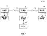
110 X線源(「X線」)
112 フォトン
114 目標物(「目標物」)
116 検出器(「検出器」)
118 取得回路
120 システム制御器
124 I/Oシステム
200 バイア構造
202 バイア構造
204 バイア構造
206 バイア構造
210 基材
212 層
214 金属化層(M1)
216 層
218 金属化層(M2)
220 層
222 金属化層(M3)
224 層
226 ダイオード
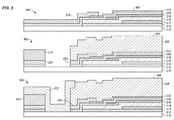
300 工程のステップ
301 最も高い層
302 工程のステップ
303 最も高い層
304 工程のステップ
305 最も高い層
310 ダイオード通過層
312 遮断層
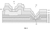
510 金属化層(M4)
512 バイア構造
514 バイア構造
516 金属積層体
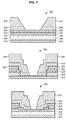
700 ダイオード・バイア
702 ダイオード・バイア
704 ダイオード・バイア
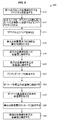
800 方法
810 ブロック
812 ブロック
814 ブロック
816 ブロック
818 ブロック
820 ブロック
822 ブロック
824 ブロック
826 ブロック
828 ブロック
830 ブロック
Claims (10)
- 基材(210)と、
少なくとも1又は複数の金属層、該少なくとも1又は複数の金属層(214、218、222)に配設された誘電体層、及び少なくとも1又は複数の前記金属層にダイオード層を結合するために前記誘電体に形成された1又は複数のバイア(200、202、204、206)を含んでいる第一の面域と、
少なくとも前記基材に前記ダイオード層を接着するために前記誘電体に形成された0以上のバイア(200、202、204、206)を含んでいる第二の面域と、
を備えた装置。 - 前記ダイオード層は、少なくとも1若しくは複数のフォトダイオード(226)、1若しくは複数のPINダイオード、若しくはアモルファス・シリコン、又はこれらの組み合わせを含んでいる、請求項1に記載の装置。
- 前記少なくとも1又は複数の金属層は、第一の金属化層(214)及び第二の金属化層(218)を含んでおり、前記バイアの少なくとも1又は複数は、前記ダイオード層を前記第二の金属化層には接触させずに前記第一の金属化層に接触させることが可能な構造を有する、請求項1に記載の装置。
- 前記少なくとも1又は複数の金属層は、第一の金属化層(214)、第二の金属化層(218)及び第三の金属化層(222)を含んでおり、前記バイアの少なくとも1又は複数は、前記ダイオード層を前記第二の金属化層には接触させずに前記第三の金属化層に接触させることが可能な構造を有する、請求項1に記載の装置。
- 前記少なくとも1又は複数の金属層は、第一の金属化層(214)、第二の金属化層(218)及び第三の金属化層(222)を含んでおり、前記バイアの少なくとも1又は複数は、前記ダイオード層を前記第二の金属化層には接触させずに前記第三の金属化層に接触させることが可能な構造を有し、前記ダイオード層のダイオード(226)は、前記第三の金属化層を介して前記第二の金属化層に接触する、請求項1に記載の装置。
- 前記少なくとも1又は複数の金属層は、第一の金属化層(214)、第二の金属化層(218)及び第三の金属化層(222)を含んでおり、前記バイアの少なくとも1又は複数は、前記ダイオード層を前記第二の金属化層には接触させずに前記第三の金属化層に接触させることが可能な構造を有し、前記第三の金属化層は、モリブデン、モリブデン−タングステン、モリブデン合金、チタン若しくはチタン合金の少なくとも一つ、又はこれらの組み合わせを含んでいる、請求項1に記載の装置。
- 前記少なくとも1又は複数の金属層は、第一の金属化層(214)、第二の金属化層(218)及び第三の金属化層(222)を含んでおり、前記バイアの少なくとも1又は複数は、前記ダイオード層を前記第二の金属化層には接触させずに前記第三の金属化層に接触させることが可能な構造を有し、前記第三の金属化層は、モリブデン、モリブデン−タングステン、モリブデン合金、チタン若しくはチタン合金の少なくとも一つ、又はこれらの組み合わせから成っている、請求項1に記載の装置。
- 前記少なくとも1又は複数の金属層は、第一の金属化層(214)、第二の金属化層(218)及び第三の金属化層(222)を含んでおり、前記バイアの少なくとも1又は複数は、前記ダイオード層を前記第二の金属化層には接触させずに前記第三の金属化層に接触させることが可能な構造を有し、前記第三の金属化層は、モリブデン、モリブデン−タングステン、モリブデン合金、チタン若しくはチタン合金の少なくとも一つ、又はこれらの組み合わせから本質的に成っている、請求項1に記載の装置。
- 前記バイア(200、202、204、206)の少なくとも1又は複数は階段状側壁構造を含んでいる、請求項1に記載の装置。
- 前記バイア(200、202、204、206)の少なくとも1又は複数は、前記ダイオード層が前記バイアの内部に受け入れられたときに前記ダイオード層を前記基材に接触させることが可能な構造を有し、前記バイアは、薄膜トランジスタ・アレイの外部のエッジ・クリア面域、前記薄膜トランジスタ・アレイの不動態化性窒化物層の下方の1若しくは複数の金属化層に近接した面域、前記薄膜トランジスタ・アレイの格子開口の内部の面域、前記薄膜トランジスタ・アレイの電気的非作動性面域、前記薄膜トランジスタ・アレイの1若しくは複数の接点フィンガに隣接する面域、前記薄膜トランジスタ・アレイの1若しくは複数の接点フィンガ上の少なくとも1箇所、又はこれらの組み合わせに配設されている、請求項1に記載の装置。
Applications Claiming Priority (2)
| Application Number | Priority Date | Filing Date | Title |
|---|---|---|---|
| US11/291,602 US7759680B2 (en) | 2005-11-30 | 2005-11-30 | Thin-film transistor and diode array for an imager panel or the like |
| US11/291,602 | 2005-11-30 |
Publications (2)
| Publication Number | Publication Date |
|---|---|
| JP2007158335A true JP2007158335A (ja) | 2007-06-21 |
| JP5155554B2 JP5155554B2 (ja) | 2013-03-06 |
Family
ID=38037993
Family Applications (1)
| Application Number | Title | Priority Date | Filing Date |
|---|---|---|---|
| JP2006323498A Expired - Fee Related JP5155554B2 (ja) | 2005-11-30 | 2006-11-30 | ダイオード層を金属層に結合するためのバイアを備えた装置 |
Country Status (4)
| Country | Link |
|---|---|
| US (1) | US7759680B2 (ja) |
| JP (1) | JP5155554B2 (ja) |
| DE (1) | DE102006056995B4 (ja) |
| FR (1) | FR2894071B1 (ja) |
Cited By (2)
| Publication number | Priority date | Publication date | Assignee | Title |
|---|---|---|---|---|
| JP2009141361A (ja) * | 2007-12-06 | 2009-06-25 | General Electric Co <Ge> | フラット・パネルx線イメージャのコスト軽減型ピクセル設計 |
| KR101769587B1 (ko) | 2011-12-08 | 2017-08-21 | 삼성디스플레이 주식회사 | 엑스레이 검출기 및 엑스레이 검출기 구동 방법 |
Families Citing this family (8)
| Publication number | Priority date | Publication date | Assignee | Title |
|---|---|---|---|---|
| JP5185013B2 (ja) | 2008-01-29 | 2013-04-17 | 富士フイルム株式会社 | 電磁波検出素子 |
| US8736008B2 (en) | 2012-01-04 | 2014-05-27 | General Electric Company | Photodiode array and methods of fabrication |
| US9116249B1 (en) * | 2012-07-26 | 2015-08-25 | Sandia Corporation | Multiple-mode radiation detector |
| WO2016061553A1 (en) * | 2014-10-17 | 2016-04-21 | Silverside Detectors Inc. | Fissile neutron detector |
| US10317541B2 (en) | 2017-04-14 | 2019-06-11 | Silverside Detectors, Inc. | Advanced fissile neutron detection system and method |
| US10302781B2 (en) | 2017-04-15 | 2019-05-28 | Silverside Detectors, Inc. | Advanced thermal neutron detectors and associated methods |
| CN107634079B (zh) * | 2017-09-19 | 2020-05-08 | 中山晟欣信息科技有限公司 | 光电传感器及其制造方法 |
| JP7406887B2 (ja) * | 2019-08-07 | 2023-12-28 | キヤノン株式会社 | 光電変換装置、放射線撮像システム、光電変換システム、移動体 |
Citations (3)
| Publication number | Priority date | Publication date | Assignee | Title |
|---|---|---|---|---|
| JPS5812481A (ja) * | 1981-07-15 | 1983-01-24 | Toshiba Corp | 固体撮像素子 |
| JPH05276442A (ja) * | 1992-03-30 | 1993-10-22 | Hamamatsu Photonics Kk | 残像積分固体撮像デバイス |
| JPH1197660A (ja) * | 1997-09-19 | 1999-04-09 | Semiconductor Energy Lab Co Ltd | イメージセンサおよびそれを用いた装置 |
Family Cites Families (3)
| Publication number | Priority date | Publication date | Assignee | Title |
|---|---|---|---|---|
| US4571626A (en) | 1981-09-17 | 1986-02-18 | Matsushita Electric Industrial Co., Ltd. | Solid state area imaging apparatus |
| US6835974B2 (en) * | 2002-03-14 | 2004-12-28 | Jeng-Jye Shau | Three dimensional integrated circuits using sub-micron thin-film diodes |
| CN100505284C (zh) | 2004-06-18 | 2009-06-24 | 皇家飞利浦电子股份有限公司 | X射线图像检测器 |
-
2005
- 2005-11-30 US US11/291,602 patent/US7759680B2/en active Active
-
2006
- 2006-11-30 DE DE102006056995.4A patent/DE102006056995B4/de not_active Expired - Fee Related
- 2006-11-30 JP JP2006323498A patent/JP5155554B2/ja not_active Expired - Fee Related
- 2006-11-30 FR FR0655222A patent/FR2894071B1/fr not_active Expired - Fee Related
Patent Citations (3)
| Publication number | Priority date | Publication date | Assignee | Title |
|---|---|---|---|---|
| JPS5812481A (ja) * | 1981-07-15 | 1983-01-24 | Toshiba Corp | 固体撮像素子 |
| JPH05276442A (ja) * | 1992-03-30 | 1993-10-22 | Hamamatsu Photonics Kk | 残像積分固体撮像デバイス |
| JPH1197660A (ja) * | 1997-09-19 | 1999-04-09 | Semiconductor Energy Lab Co Ltd | イメージセンサおよびそれを用いた装置 |
Cited By (2)
| Publication number | Priority date | Publication date | Assignee | Title |
|---|---|---|---|---|
| JP2009141361A (ja) * | 2007-12-06 | 2009-06-25 | General Electric Co <Ge> | フラット・パネルx線イメージャのコスト軽減型ピクセル設計 |
| KR101769587B1 (ko) | 2011-12-08 | 2017-08-21 | 삼성디스플레이 주식회사 | 엑스레이 검출기 및 엑스레이 검출기 구동 방법 |
Also Published As
| Publication number | Publication date |
|---|---|
| DE102006056995A1 (de) | 2007-05-31 |
| FR2894071A1 (fr) | 2007-06-01 |
| US20070122948A1 (en) | 2007-05-31 |
| FR2894071B1 (fr) | 2016-01-01 |
| JP5155554B2 (ja) | 2013-03-06 |
| DE102006056995B4 (de) | 2018-03-22 |
| US7759680B2 (en) | 2010-07-20 |
Similar Documents
| Publication | Publication Date | Title |
|---|---|---|
| US7468531B2 (en) | Imaging apparatus and radiation imaging apparatus | |
| JP4147186B2 (ja) | 感光及び/又は感x線センサからなるセンサ配置 | |
| CN102810547B (zh) | 检测器件制造方法、检测器件和检测系统 | |
| US20080237474A1 (en) | Semiconductor photodiode and method for manufacturing same, radiation detection device, and radiation imaging apparatus | |
| CN102810548B (zh) | 检测器件制造方法、检测器件和检测系统 | |
| JP2009252835A (ja) | 電磁波検出素子 | |
| US20130299711A1 (en) | Detection device, detection system, and method of manufacturing detection device | |
| WO2007007881A1 (en) | Conversion apparatus, radiation detecting apparatus, and radiation detecting system | |
| JP2006504258A (ja) | 回路基板およびその製造方法 | |
| TWI734051B (zh) | 陣列基板、包含該陣列基板的數位x光檢測器、以及製造該陣列基板的方法 | |
| JP5739359B2 (ja) | 撮像装置およびその製造方法ならびに撮像表示システム | |
| CN102096089A (zh) | 检测x射线的光电二极管及其制造方法 | |
| CN112928179B (zh) | 薄膜晶体管阵列基板和包括其的数字x射线检测器装置 | |
| JP5155554B2 (ja) | ダイオード層を金属層に結合するためのバイアを備えた装置 | |
| JP2013161810A (ja) | 撮像装置およびその製造方法ならびに撮像表示システム | |
| JP2014116429A (ja) | 撮像装置及び撮像表示システム | |
| JP2014236162A (ja) | 検出装置、その製造方法及び放射線検出システム | |
| CN103579271A (zh) | 检测装置、检测系统和检测装置的制造方法 | |
| TWI659223B (zh) | X射線感測裝置及其製造方法 | |
| KR101941426B1 (ko) | 이미지센서 및 그 제조방법 | |
| JP2010003766A (ja) | 電磁波検出素子 | |
| JP2014225524A (ja) | 検出装置の製造方法、その検出装置、及び、検出システム | |
| JP4054612B2 (ja) | 放射線撮像装置 | |
| CN112992943B (zh) | 薄膜晶体管阵列基板及其制造方法和数字x射线探测器装置 | |
| US20230086700A1 (en) | Photodetection device |
Legal Events
| Date | Code | Title | Description |
|---|---|---|---|
| A621 | Written request for application examination |
Free format text: JAPANESE INTERMEDIATE CODE: A621 Effective date: 20091126 |
|
| RD04 | Notification of resignation of power of attorney |
Free format text: JAPANESE INTERMEDIATE CODE: A7424 Effective date: 20091126 |
|
| A521 | Request for written amendment filed |
Free format text: JAPANESE INTERMEDIATE CODE: A523 Effective date: 20101119 |
|
| A131 | Notification of reasons for refusal |
Free format text: JAPANESE INTERMEDIATE CODE: A131 Effective date: 20120327 |
|
| A977 | Report on retrieval |
Free format text: JAPANESE INTERMEDIATE CODE: A971007 Effective date: 20120329 |
|
| A521 | Request for written amendment filed |
Free format text: JAPANESE INTERMEDIATE CODE: A523 Effective date: 20120620 |
|
| A131 | Notification of reasons for refusal |
Free format text: JAPANESE INTERMEDIATE CODE: A131 Effective date: 20120724 |
|
| A521 | Request for written amendment filed |
Free format text: JAPANESE INTERMEDIATE CODE: A523 Effective date: 20121017 |
|
| TRDD | Decision of grant or rejection written | ||
| A01 | Written decision to grant a patent or to grant a registration (utility model) |
Free format text: JAPANESE INTERMEDIATE CODE: A01 Effective date: 20121113 |
|
| A61 | First payment of annual fees (during grant procedure) |
Free format text: JAPANESE INTERMEDIATE CODE: A61 Effective date: 20121207 |
|
| FPAY | Renewal fee payment (event date is renewal date of database) |
Free format text: PAYMENT UNTIL: 20151214 Year of fee payment: 3 |
|
| R150 | Certificate of patent or registration of utility model |
Ref document number: 5155554 Country of ref document: JP Free format text: JAPANESE INTERMEDIATE CODE: R150 Free format text: JAPANESE INTERMEDIATE CODE: R150 |
|
| R250 | Receipt of annual fees |
Free format text: JAPANESE INTERMEDIATE CODE: R250 |
|
| R250 | Receipt of annual fees |
Free format text: JAPANESE INTERMEDIATE CODE: R250 |
|
| R250 | Receipt of annual fees |
Free format text: JAPANESE INTERMEDIATE CODE: R250 |
|
| R250 | Receipt of annual fees |
Free format text: JAPANESE INTERMEDIATE CODE: R250 |
|
| R250 | Receipt of annual fees |
Free format text: JAPANESE INTERMEDIATE CODE: R250 |
|
| LAPS | Cancellation because of no payment of annual fees |