JP2007192578A - Semiconductor inspection device - Google Patents
Semiconductor inspection device Download PDFInfo
- Publication number
- JP2007192578A JP2007192578A JP2006008875A JP2006008875A JP2007192578A JP 2007192578 A JP2007192578 A JP 2007192578A JP 2006008875 A JP2006008875 A JP 2006008875A JP 2006008875 A JP2006008875 A JP 2006008875A JP 2007192578 A JP2007192578 A JP 2007192578A
- Authority
- JP
- Japan
- Prior art keywords
- handler
- handlers
- test head
- connection position
- semiconductor inspection
- Prior art date
- Legal status (The legal status is an assumption and is not a legal conclusion. Google has not performed a legal analysis and makes no representation as to the accuracy of the status listed.)
- Granted
Links
- 239000004065 semiconductor Substances 0.000 title claims abstract description 43
- 238000007689 inspection Methods 0.000 title claims abstract description 25
- 238000012360 testing method Methods 0.000 claims abstract description 45
- 238000004891 communication Methods 0.000 claims description 2
- 239000013256 coordination polymer Substances 0.000 abstract description 18
- 238000004519 manufacturing process Methods 0.000 abstract description 5
- 238000000034 method Methods 0.000 description 4
- 230000008878 coupling Effects 0.000 description 3
- 238000010168 coupling process Methods 0.000 description 3
- 238000005859 coupling reaction Methods 0.000 description 3
- 238000010586 diagram Methods 0.000 description 3
- 238000007796 conventional method Methods 0.000 description 2
- 238000004904 shortening Methods 0.000 description 2
- 238000012546 transfer Methods 0.000 description 2
- 238000003795 desorption Methods 0.000 description 1
- 238000009434 installation Methods 0.000 description 1
- 239000000463 material Substances 0.000 description 1
Images


Landscapes
- Testing Of Individual Semiconductor Devices (AREA)
Abstract
Description
本発明は、半導体検査装置に関する。 The present invention relates to a semiconductor inspection apparatus.
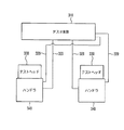
従来から、組立が完了した半導体装置を検査して選別する際に、半導体装置が収容されたハンドラをテストヘッドに連結して、半導体装置の電気的特性が試験されるものが知られている(例えば、特許文献1参照)。このような半導体検査装置においては、図6に示すように、ハンドラ340とテストヘッド330が連結された状態で半導体装置の試験が可能な状態となり、ハンドラ340とテスタ本体310を接続するケーブル320によりテスタ本体310に電気的信号が送信される。図6は従来の半導体検査装置の概略構成説明図である。ところで、半導体装置においては多品種少量生産が進んでおり、選別工程において、異なったパッケージの半導体装置を検査するために、テストヘッド330に連結されるハンドラ340の入れ替えを頻繁に実施している。
2. Description of the Related Art Conventionally, when a semiconductor device that has been assembled is inspected and selected, a handler in which the semiconductor device is accommodated is connected to a test head to test the electrical characteristics of the semiconductor device ( For example, see Patent Document 1). In such a semiconductor inspection apparatus, as shown in FIG. 6, the semiconductor device can be tested in a state where the
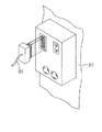
ハンドラ340の入れ替えに際しては、テストヘッド330に連結されているハンドラ340の電源をOFFとし、図7に示すようにハンドラ340のケーブル320をテスタ本体310から取り外す。図7は、従来のハンドラにおけるケーブル脱着の動作を示す説明図である。次いで、図8に示すように、電動リフタ400でハンドラ340を他の場所へ搬送し、次に連結するハンドラ340を電動リフタ400でテストヘッド330との連結位置まで搬送する。図8は、従来のハンドラを電動リフタにより搬送する状態を示す説明図である。そして、ハンドラ340をテストヘッド330に対して位置決め調整して連結し、図7に示すようにテスタ本体310にケーブル320を接続する。
しかしながら、この半導体の検査方法では、作業者が電動リフタ400を利用してハンドラ340を移動させているため、ハンドラ340の入れ替えに多大な時間を要し、半導体の選別工程の工数が嵩んでしまう。また、電動リフタ400による作業は、安全面で好ましいものとはいえない。
However, in this semiconductor inspection method, since the operator moves the
本発明によれば、テスタ本体とケーブルにより接続されるとともに、テストヘッドと連結可能な複数のハンドラと、前記各ハンドラを、前記テストヘッドと連結される連結位置と、該連結位置から離隔した待機位置と、の間で移動自在とするハンドラ移動部と、を備え、前記連結位置にて前記複数のハンドラのうちの一つが前記テストヘッドと選択的に連結されることを特徴とする半導体検査装置が提供される。 According to the present invention, a plurality of handlers that are connected to the tester main body by a cable and can be connected to a test head, a connection position at which each handler is connected to the test head, and a standby that is separated from the connection position And a handler moving unit that is movable between the position and one of the plurality of handlers is selectively coupled to the test head at the coupling position. Is provided.
この半導体検査装置では、ハンドラ移動部により各ハンドラが案内されるので、各ハンドラをリフタ等の搬送装置により移動させる従来の方式に比べて安全性が向上するのは勿論のこと、作業者の負担を軽減するとともに、テストヘッドに連結されるハンドラを入れ替える時間を短縮することができる。 In this semiconductor inspection apparatus, since each handler is guided by the handler moving unit, the safety is improved as compared with the conventional method in which each handler is moved by a transfer device such as a lifter. And the time for replacing the handler connected to the test head can be shortened.
本発明によれば、ハンドラの入れ替えに要する工数を低減して、半導体装置の製造コストを低減することができる。また、ハンドラを入れ替える時間を短縮することで、テスタ本体の稼働率を向上させることができ、これによっても製造コストの低減を図ることができる。 According to the present invention, it is possible to reduce the man-hours required for replacing the handler and reduce the manufacturing cost of the semiconductor device. Further, by shortening the time for replacing the handler, the operating rate of the tester main body can be improved, and the manufacturing cost can also be reduced.
図面を参照しつつ、本発明による検査装置及び検査方法の好適な実施形態について詳細に説明する。尚、図面の説明においては、同一要素には同一符号を付し、重複する説明を省略する。 A preferred embodiment of an inspection apparatus and an inspection method according to the present invention will be described in detail with reference to the drawings. In the description of the drawings, the same elements are denoted by the same reference numerals, and redundant description is omitted.
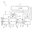
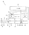
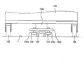
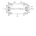
図1から図5は本発明の一実施形態を示すものであり、図1は第1ハンドラがテストヘッドに接続された半導体検査装置の概略構成説明図、図2は第2ハンドラがテストヘッドに接続された半導体検査装置の概略構成説明図、図3は第1ハンドラの下部正面図、図4は第1ハンドラの概略底面図である。 FIGS. 1 to 5 show an embodiment of the present invention. FIG. 1 is a schematic diagram for explaining the configuration of a semiconductor inspection apparatus in which a first handler is connected to a test head. FIG. FIG. 3 is a lower front view of the first handler, and FIG. 4 is a schematic bottom view of the first handler.
図1に示すように、この半導体検査装置100は、テスタ本体110とケーブル120により接続されるとともに第1テストヘッド130と連結可能な第1ハンドラ140及び第2ハンドラ150を備えている。また、半導体検査装置100は、各ハンドラ140,150を第1テストヘッド130と連結される連結位置CPと、連結位置CPから離隔した待機位置WPと、の間で移動自在とするハンドラ移動部160を備え、連結位置CPにて第1ハンドラ140と第2ハンドラ150のうちの一つが第1テストヘッド130と選択的に連結される(図1及び図2参照)。
As shown in FIG. 1, the
また、半導体検査装置100は、テスタ本体110とケーブル170により接続されるとともに第2テストヘッド180と連結される第3ハンドラ190を備えている。第3ハンドラ190は、第2テストヘッド180と連結された状態で位置決め固定されている。
In addition, the
各ハンドラ140,150,190には組立が完了した半導体装置が収容されている。そして、各ハンドラ140,150,190が各テストヘッド130,180と連結された状態で、テストヘッド130,180へ半導体装置が供給され、テスタ本体110により半導体装置の電気的な良否判定が行われる。この判定結果に基づいて各ハンドラ140,150,190が動作するようになっている。
Each
図3に示すように、ハンドラ移動部160は、床面Fに設けられ各ハンドラ140,150を案内するレール162と各ハンドラ140,150に設けられレール162と当接する補助輪164と、各ハンドラ140,150に設けられ床面Fに接地するキャスタ166と、を有する。図3では、第1ハンドラ140について例示しているが、第2ハンドラ150についても同様の構成になっている。
As shown in FIG. 3, the
図1及び図2に示すように、レール162は第1ハンドラ140の待機位置WPから連結位置CPを経由して第2ハンドラ150の待機位置WPまで延びている。本実施形態においては、レール162はほぼ一直線状に形成され、レール162の一端側で第1ハンドラ140が往復し、他端側で第2ハンドラ150が往復する。図3に示すように、レール162は、断面が下面を開放した凹状を呈し、床面Fとともに閉断面をなしている。
As shown in FIGS. 1 and 2, the
図3に示すように、補助輪164は、レール162の側壁上を転動し、レール162を挟み込むよう各ハンドラ140,150の下部に一対に設けられる。詳しくは、各補助輪164は上下に延びる回転軸164aに軸支され、各回転軸164aは支持材164bに固定されている。支持材164bは、ハンドラ140,150の床下部材164cの下端に固定されている。図4に示すように、キャスタ166は、各ハンドラ140,150の下面の四隅に取り付けられ、床面Fに対して各ハンドラ140,150を移動自在としている。
As shown in FIG. 3, the
図5は、位置決めされた第1ハンドラの外観斜視図であり、(a)は連結位置に位置決めされた状態を示し、(b)は待機位置に位置決めされた状態を示す。
図5に示すように、半導体検査装置100は、各ハンドラ140,150を連結位置CP及び待機位置WPで位置決めする位置決め部200を備えている。位置決め部200は、各ハンドラ140,150の側部に設けられたピン部材202と、連結位置CP及び待機位置WPの床面F側に設けられピン部材202を受容する穴部204と、を有している。
FIGS. 5A and 5B are external perspective views of the positioned first handler. FIG. 5A shows a state where the first handler is positioned at the connection position, and FIG. 5B shows a state where the first handler is positioned at the standby position.
As shown in FIG. 5, the
図5に示すように、ピン部材202は上下に移動自在であり、上端に操作レバー206が形成されている。作業者は、操作レバー206を用いてピン部材202を穴部204に対して挿抜することにより、各ハンドラ140,150の位置決めを行うことができる。レール162の一端側に配される第1ハンドラ140については、ピン部材202が一端側の側部に設けられる。また、レール162の他端側に配される第2ハンドラ150については、ピン部材202が他端側の側部に設けられる。
As shown in FIG. 5, the
図5(a)に示すように、連結位置CPにおいては穴部204はレール162の上面に形成される。なお、連結位置CPにおける穴部204は、第1ハンドラ140と第2ハンドラ150とで別個に形成される。これは、図1及び図2に示すように、第1ハンドラ140と第2ハンドラ150で連結位置CPにおけるピン部材202の位置がレール162の長手方向について逆さとなるからである。第1ハンドラ140用の穴部204はレール162の一端側に形成され、第2ハンドラ150用の穴部204はレール162の他端側に形成される。
As shown in FIG. 5A, the
また、図5(b)に示すように、待機位置WPにおいては穴部204は端部ブロック208の上面に形成される。端部ブロック208は、レール162の両端位置にてレール162と略垂直に延びるよう床面Fに設置されている。すなわち、各端部ブロック208は各ハンドラ140,150の移動を規制するストッパとして機能する。
Further, as shown in FIG. 5B, the
また、図1及び図2に示すように、半導体検査装置100は、ケーブル120においてテスタ本体110と各ハンドラ140,150との間に介在し、テスタ本体110との通信に使用するケーブル120を切替自在にしている切替部210を備えている。切替部210は第1テストヘッド130に設置され、図示しない切替スイッチが設けられている。作業者は、切替スイッチを操作することにより、第1ハンドラ140のケーブル120と、第2ハンドラ150のケーブル120のいずれを使用するかを選択することができ、連結位置にあるハンドラとテスタ本体110とを通信可能にすることができる。各ケーブル120における各ハンドラ140,150と切替部210の間の部分は弛張自在となっており、各ハンドラ140,150の可動範囲で各ケーブル120により各ハンドラ140,150が拘束されることはない。尚、第3ハンドラ190のケーブル170は、テスタ本体110に直接接続されている。
Further, as shown in FIGS. 1 and 2, the
以上のように構成された半導体検査装置100では、テスタ本体110により、第1テストヘッド130と第2テストヘッド180で同時に半導体装置の試験が行われる。
第1テストヘッド130における各ハンドラ140,150の入れ替えに際して、作業者は、ピン部材202を穴部204から抜脱して各ハンドラ140,150をレール162に沿って移動可能な状態とする。この後、各ハンドラ140,150を連結位置CP及び待機位置WPに移動させて、ピン部材202を穴部204に挿入して位置決めを行う。そして、切替部210にてケーブル120の切替操作を行い、新たに連結されたハンドラ140,150のケーブル120を使用可能な状態とする。
In the
When replacing the
このとき、ハンドラ移動部160により各ハンドラ140,150が案内されるので、各ハンドラ140,150をリフタ等の搬送装置により移動させる従来の方式に比べて、作業者の負担を軽減するとともに、第1テストヘッド130に連結されるハンドラ140,150を入れ替える時間を短縮することができる。これにより、ハンドラ140,150の入れ替えに要する工数を低減して、半導体装置の製造コストを低減することができる。さらに、ハンドラ140,150を入れ替える時間を短縮することで、テスタ本体110の稼働率を向上させることができ、これによっても製造コストの低減を図ることができる。
At this time, since the
また、切替部210にてケーブル120の切替を行うようにしたので、ハンドラ140,150の入れ替え時に従来のようなケーブルの脱着作業が発生することはなく、これによっても、作業者の負担を軽減するとともに、第1テストヘッド130に連結されるハンドラ140,150を入れ替える時間を短縮することができる。
Further, since the
また、各ハンドラ140,150が所定の連結位置CPにて第1テストヘッド130と連結されるので、第1テストヘッド130と連結されるハンドラ140,150を入れ替えて再連結した際に、同様の連結状態を再現することができる。これにより、テスタ本体110を安定的に稼働させて、半導体装置の検査を的確に行うことができ、半導体装置の品質を担保することができる。
Further, since each
これに対し、従来の半導体検査装置では、ハンドラの連結位置への移動を目視にて行っているので、テストヘッドと連結する都度にハンドラの位置が異なることが多く、同様の連結状態を再現し難い。これにより、テスタ本体を安定的に稼働させることができず、半導体装置の品質が低下するおそれがある。 On the other hand, in the conventional semiconductor inspection apparatus, since the handler is visually moved to the connection position, the position of the handler is often different every time it is connected to the test head, and the same connection state is reproduced. hard. As a result, the tester body cannot be stably operated, and the quality of the semiconductor device may be deteriorated.
また、各ハンドラ140,150が連結位置CPで位置決めされるので、各ハンドラ140,150の第1テストヘッド130への連結状態を的確に再現することができる。また、各ハンドラ140,150が待機位置WPにて位置決めされるので、使用していない各ハンドラ140,150に外力が作用した場合に各ハンドラ140,150が移動してしまうようなことはない。
Further, since the
尚、前記実施形態においては、第3ハンドラ190及び第2テストヘッド180を備え、同時に2種類の半導体装置を検査するものを示したが、これらを備えず1種類の半導体装置を検査するものであってもよい。この逆に、さらにハンドラ及びテストヘッドを備えて、同時に3種類以上の半導体装置を検査するものであってもよい。
In the above embodiment, the
また、前記実施形態においては、ハンドラ移動部160がレール162を有するものを示したが、例えば、キャスタ166が受容され待機位置WPから連結位置CPまで延びる床面Fに溝を形成して各ハンドラ140,150を移動自在としてもよく、要は、連結位置CPと待機位置WPの間でハンドラ140,150が移動自在であればよい。
In the above embodiment, the
また、前記実施形態においては、第1ハンドラ140及び第2ハンドラ150のケーブル120が切替部210に接続されるものを示したが、各ケーブル120がテスタ本体110に直接接続されているものであってもよい。また、切替部210は、前記実施形態のように手動でケーブル120を切り替えるものでなく、外部からの信号等により自動的にケーブル120を切り替えるものであってもよい。さらに、切替部210の設置場所は任意であるし、その他、具体的な細部構造等についても適宜に変更可能であることは勿論である。
In the above embodiment, the
100 半導体検査装置
110 テスタ本体
120 ケーブル
130 第1テストヘッド
140 第1ハンドラ
150 第2ハンドラ
160 ハンドラ移動部
162 レール
164 補助輪
164a 回転軸
164b 支持材
164c 床下部材
166 キャスタ
170 ケーブル
180 第2テストヘッド
190 第3ハンドラ
200 位置決め部
202 ピン部材
204 穴部
206 操作レバー
208 端部ブロック
210 切替部
310 テスタ本体
320 ケーブル
330 テストヘッド
340 ハンドラ
400 電動リフタ
CP 連結位置
F 床面
WP 待機位置
DESCRIPTION OF
Claims (4)
前記各ハンドラを、前記テストヘッドと連結される連結位置と、該連結位置から離隔した待機位置と、の間で移動自在とするハンドラ移動部と、を備え、
前記連結位置にて前記複数のハンドラのうちの一つが前記テストヘッドと選択的に連結されることを特徴とする半導体検査装置。 A plurality of handlers that can be connected to the test head and connected to the test head,
A handler moving unit that allows each of the handlers to move between a connection position connected to the test head and a standby position spaced apart from the connection position;
A semiconductor inspection apparatus, wherein one of the plurality of handlers is selectively connected to the test head at the connection position.
4. The semiconductor inspection apparatus according to claim 1, wherein the handler moving unit includes a rail that extends from the connection position to the standby position and guides each of the handlers.
Priority Applications (1)
| Application Number | Priority Date | Filing Date | Title |
|---|---|---|---|
| JP2006008875A JP4695987B2 (en) | 2006-01-17 | 2006-01-17 | Semiconductor inspection equipment |
Applications Claiming Priority (1)
| Application Number | Priority Date | Filing Date | Title |
|---|---|---|---|
| JP2006008875A JP4695987B2 (en) | 2006-01-17 | 2006-01-17 | Semiconductor inspection equipment |
Publications (2)
| Publication Number | Publication Date |
|---|---|
| JP2007192578A true JP2007192578A (en) | 2007-08-02 |
| JP4695987B2 JP4695987B2 (en) | 2011-06-08 |
Family
ID=38448407
Family Applications (1)
| Application Number | Title | Priority Date | Filing Date |
|---|---|---|---|
| JP2006008875A Expired - Fee Related JP4695987B2 (en) | 2006-01-17 | 2006-01-17 | Semiconductor inspection equipment |
Country Status (1)
| Country | Link |
|---|---|
| JP (1) | JP4695987B2 (en) |
Citations (5)
| Publication number | Priority date | Publication date | Assignee | Title |
|---|---|---|---|---|
| JPS60114978U (en) * | 1984-01-10 | 1985-08-03 | 日本電気株式会社 | IC test equipment |
| JPH0357940U (en) * | 1989-10-06 | 1991-06-05 | ||
| JPH0513535A (en) * | 1991-07-05 | 1993-01-22 | Mitsubishi Electric Corp | Test head attachment / detachment device |
| JPH08211123A (en) * | 1994-11-24 | 1996-08-20 | Advantest Corp | Semiconductor test equipment equipped with test head connection device |
| JP2003098224A (en) * | 2001-09-25 | 2003-04-03 | Santo Technology Kk | Semiconductor test equipment |
-
2006
- 2006-01-17 JP JP2006008875A patent/JP4695987B2/en not_active Expired - Fee Related
Patent Citations (5)
| Publication number | Priority date | Publication date | Assignee | Title |
|---|---|---|---|---|
| JPS60114978U (en) * | 1984-01-10 | 1985-08-03 | 日本電気株式会社 | IC test equipment |
| JPH0357940U (en) * | 1989-10-06 | 1991-06-05 | ||
| JPH0513535A (en) * | 1991-07-05 | 1993-01-22 | Mitsubishi Electric Corp | Test head attachment / detachment device |
| JPH08211123A (en) * | 1994-11-24 | 1996-08-20 | Advantest Corp | Semiconductor test equipment equipped with test head connection device |
| JP2003098224A (en) * | 2001-09-25 | 2003-04-03 | Santo Technology Kk | Semiconductor test equipment |
Also Published As
| Publication number | Publication date |
|---|---|
| JP4695987B2 (en) | 2011-06-08 |
Similar Documents
| Publication | Publication Date | Title |
|---|---|---|
| KR101168903B1 (en) | Test head and semiconductor wafer testing apparatus provided with the same | |
| KR101606569B1 (en) | Vehicle cable inspection apparatus | |
| EP1495339B1 (en) | Semiconductor test system with easily changed interface unit | |
| WO2007130763A1 (en) | Automated programming system employing smart interfaces | |
| JP2009505417A (en) | Test handler | |
| JP2013118770A (en) | Electric vehicle control device | |
| JP4695987B2 (en) | Semiconductor inspection equipment | |
| JP2006322918A (en) | Interface and semiconductor test apparatus using the same | |
| JP2010067679A (en) | Apparatus for mounting electronic component and carriage for replacing parts feeder | |
| CN103728505B (en) | Check device | |
| JPH0254877A (en) | Automatic connecting device | |
| EP1604799A1 (en) | Extracting device for molded articles | |
| JP2001201528A (en) | Continuity test equipment for wiring boards, etc. | |
| JP2006181680A (en) | Work positioning and conveying apparatus, work positioning method and work positioning and conveying cart | |
| CN109906004B (en) | Automatic wiring robot | |
| JP2006308450A (en) | Exchange device for work table receiving display substrate and inspection device for display substrate | |
| KR20070028023A (en) | Test jig unit | |
| KR20090063721A (en) | Automotive Fuse Puller | |
| JP4172546B2 (en) | Connection system for vehicle running test | |
| JP2005523457A (en) | Single axis manipulator with controlled compliance | |
| JP4960147B2 (en) | Electronic component mounting apparatus main body and electronic component mounting apparatus | |
| KR102928673B1 (en) | Electrical switchgear | |
| JP4685336B2 (en) | TFT array inspection equipment | |
| KR20070024796A (en) | Probe card cleaning device | |
| CN204631561U (en) | Embedded machine tool control cabinet |
Legal Events
| Date | Code | Title | Description |
|---|---|---|---|
| A621 | Written request for application examination |
Effective date: 20081113 Free format text: JAPANESE INTERMEDIATE CODE: A621 |
|
| A977 | Report on retrieval |
Effective date: 20100927 Free format text: JAPANESE INTERMEDIATE CODE: A971007 |
|
| A131 | Notification of reasons for refusal |
Effective date: 20101012 Free format text: JAPANESE INTERMEDIATE CODE: A131 |
|
| A521 | Written amendment |
Free format text: JAPANESE INTERMEDIATE CODE: A523 Effective date: 20101202 |
|
| A131 | Notification of reasons for refusal |
Free format text: JAPANESE INTERMEDIATE CODE: A131 Effective date: 20101221 |
|
| A521 | Written amendment |
Free format text: JAPANESE INTERMEDIATE CODE: A523 Effective date: 20110201 |
|
| TRDD | Decision of grant or rejection written | ||
| A01 | Written decision to grant a patent or to grant a registration (utility model) |
Free format text: JAPANESE INTERMEDIATE CODE: A01 Effective date: 20110222 |
|
| A01 | Written decision to grant a patent or to grant a registration (utility model) |
Free format text: JAPANESE INTERMEDIATE CODE: A01 |
|
| A61 | First payment of annual fees (during grant procedure) |
Effective date: 20110228 Free format text: JAPANESE INTERMEDIATE CODE: A61 |
|
| FPAY | Renewal fee payment (prs date is renewal date of database) |
Free format text: PAYMENT UNTIL: 20140304 Year of fee payment: 3 |
|
| R150 | Certificate of patent (=grant) or registration of utility model |
Free format text: JAPANESE INTERMEDIATE CODE: R150 |
|
| LAPS | Cancellation because of no payment of annual fees |