JP2007192806A - Target substance detection element substrate, target substance detection element, target substance detection apparatus and method using the same, and kit for the same - Google Patents
Target substance detection element substrate, target substance detection element, target substance detection apparatus and method using the same, and kit for the same Download PDFInfo
- Publication number
- JP2007192806A JP2007192806A JP2006320305A JP2006320305A JP2007192806A JP 2007192806 A JP2007192806 A JP 2007192806A JP 2006320305 A JP2006320305 A JP 2006320305A JP 2006320305 A JP2006320305 A JP 2006320305A JP 2007192806 A JP2007192806 A JP 2007192806A
- Authority
- JP
- Japan
- Prior art keywords
- target substance
- detection element
- metal pattern
- pattern layer
- sample solution
- Prior art date
- Legal status (The legal status is an assumption and is not a legal conclusion. Google has not performed a legal analysis and makes no representation as to the accuracy of the status listed.)
- Pending
Links
Images









Classifications
-
- G—PHYSICS
- G01—MEASURING; TESTING
- G01N—INVESTIGATING OR ANALYSING MATERIALS BY DETERMINING THEIR CHEMICAL OR PHYSICAL PROPERTIES
- G01N21/00—Investigating or analysing materials by the use of optical means, i.e. using sub-millimetre waves, infrared, visible or ultraviolet light
- G01N21/17—Systems in which incident light is modified in accordance with the properties of the material investigated
- G01N21/55—Specular reflectivity
- G01N21/552—Attenuated total reflection
- G01N21/553—Attenuated total reflection and using surface plasmons
Landscapes
- Physics & Mathematics (AREA)
- Health & Medical Sciences (AREA)
- Life Sciences & Earth Sciences (AREA)
- Chemical & Material Sciences (AREA)
- Analytical Chemistry (AREA)
- Biochemistry (AREA)
- General Health & Medical Sciences (AREA)
- General Physics & Mathematics (AREA)
- Immunology (AREA)
- Pathology (AREA)
- Automatic Analysis And Handling Materials Therefor (AREA)
- Investigating Or Analysing Materials By Optical Means (AREA)
Abstract
【課題】標的物質を捕捉する化学センサの更なる性能向上を図ること。
【解決手段】検体中の標的物質を、プラズモン共鳴法を利用して検出するために用いられる素子であって、水と同等の屈折率を有する下地層上に金属パターン層を設け、金属パターン層に標的物質捕捉体を固定して標的物質検出素子を作製する。
【選択図】図1To further improve the performance of a chemical sensor for capturing a target substance.
An element used for detecting a target substance in a specimen using a plasmon resonance method, wherein a metal pattern layer is provided on an underlayer having a refractive index equivalent to that of water, and the metal pattern layer A target substance detection element is prepared by fixing a target substance capturing body to the substrate.
[Selection] Figure 1
Description
本発明は、試料溶液中における標的物質の有無を検出するために有用な標的物質検出用の素子及びその作製のための基板、並びに、標的物質検出装置、検出方法及び検出用キットに関する。 The present invention relates to an element for detecting a target substance useful for detecting the presence or absence of a target substance in a sample solution, a substrate for producing the element, a target substance detection apparatus, a detection method, and a detection kit.
センサの一形態としてバイオセンサがある。バイオセンサは、生体や生体分子の持つ優れた生体分子認識能を利用した計測デバイスであり、近年、医療分野のみならず、環境や食料品等への幅広い応用が期待されている。一般的に、バイオセンサは、測定対象とする物質(以下、標的物質)を認識、捕捉する捕捉体と、その時発生する物理的、化学的な変化を検知し、電気信号、光信号等の検出可能な信号へ変換する検出素子と、から構成される。生体内には、互いに親和性のある物質の組み合わせとして、例えば酵素−基質、抗原−抗体、DNA−DNA等がある。バイオセンサではこれらの組み合わせの一方を基材に固定化もしくは担持し、捕捉体成分として用いることによって、もう一方の物質を選択的に計測できるという原理を利用している。また、検出素子としては、酸素電極、過酸化水素電極、イオン電極、ISFET、サーミスタなど様々な形式のものが提案されており、最近ではナノグラム程度の質量変化が検知できる水晶振動子やSAW素子、プラズモン共鳴素子などが使われる場合もある。 One form of sensor is a biosensor. A biosensor is a measuring device that uses the excellent biomolecule recognition ability of a living body or a biomolecule, and has recently been expected to be widely applied not only to the medical field but also to the environment, food products, and the like. In general, a biosensor detects a capture object that recognizes and captures a substance to be measured (hereinafter referred to as a target substance) and physical and chemical changes that occur at that time, and detects electrical signals, optical signals, and the like. And a detection element that converts the signal into a possible signal. In the living body, there are, for example, enzyme-substrate, antigen-antibody, DNA-DNA and the like as combinations of substances having affinity for each other. Biosensors use the principle that one of these combinations can be immobilized or supported on a substrate and used as a trap component to selectively measure the other substance. In addition, various types of detection elements such as an oxygen electrode, a hydrogen peroxide electrode, an ion electrode, an ISFET, and a thermistor have been proposed. Recently, a crystal resonator or a SAW element capable of detecting a mass change of about nanograms, A plasmon resonance element may be used.
各種のセンサの中で、プラズモン共鳴を利用した検出系を利用するセンサは、以下の特長を有している。
(1)蛍光色素などの標識分子が必要でないためアッセイの構成が簡単である。
(2)金属微粒子表面への吸着反応の過程を直接リアルタイム・モニタリングできる。
Among various sensors, a sensor using a detection system using plasmon resonance has the following features.
(1) Since a labeling molecule such as a fluorescent dye is not required, the assay configuration is simple.
(2) The process of the adsorption reaction on the surface of the metal fine particles can be directly monitored in real time.
そこで、この測定法は各種のアッセイへの適用が期待されている。 Therefore, this measurement method is expected to be applied to various assays.
この測定法では、金や銀等の金属微粒子を基板表面に固定化し、この金属微粒子に光を入射した際に、そこに誘起される局在プラズモン共鳴により特徴的な共鳴スペクトルが現れることを利用して金属微粒子近傍の物質の検出が行なわれる。その共鳴波長は金属微粒子近傍の媒質の誘電率に依存することが知られている。その誘電率が大きくなるに従い、共鳴ピークの吸光度は大きくなり、長波長側へシフトするようになる。例えば、特許第3452837号明細書には、直径約20nmの金コロイドを用いた系が提案されている。これは、基板に固定した金属微粒子の直径程度の距離までにある媒質の屈折率を検出するようにしたものであり、その結果、金属微粒子表面への物質の吸着や堆積を検出することができる。 This measurement method utilizes the fact that metal particles such as gold and silver are immobilized on the substrate surface, and when a light is incident on the metal particles, a characteristic resonance spectrum appears due to localized plasmon resonance induced there. Thus, the substance in the vicinity of the metal fine particles is detected. It is known that the resonance wavelength depends on the dielectric constant of the medium near the metal fine particles. As the dielectric constant increases, the absorbance at the resonance peak increases and shifts to the longer wavelength side. For example, Japanese Patent No. 342837 proposes a system using a gold colloid having a diameter of about 20 nm. This is to detect the refractive index of the medium up to the distance of the diameter of the metal fine particles fixed to the substrate, and as a result, it is possible to detect the adsorption and deposition of substances on the surface of the metal fine particles. .
一方、Felicia Tamら(J.Phys.Chem.B.、2004年、108巻、45号、p.17290−17294)にあるように、誘電体の核に金薄膜をコートしたコアシェル型の微粒子を作製し、検出能力の向上を図っている素子構成例もある。 On the other hand, as described in Felicia Tam et al. (J. Phys. Chem. B., 2004, Vol. 108, No. 45, p. 17290-17294), core-shell type fine particles in which a gold thin film is coated on a dielectric core are formed. There is also an example of an element structure that is manufactured and improved in detection capability.
また、特開2003−270132号公報には、センサ材料を固定した開口が複数設けられた金属膜と、光源と、開口を透過または反射した光を検出する光検出器からなり、開口が金属膜面内の第一の方向に周期的に配列されているセンサ装置が開示されている。
これまでのプラズモン共鳴を利用して標的物質を検出するための素子を用いて、抗原抗体反応の特異性を利用したイムノ・アッセイなどのアフィニティ・アッセイを行なった場合、十分な検出感度が得られない場合があった。この検出感度に関する課題は、既存の蛍光免疫法や化学発光免疫法に代えて、プラズモン共鳴を利用する検出方法をアフィニティ・アッセイに適用する場合における解決すべき課題の一つである。すなわち、上述の検出感度にかかる問題は、局在プラズモン共鳴を利用した測定法の用途拡大への大きな課題である。 Sufficient detection sensitivity can be obtained when an affinity assay such as an immunoassay using the specificity of an antigen-antibody reaction is performed using an element for detecting a target substance using conventional plasmon resonance. There was no case. This problem relating to detection sensitivity is one of the problems to be solved when a detection method using plasmon resonance is applied to an affinity assay in place of the existing fluorescence immunization method or chemiluminescence immunization method. That is, the problem concerning the above-mentioned detection sensitivity is a big subject to the expansion of the use of the measuring method using localized plasmon resonance.
本発明は、上記の課題を鑑みてなされたものであり、その目的は、局在プラズモン共鳴を利用した標的物質の検出における検出感度を向上させることができる標的物質検出素子及びそれを作製するための基板を提供することにある。本発明の他の目的は、この標的物質検出素子を用いた標的物質検出装置及び標的物質検出方法を提供することにある。本発明の更なる目的は、この標的物質検出方法のためのキットを提供することにある。 The present invention has been made in view of the above-described problems, and an object of the present invention is to produce a target substance detection element capable of improving detection sensitivity in detection of a target substance using localized plasmon resonance, and the same. It is to provide a substrate. Another object of the present invention is to provide a target substance detection device and a target substance detection method using the target substance detection element. A further object of the present invention is to provide a kit for this target substance detection method.
本発明にかかる標的物質検出素子用の基板は、
支持体と、該支持体の表面に設けられた金属パターン層を有し、液媒体として少なくとも水を含む試料溶液中の標的物質を捕捉し得る標的物質捕捉体を前記金属パターン層に結合させ、プラズモン共鳴を利用して標的物質を検出する標的物質検出素子を形成するために用いられる基板であって、
前記金属パターン層が、前記支持体表面に設けられた下地層上に形成されており、該下地層が以下の式:
0.90na≦nb≦1.05na
na:水の屈折率
nb:下地層の屈折率
で表される屈折率(nb)を有することを特徴とする標的物質検出素子用の基板である。
A substrate for a target substance detection element according to the present invention is:
A target substance having a metal pattern layer provided on the surface of the support, and a target substance capturing body capable of capturing a target substance in a sample solution containing at least water as a liquid medium is bonded to the metal pattern layer; A substrate used to form a target substance detection element that detects a target substance using plasmon resonance,
The metal pattern layer is formed on an underlayer provided on the support surface, and the underlayer is represented by the following formula:
0.90na ≦ nb ≦ 1.05na
na: a refractive index of water nb: a substrate for a target substance detection element having a refractive index (nb) represented by a refractive index of an underlayer.
本発明の標的物質検出素子は、上記の基板の有する金属パターン層に、標的物質捕捉体を結合させてなることを特徴とする標的物質検出素子である。 The target substance detection element of the present invention is a target substance detection element characterized in that a target substance capturing body is bound to the metal pattern layer of the substrate.
本発明の標的物質検出装置は、試料溶液中の標的物質を検出する装置であって、
上記の標的物質検出素子と、該標的物質検出素子に前記試料溶液を供給するための試料溶液供給手段と、該標的物質検出素子の有する標的物質捕捉体が標的物質を捕捉したことを検出する検出手段と、を備えたことを特徴とする検出装置である。
The target substance detection apparatus of the present invention is an apparatus for detecting a target substance in a sample solution,
The target substance detection element, sample solution supply means for supplying the sample solution to the target substance detection element, and detection for detecting that the target substance capturing body of the target substance detection element has captured the target substance And a detecting device.
本発明の標的物質の検出方法は、液媒体として少なくとも水を含む試料液体中の標的物質の有無または該標的物質の量を検出するための検出方法であって、
上記の標的物質検出素子と、前記試料溶液とを接触させる工程と、
前記試料溶液中に標的物質が含まれている場合における前記標的物質検出素子への標的物質の捕捉を検出する工程と、
を有ることを特徴とする標的物質の検出方法である。
The method for detecting a target substance of the present invention is a detection method for detecting the presence or absence of a target substance or the amount of the target substance in a sample liquid containing at least water as a liquid medium,
Contacting the target substance detection element with the sample solution;
Detecting the capture of the target substance on the target substance detection element when the target substance is contained in the sample solution;
A method for detecting a target substance characterized by comprising:
本発明の標的物質検出用のキットは、試料溶液中における標的物質の有無または前記標的物質の量を検出するためのキットであって、上記の構成の標的物質検出素子と、標的物質の前記標的物質検出素子での捕捉に必要な試薬とを有することを特徴とする標的物質検出用キットである。 A kit for detecting a target substance of the present invention is a kit for detecting the presence or absence of a target substance in a sample solution or the amount of the target substance, the target substance detection element having the above-described configuration, and the target of the target substance A kit for detecting a target substance, comprising a reagent necessary for capture by a substance detection element.
支持体上に、水と同等の屈折率を有する下地層を介して、標的物質捕捉体を結合させる金属パターン層を設けた素子とすることによって、プラズモン共鳴を得るための入射光を効率良く利用して、検出感度の向上を図ることが可能となる。 Effective use of incident light to obtain plasmon resonance by providing a metal pattern layer that binds the target substance trapping body via an underlayer having a refractive index equivalent to that of water on the support Thus, it is possible to improve the detection sensitivity.
本発明の標的物質検出用素子及びそれを用いた検出装置は、生体物質(タンパク質、核酸、糖鎖、脂質等)やアレルゲン、バクテリア、ウイルス等の検出に好適に利用可能である。さらに、本発明の検出装置は、生体由来の物質又はその類似物質を捕捉体成分として用いた、いわゆるバイオセンサとして、医療用、産業用、家庭用を問わず、好適に応用できる。 The element for detecting a target substance and the detection apparatus using the target substance of the present invention can be suitably used for detecting biological substances (proteins, nucleic acids, sugar chains, lipids, etc.), allergens, bacteria, viruses and the like. Furthermore, the detection device of the present invention can be suitably applied as a so-called biosensor using a biologically derived substance or a similar substance as a capturing body component regardless of medical use, industrial use, and home use.
本発明の標的物質検出素子においては、支持体上に設けられる金属パターン層は、測定を実施する環境(温度、圧力など)での水と同等の屈折率を有する光透過性の(透明な)下地層上に設けられる。ここで水と同等の屈折率としては、以下の式:
0.90na≦nb≦1.05na
na:水の屈折率
nb:下地層の屈折率
で規定される屈折率(nb)から選択することが好ましい。なお、水の屈折率(na:空気相との界面での屈折率)は、589nmにおいて、1.34である。そこで、本発明にかかる下地層の同一条件下での屈折率(空気相との界面での屈折率)を1.20〜1.40の範囲から選択することで、本発明における効果を得ることができる。更に、この屈折率は、1.30〜1.36の範囲から選択することが好ましい。以下、本発明の標的物質検出素子、それを用いた検出装置及び方法、並びにそのためのキットについて更に説明する。
In the target substance detection element of the present invention, the metal pattern layer provided on the support is light transmissive (transparent) having a refractive index equivalent to that of water in an environment (temperature, pressure, etc.) in which measurement is performed. Provided on the underlayer. Here, as a refractive index equivalent to water, the following formula:
0.90na ≦ nb ≦ 1.05na
na: Refractive index of water nb: Preferably selected from the refractive index (nb) defined by the refractive index of the underlayer. The refractive index of water (na: refractive index at the interface with the air phase) is 1.34 at 589 nm. Then, the effect in this invention is acquired by selecting the refractive index (refractive index in the interface with an air phase) on the same conditions of the base layer concerning this invention from the range of 1.20-1.40. Can do. Further, this refractive index is preferably selected from the range of 1.30 to 1.36. Hereinafter, the target substance detection element of the present invention, a detection apparatus and method using the same, and a kit for the same will be further described.
(標的物質検出素子用基板)
標的物質検出素子作製用の基板は、支持体上と、支持体上に、水と同等の屈折率を有する下地層を介して設けられた金属パターン層と、を有して構成されている。金属パターン層の形状(平面形状)や構造は、検出系の種類に応じて適宜できる。プラズモン共鳴法を利用した検出系に適用させる場合には、金属パターン層を孤立(独立)した層として支持体上に設けた構成、あるいは支持体上の金属層に開口(ホール)を設けた構成が好ましい。以下これらの好ましい態様についてそれぞれ説明する。
(1)孤立型の金属パターン
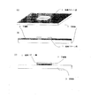
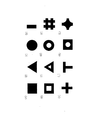
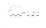
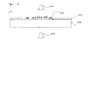
図1に平面形状が直方体である金属パターン層1を設けた標的物質検出素子用の基板の一例を示す。この標的物質検出素子用の基板は、支持体3の表面に設けられた下地層2上に孤立した金属パターン層(金属構造体)1が配置された構造を有する。なお、下地層2は、水と同等の屈折率を有する。図1(A)は基板表面の斜視図であり、図1(B)はその基板に垂直な方向での断面図である。下地層2は、図1(C)にあるように、金属パターン層1と同様にパターニングされていてもよい。図1(A)及び(B)に代表されるような構造が、最もシンプルな形態である。また、金属パターン層の二次元(平面)形状は、図2(A)乃至(L)に代表されるような形状をとることができる。製法上、外形と内形が同一の形状でない場合(図2(K))や、線状の金属パターン層の交差部が鋭角に形成されずに、丸く鈍ったような金属パターン層(図2(L))でもよい。これらの金属パターン層は、金、銀、銅、アルミニウム、白金のいずれかの金属、好ましくは貴金属、もしくはそれらの合金から構成され、下地層との密着性の観点から、これらの材質を選択することが好ましい。下地層としてフッ素を含有する材料で形成する場合には、下地層と金属層の間にクロムあるいはチタンなどの薄膜を形成してもよい。
(Substrate for target substance detection element)
A substrate for preparing a target substance detection element includes a support, and a metal pattern layer provided on the support via an underlayer having a refractive index equivalent to that of water. The shape (planar shape) and structure of the metal pattern layer can be appropriately determined according to the type of detection system. When applied to a detection system using the plasmon resonance method, the metal pattern layer is provided on the support as an isolated (independent) layer, or the metal layer on the support is provided with an opening (hole). Is preferred. Each of these preferred embodiments will be described below.
(1) Isolated Metal Pattern FIG. 1 shows an example of a substrate for a target substance detection element provided with a
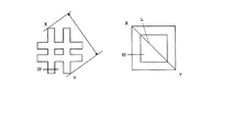
金属パターン層の平面形状における大きさ、すなわち、外周部における任意の一点から他の点までの距離は、10nm〜1450nmの範囲内にあることが好ましい。更には、50nm〜450nmの範囲内にあることが好ましい。この場合、任意の2点間の最大距離がこの範囲に入っていればよい、例えば、図13に示す井桁状のパターンの場合では点XY間の距離が最大であるので、この距離を上記の範囲内とする。また、図13に示す矩形リングパターンの場合でも、同様に外周形状のXY間の対角線Lの距離が最大であるのでLを上記の範囲内とする。図2(G)に示す円形リングパターンでは、外周円の直径を上記の範囲とする。金属パターン層1の平面形状の大きさがこの範囲にあることで、目的とする検出感度を達成できる局在プラズモン共鳴を更に効果的に得ることができる。
The size of the metal pattern layer in the planar shape, that is, the distance from an arbitrary point on the outer peripheral portion to another point is preferably in the range of 10 nm to 1450 nm. Furthermore, it is preferable that it exists in the range of 50 nm-450 nm. In this case, the maximum distance between any two points only needs to be within this range. For example, in the case of the cross-shaped pattern shown in FIG. 13, the distance between the points XY is the maximum. Within the range. Also in the case of the rectangular ring pattern shown in FIG. 13, the distance of the diagonal line L between the outer peripheral shapes XY is similarly the maximum, so L is within the above range. In the circular ring pattern shown in FIG. 2 (G), the diameter of the outer circumference circle is in the above range. When the size of the planar shape of the
一方、金属パターン層1を帯状の部分を有する構成とする場合、例えば図2(E)〜(L)の形状において、この帯状部分の幅(帯幅)は、本発明が目的とする局在プラズモン共鳴が得られるものであれば特に限定されない。帯幅は、10nm〜100nmの範囲とすることが好ましい。この帯幅は、例えば図2(G)の円形リングパターンの場合は、外周円と内周円の半径の差であり、また図13に示すパターンの場合では、Wで示される部分である。なお、帯状のパターンの幅は同一金属パターン層で同一であっても、帯幅に異なる部分があってもよい。
On the other hand, when the
金属パターン層は、必要に応じて基板上に1個以上を設ける。複数個設ける場合には、各金属パターン層の間隔(d)は、それを1つ支持体上に設けた際の吸収最大波長(λmax)を基準として、(λmax−50nm)≦d≦(λmax+50nm)の範囲から選択できる。具体的には、好ましくは50nm〜2000nm、より好ましくは400nm〜1500nmの範囲から選択した距離とすることよい。これは、金属パターン層同士のプラズモンによる相互作用により空間的な電場の分布・強度に影響があるためである。また、間隔が大きくなると、金属パターン層の密度が下がり、信号強度が弱くなってしまうため、特殊な光学系を適用する必要性が出てくるので、上記範囲にあることが好ましい。 One or more metal pattern layers are provided on the substrate as necessary. When a plurality of metal pattern layers are provided, the interval (d) between the metal pattern layers is (λmax−50 nm) ≦ d ≦ (λmax + 50 nm) with reference to the maximum absorption wavelength (λmax) when one metal pattern layer is provided on the support. ). Specifically, the distance is preferably selected from a range of 50 nm to 2000 nm, more preferably 400 nm to 1500 nm. This is because the spatial electric field distribution / intensity is affected by the plasmon interaction between the metal pattern layers. Moreover, since the density of a metal pattern layer will fall and signal intensity will become weak when a space | interval becomes large, it will be necessary to apply a special optical system, Therefore It is preferable to exist in the said range.
複数の金属パターン層を設ける場合は、平面形状及びその大きさの少なくとも一方において異なる複数種類の金属パターン層を基板上に設けることができる。金属パターン層の製造効率や検出系の構成を簡便化する点などを考慮した場合は、図3に示すように、数mm角程度の領域に同一形状及び大きさの金属パターン層1を規則的にアレイ状に支持体3上に配置することが好ましい。このような配置とすることで、透過光や散乱光、反射光の測定を容易にすることができる。
When a plurality of metal pattern layers are provided, a plurality of types of metal pattern layers that differ in at least one of the planar shape and the size thereof can be provided on the substrate. When considering the manufacturing efficiency of the metal pattern layer and the point of simplifying the configuration of the detection system, as shown in FIG. 3, the
金属パターン層の膜厚、外形、帯幅、隣接するもの同士の間隔は、局在プラズモン共鳴スペクトルのピーク位置に影響するため、測定に適したサイズに形成するものとするとよい。図2に示す各形状の中では、ループ部及び/または分岐部を有する形状が検出感度を更に向上させる上で好ましい。その理由としては以下の点が相乗的に影響していると考えられる。
(a)1つの金属パターン層における輪郭長さが増大すること。
(b)分岐部を利用する場合には更に角部の数が増加すること。
(c)金属パターン層の平面形状におけるエッジ間の距離を小さくできること。
Since the thickness, outer shape, band width, and distance between adjacent metal pattern layers affect the peak position of the localized plasmon resonance spectrum, they should be formed in a size suitable for measurement. Among the shapes shown in FIG. 2, a shape having a loop portion and / or a branch portion is preferable for further improving detection sensitivity. The reason is considered to be synergistically affected by the following points.
(A) The contour length in one metal pattern layer is increased.
(B) The number of corners further increases when a branching part is used.
(C) The distance between edges in the planar shape of the metal pattern layer can be reduced.
図1及び図2に示すような孤立した金属パターン(金属構造体)は、10nmから200nm程度の膜厚で形成することができる。
(2)開口型金属パターン層
図15に支持体表面に設けた金属層に開口を設けた金属パターン層の一例を示す。図15の平面図及び基板と垂直方向の断面図に示されるとおり、この基板における金属パターン層201は、支持体203上に下地層202を介して設けられている。金属パターン層201には多数の同一円形の開口が規則的に配列されている。この開口部は、金属パターン層の一部を下地層202が底部に露出するようにエッチング処理などを利用して除去することで形成することができる。図16は支持体302の屈折率を水と同等とした構成を示す。
An isolated metal pattern (metal structure) as shown in FIGS. 1 and 2 can be formed to a thickness of about 10 nm to 200 nm.
(2) Opening type metal pattern layer FIG. 15 shows an example of a metal pattern layer in which an opening is provided in the metal layer provided on the support surface. As shown in the plan view of FIG. 15 and the cross-sectional view in the direction perpendicular to the substrate, the
金属パターン層の有する開口部(ホール)の平面形状は、例えば、図17(a:微小スリット開口アレイ)及び(c:複合周期微小スリット開口アレイ)に示すような帯状とすることができる。更には、図17(b:微小開口2次元アレイ)に示すような短冊状、あるいは図17(d:微小開口2次元アレイ)に示すような三角形状など種々の形状とすることができる。金属層中に開口を複数設ける際には、異なる形状の開口が同一金属層に設けられていてもよい。しかしながら、製法上の利点を考慮すれば、同一形状の開口を規則的に配置することが好ましい。 The planar shape of the opening (hole) of the metal pattern layer can be, for example, a band shape as shown in FIGS. 17 (a: micro slit aperture array) and (c: compound periodic micro slit aperture array). Furthermore, various shapes such as a strip shape as shown in FIG. 17 (b: two-dimensional array of minute openings) or a triangle shape as shown in FIG. 17 (d: two-dimensional array of minute openings) can be used. When providing a plurality of openings in the metal layer, openings having different shapes may be provided in the same metal layer. However, considering the advantages of the manufacturing method, it is preferable to regularly arrange openings having the same shape.
また、この場合における金属パターン層も、金、銀、銅、アルミニウム、白金のいずれかの金属、好ましくは貴金属、もしくはそれらの合金から構成され、下地層との密着性の観点から、これらの材質を選択することが好ましい。下地層としてフッ素を含有する材料で形成する場合には、下地層と金属層の間にクロムあるいはチタンなどの薄膜を形成してもよい。 In this case, the metal pattern layer is also composed of any metal of gold, silver, copper, aluminum and platinum, preferably a noble metal, or an alloy thereof, and these materials are used from the viewpoint of adhesion to the underlayer. Is preferably selected. When the underlayer is formed of a material containing fluorine, a thin film such as chromium or titanium may be formed between the underlayer and the metal layer.
この場合における金属パターン層の厚さも、10nmから200nm程度の膜厚で形成することができ、照射光の波長帯域で適宜選択して用いられる。例えばAuの場合だと、50nm程度が好ましい。パターンの形状については、金属の自由電子と相互作用してくる光が主な成分となるパターン形状であることが好ましく、膜に複数の開口を有する形状が好ましい。開口の断面形状は円形、楕円形、三角形、矩形、多角形など種々の形態をとりえる。 The thickness of the metal pattern layer in this case can also be formed with a film thickness of about 10 nm to 200 nm, and is appropriately selected depending on the wavelength band of the irradiation light. For example, in the case of Au, about 50 nm is preferable. The shape of the pattern is preferably a pattern shape in which light interacting with metal free electrons is a main component, and a shape having a plurality of openings in the film is preferable. The cross-sectional shape of the opening can take various forms such as a circle, an ellipse, a triangle, a rectangle, and a polygon.
複数の開口を設ける場合の隣接する2つの開口間の距離は、照射光の波長以下の距離として所望とする検出系に応じて選択することが好ましい。この開口間の距離は、先に説明した孤立型の金属パターン間の距離と同様にして設定することができる。 The distance between two adjacent openings when providing a plurality of openings is preferably selected according to a desired detection system as a distance equal to or less than the wavelength of the irradiation light. The distance between the openings can be set in the same manner as the distance between the isolated metal patterns described above.
(下地層)
下地層は水と同等の屈折率を有する材料からなる。この材料としては、透明な低誘電率素材を用いることが望ましい。このような材料には無機材料や有機材料がある。無機材料としては、フッ化マグネシウム(屈折率:1.37)またはフッ化リチウム(屈折率:1.39)を挙げることができる。
(Underlayer)
The underlayer is made of a material having a refractive index equivalent to that of water. As this material, it is desirable to use a transparent low dielectric constant material. Such materials include inorganic materials and organic materials. Examples of the inorganic material include magnesium fluoride (refractive index: 1.37) or lithium fluoride (refractive index: 1.39).
有機材料としては各種のポリマーを挙げることができる。 Examples of the organic material include various polymers.
下地層を形成するための材料としては、フッ素を含有する材料が好ましい。フッ素を含む有機材料としては、フッ素樹脂が好ましい。更に、透明性や屈折率などの光学特性上の観点から非晶質構造をとるフッ素樹脂(例えば、PTFE(ポリテトラフルオロエチレン、屈折率:1.35))がより好ましい。このようなフッ素樹脂として具体的には、サイトップ(旭硝子(株)製)、テフロンAF(デュポン社製)などのいずれか、もしくはそれらの混合物を挙げることができる。 As a material for forming the underlayer, a material containing fluorine is preferable. As the organic material containing fluorine, a fluororesin is preferable. Furthermore, a fluororesin having an amorphous structure (for example, PTFE (polytetrafluoroethylene, refractive index: 1.35)) is more preferable from the viewpoint of optical properties such as transparency and refractive index. Specific examples of such a fluororesin include Cytop (manufactured by Asahi Glass Co., Ltd.), Teflon AF (manufactured by DuPont), or a mixture thereof.
本発明においては、標的物質が含まれる水(屈折率:1.34)と同程度の屈折率をもつ下地層を備えることにより金属パターン層は同程度の屈折率をもつ材料に囲まれた状態となる。これにより異なる屈折率層(誘電体層)からの反射が抑制され、プラズモン共鳴の乱れが抑制されてプラズモン共鳴ピークがシャープなものとなる。 In the present invention, the metal pattern layer is surrounded by a material having the same refractive index by providing the base layer having the same refractive index as water (refractive index: 1.34) containing the target substance. It becomes. Thereby, reflection from different refractive index layers (dielectric layers) is suppressed, turbulence of plasmon resonance is suppressed, and the plasmon resonance peak becomes sharp.
下地層の厚さは、支持体を兼ねる場合などのその形態に応じて適宜選択できる。別途設けた支持体上に下地層を設ける場合(例えば後述する支持体の形態(II)の場合など)には、好ましくは10nm以上50μm以下、より好ましくは100nm以上、30μm以下とすることができる。 The thickness of the underlayer can be appropriately selected depending on the form of the base layer. When a base layer is provided on a separately provided support (for example, in the case of the form (II) of the support described later), it is preferably 10 nm to 50 μm, more preferably 100 nm to 30 μm. .
下地層の屈折率は、一般に顕微分光測光装置を用いた分光反射率や透過率から屈折率を求める方法と, エリプソメトリーによる方法によって定義されるものとする。 The refractive index of the underlayer is generally defined by a method for obtaining a refractive index from spectral reflectance and transmittance using a microspectrophotometer and a method by ellipsometry.
(支持体)
下地層及び金属パターン層が設けられる支持体は、これらの層を支持し、かつこれらの層をも用いた標的物質の検出を可能とするものであればよい。また、支持体自体が下地層を兼ねる構成でもよく、支持体上に複数の層を形成し、その最上層を下地層として利用してもよい。このような構成としては以下の各態様を挙げることができる。
(I)支持体が単一の層から構成されており、下地層としての機能を有する。
(II)支持体上に下地層を有する。
(Support)
The support on which the underlayer and the metal pattern layer are provided may be any support that supports these layers and enables detection of a target substance using these layers. Further, the support itself may also serve as an underlayer, or a plurality of layers may be formed on the support, and the uppermost layer may be used as the underlayer. Examples of such a configuration include the following aspects.
(I) The support is composed of a single layer and functions as an underlayer.
(II) An underlayer is provided on the support.
上記の(II)の形態において用い得る支持体としては、光学的に透明なガラス板、石英板、ポリカーボネートやポリスチレンなどの樹脂板などを挙げることができる。また、(I)の形態の下地層としての機能も兼ねる支持体としては、水と同等の屈折率を有するフッ素樹脂からなる板が好適に用いられる。 Examples of the support that can be used in the form (II) include an optically transparent glass plate, a quartz plate, and a resin plate such as polycarbonate and polystyrene. In addition, as the support that also serves as the base layer in the form (I), a plate made of a fluororesin having a refractive index equivalent to that of water is preferably used.
(基板の作製方法)
(i)孤立型金属パターン層
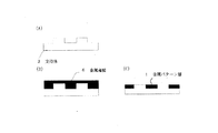
孤立型の金属パターン層の形成方法の一例を図面を用いて説明する。図5に示したように、まず、支持体上に、下地層形成用の材料を用いて下地層を成膜する(図5(B))。樹脂を用いる場合は、スピンコート法などを用いる。また、無機材料の場合は蒸着法などが利用できる。続いて金属薄膜をスパッタ法あるいは蒸着法により成膜する(図5(C))。その上に電子線レジストをスピンコートにより成膜し(図5(D))、電子線描画装置で露光し、現像後レジストパターンを得る(図5(E))。その後、不要な金属薄膜をエッチングし(図5(F))、レジストを除去して、フッ素を含有する材料を下地に持った、アレイ状の金属パターン層を形成する(図5(G))。前述の電子線描画装置の他、集束イオンビーム加工装置、X線露光装置、EUV露光装置によるパターニング法で金属パターン層を成形することもできる。
(Manufacturing method of substrate)
(I) Isolated metal pattern layer An example of a method for forming an isolated metal pattern layer will be described with reference to the drawings. As shown in FIG. 5, first, a base layer is formed on the support using a material for forming the base layer (FIG. 5B). When using a resin, a spin coat method or the like is used. In the case of an inorganic material, a vapor deposition method or the like can be used. Subsequently, a metal thin film is formed by sputtering or vapor deposition (FIG. 5C). An electron beam resist is formed thereon by spin coating (FIG. 5D), and is exposed by an electron beam drawing apparatus to obtain a resist pattern after development (FIG. 5E). Thereafter, unnecessary metal thin film is etched (FIG. 5F), the resist is removed, and an array-shaped metal pattern layer having a fluorine-containing material as a base is formed (FIG. 5G). . In addition to the electron beam lithography apparatus described above, the metal pattern layer can be formed by a patterning method using a focused ion beam processing apparatus, an X-ray exposure apparatus, or an EUV exposure apparatus.
また、図6に示したように、フッ素樹脂材料を用いて、モールド法により作製した微細な凹凸を有する支持体(図6(A))を用いた作製方法も可能である。図6にあるように、支持体の凹凹凸形成面上に金属薄膜をスパッタ法あるいは蒸着法により成膜する(図6(B))。次に、表面の金属薄膜を研磨し、所望の層構造を有する金属の構造体を基板上に形成する(図6(C))。図7は、金属パターン層の厚さが凹凸の高さよりも薄い場合の作製方法を示すものである。この場合、支持体の凸部が金属パターン層のより上部にあってもよいし、凹凸部の壁面に金属薄膜が成膜されていてもよい。ここで、研磨する代わりに金属膜をドライエッチングによるエッチバックを利用して除去することも可能である。 Further, as shown in FIG. 6, a manufacturing method using a support body (FIG. 6A) having fine unevenness manufactured by a molding method using a fluororesin material is also possible. As shown in FIG. 6, a metal thin film is formed on the concave / convex formation surface of the support by sputtering or vapor deposition (FIG. 6B). Next, the metal thin film on the surface is polished to form a metal structure having a desired layer structure on the substrate (FIG. 6C). FIG. 7 shows a manufacturing method when the thickness of the metal pattern layer is thinner than the height of the unevenness. In this case, the convex portion of the support may be located above the metal pattern layer, or a metal thin film may be formed on the wall surface of the concave and convex portion. Here, instead of polishing, the metal film can be removed by using etch back by dry etching.
(ii)開口型金属パターン層
基本的には、上記した孤立型金属パターン層と同様にして作製可能である。すなわち、図5の(A)〜(D)に示すように、支持体上に、下地層、金属層及びレジスト層をこの順に設け、開口に相当する位置にあるレジスト層の部分を除去して、レジストパターンを形成し、このレジストパターンを介して金属層をエッチングすることで、開口型金属パターン層を得ることができる。
(Ii) Opened metal pattern layer Basically, it can be produced in the same manner as the above-described isolated metal pattern layer. That is, as shown in FIGS. 5A to 5D, an underlayer, a metal layer, and a resist layer are provided in this order on a support, and a portion of the resist layer at a position corresponding to the opening is removed. An opening type metal pattern layer can be obtained by forming a resist pattern and etching the metal layer through the resist pattern.
(標的物質検出用素子及び標的物質)
上記の各種の構成をとり得る基板の金属パターン層に標的物質捕捉体を結合させることで標的物質検出素子を作製することができる。図4及び図15に標的捕捉体を金属パターン層に固定した状態を示す。
(Target substance detection element and target substance)
The target substance detection element can be produced by binding the target substance capturing body to the metal pattern layer of the substrate that can take the above-described various configurations. 4 and 15 show a state where the target capturing body is fixed to the metal pattern layer.
標的物質としては、標的物質捕捉体と特異的な結合対を形成するものであれば、特に制約はない。具体的には、試料溶液中に含まれる標的物質は、非生体物質と生体物質に大別される。非生体物質として産業上利用価値の大きいものとしては、環境汚染物質としての塩素置換数/位置の異なるPCB類、同じく塩素置換数/位置の異なるダイオキシン類、いわゆる環境ホルモンと呼ばれる内分泌撹乱物質等が挙げられる。生体物質としては、核酸、タンパク質、糖鎖、脂質及びそれらの複合体から選択される。更に詳しくは、核酸、タンパク質、糖鎖、脂質から選択される生体分子を含んでなるものがある。具体的には、DNA、RNA、アプタマー、遺伝子、染色体、細胞膜、ウイルス、抗原、抗体、レクチン、ハプテン、ホルモン、レセプター、酵素、ペプチド、スフィンゴ糖、スフィンゴ脂質などを挙げることができる。更には、前記の「生体物質」を産生する細菌や細胞そのものも、本発明が対象とする「生体物質」として標的物質となり得る。 The target substance is not particularly limited as long as it forms a specific binding pair with the target substance capturing body. Specifically, the target substance contained in the sample solution is roughly classified into a non-biological substance and a biological substance. Industrially valuable non-biological substances include PCBs with different chlorine substitution numbers / positions as environmental pollutants, dioxins with different chlorine substitution numbers / positions, endocrine disrupting substances called so-called environmental hormones, etc. Can be mentioned. The biological material is selected from nucleic acids, proteins, sugar chains, lipids, and complexes thereof. More specifically, there are those comprising a biomolecule selected from nucleic acids, proteins, sugar chains, and lipids. Specific examples include DNA, RNA, aptamer, gene, chromosome, cell membrane, virus, antigen, antibody, lectin, hapten, hormone, receptor, enzyme, peptide, sphingosaccharide, sphingolipid and the like. Furthermore, bacteria and cells themselves that produce the above-mentioned “biological substances” can also be target substances as “biological substances” targeted by the present invention.
標的物質捕捉体としては、上記の標的物質に対して特異的に結合し得るものが利用される。例えば、標的物質と標的物質捕捉体との関係が、酵素−基質、抗原−抗体、核酸−核酸、化合物−その受容体、化合物−それに対して特異的な親和性を有する物質などである場合の一方を標的物質捕捉体として他方を標的物質することができる。これらの捕捉体は、物理的あるいは化学的な方法により、金属パターン層の表面に固定化できる。 As the target substance capturing body, a substance capable of specifically binding to the target substance is used. For example, when the relationship between the target substance and the target substance capturing body is enzyme-substrate, antigen-antibody, nucleic acid-nucleic acid, compound-its receptor, compound-substance having specific affinity for it, etc. One can be a target substance capturing body and the other can be a target substance. These capturing bodies can be immobilized on the surface of the metal pattern layer by a physical or chemical method.
図4及び図15は標的物質捕捉体5、204として抗体を用いた場合を示している。抗体を金属パターン層1、201に固定すると、金属パターン層1、201に標的物質(4)が近づくと特異的に複合体が形成される。その結果、検出素子表面における誘電率(屈折率)が変化する。前記抗体とは、任意の免疫グロブリンクラスのメンバーであり、本発明においては、IgGクラスの誘導体がより好ましい。また、捕捉体としての抗体は、任意の手法により断片化された抗体フラグメント(抗体断片)でもよい。前記抗体フラグメントあるいは抗体断片とは、前記抗体あるいは免疫グロブリンの全長に満たない抗体の任意の分子あるいは複合体をいう。好ましくは、抗体フラグメントは、少なくとも、全長抗体の特異的結合能力の重要な部分を保持する。抗体フラグメントの例としては、Fab、Fab'、F(ab')2、scFv、Fv、多重特異性多価抗体(ディアボディー、トライアボディなど)およびFdフラグメントが挙げられるがこれらに限定されるものではない。抗体フラグメントを用いる場合、より検出素子近傍での捕捉が可能であるため、検出感度を向上することができる。また、多重特異性多価抗体を用いる場合、検出素子と標的物質の各々に対して特異的認識能を有するので、簡便かつ効率的に検出素子上に捕捉体を固定化することができる。このような複合体形成における抗原抗体反応以外の例としては、酵素と基質の複合体、DNAのハイブリダイゼーションによる相補的な塩基対形成などが挙げられ、これらの複合体の一方を他方の捕捉体として利用することができる。
4 and 15 show a case where an antibody is used as the target
これらの捕捉体は、物理的あるいは化学的な方法により、検出素子の表面に固定化される。なお、検出素子の表面は、いわゆる非特異吸着による共雑物の吸着による不必要なシグナルを防止するために、スキムミルクやカゼイン、ウシ血清アルブミン、リン脂質、ポリエチレングリコール及びそれらの誘導体などによるコーティングを行うと、なお好適である。 These capturing bodies are immobilized on the surface of the detection element by a physical or chemical method. In addition, the surface of the detection element is coated with skim milk, casein, bovine serum albumin, phospholipid, polyethylene glycol, and derivatives thereof to prevent unnecessary signals due to adsorption of contaminants due to so-called non-specific adsorption. It is still preferred to do so.
本発明にかかる標的物質検出用素子では、下地層の屈折率が、試料溶液に含まれる水と同等の屈折率を有するので、入射光が下地層により反射されにくくなることにより金属パターン層と入射光との相互作用の結果のみを抽出できること、及び、孤立型の金属パターン層の場合には、隣接する金属パターン層の間隔を共鳴波長に近づけた構成を採用することにより、回折現象の影響による、隣接する金属パターン層同士によるコヒーレントな局在プラズモンの相互作用を得ることができる。その結果、より鋭いピーク波形が得られ、スペクトルシフトをより敏感に検出できる。これにより、試料溶液中の微量の標的物質を検出することができる検出素子及びそれを用いた標的物質の検出方法、並びにそのための検出装置及びキットを提供することができる。 In the target substance detection element according to the present invention, the refractive index of the underlayer has the same refractive index as that of water contained in the sample solution. It is possible to extract only the result of interaction with light, and in the case of an isolated metal pattern layer, by adopting a configuration in which the interval between adjacent metal pattern layers is close to the resonance wavelength, Coherent localized plasmon interaction between adjacent metal pattern layers can be obtained. As a result, a sharper peak waveform can be obtained and the spectral shift can be detected more sensitively. Thereby, the detection element which can detect the trace amount target substance in a sample solution, the detection method of the target substance using the same, and the detection apparatus and kit for it can be provided.
また、開口型金属パターン層を用いた場合には、開口を透過してくる透過光の強度変化を更に増幅させることが可能となり、試料溶液中の標的物質を検出するに十分な感度と広いダイナミックレンジを達成することが可能となる。 In addition, when an aperture-type metal pattern layer is used, it is possible to further amplify changes in the intensity of transmitted light that passes through the aperture, and sufficient sensitivity and wide dynamics to detect the target substance in the sample solution A range can be achieved.
本発明は、プラズモン共鳴が元来より有している、反応中の経時的変化検知のメリットを保ったまま、上述した種々の効果を発揮可能である。 The present invention can exhibit the various effects described above while maintaining the merit of detecting change over time during the reaction, which plasmon resonance originally has.
(検出装置及び検出方法)
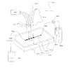
次に、上記の構成の素子を用いた標的物質検出装置について説明する。本発明による検出装置は、上記構成の素子を保持する保持手段と、素子からの信号を検出するための検出手段と、を少なくとも有して構成される。本発明による検出装置の一例を図8に示す。検出手段としては、光源と分光器、レンズ類から構成される光学検出系を有する。また、この装置では、試料溶液を検出素子まで移動させ素子との反応を起させるための、反応用ウェル、流路、送液機構等からなる送液系を更に有する。
(Detection apparatus and detection method)
Next, a target substance detection apparatus using the element configured as described above will be described. The detection apparatus according to the present invention includes at least holding means for holding the element having the above-described configuration and detection means for detecting a signal from the element. An example of a detection device according to the present invention is shown in FIG. The detection means includes an optical detection system including a light source, a spectroscope, and lenses. In addition, this apparatus further includes a liquid feeding system including a reaction well, a channel, a liquid feeding mechanism, and the like for moving the sample solution to the detection element and causing a reaction with the element.
光源としては、可視領域から近赤外領域までの波長領域をカバーできるものを用いることができる。光学測定は、吸収スペクトル、透過スペクトル、散乱スペクトル、反射スペクトルを用いることができる。最も好ましくは、吸収スペクトルのピーク波長あるいは、ピークの吸収強度を利用する。 As a light source, what can cover the wavelength range from a visible region to a near infrared region can be used. The optical measurement can use an absorption spectrum, a transmission spectrum, a scattering spectrum, and a reflection spectrum. Most preferably, the peak wavelength of the absorption spectrum or the peak absorption intensity is used.
孤立型金属パターン層を有する検出素子では、標的物質を特異的に結合すると、局在プラズモン共鳴が非結合状態に対して変化し、吸収スペクトルのピーク波長は、長波長側にシフトし、同時に吸収強度は増大する。そのシフト量の程度によって、あらかじめ作成しておいた標的物質に対する検量線から標的物質の量を定量することができる。また、前記透過光と同様に反射光、散乱光によっても検出定量可能である。図示した検出装置は、局在プラズモン共鳴を利用しているので、孤立型金属パターン層近傍では、局所的な電場増強が起こる。この現象は、表面増強ラマン分光法(SERS)や表面プラズモン蛍光分光法(SPFS)などの測定法にも応用でき、これらの方法による標的物質の定量も可能である。 In the detection element having an isolated metal pattern layer, when the target substance is specifically bound, the localized plasmon resonance changes with respect to the unbound state, and the peak wavelength of the absorption spectrum shifts to the longer wavelength side and absorbs at the same time. Strength increases. Depending on the degree of the shift amount, the amount of the target substance can be determined from a calibration curve for the target substance prepared in advance. Further, detection and quantification can be performed by reflected light and scattered light as well as the transmitted light. Since the illustrated detection apparatus utilizes localized plasmon resonance, local electric field enhancement occurs in the vicinity of the isolated metal pattern layer. This phenomenon can be applied to measurement methods such as surface-enhanced Raman spectroscopy (SERS) and surface plasmon fluorescence spectroscopy (SPFS), and the target substance can be quantified by these methods.
反応用ウェルや流路は、いわゆるμTAS(Micro Total Analysis Systems)型の装置で用いられているポリジメチルシロキサン(PDMS)基板を利用すると容易に作製可能である。このPDMS基板を検出素子を作製してある基板と貼りあわせて図8のような形状にて使用するものとする。送液機構としては、マイクロピストンポンプやシリンジポンプなどを用いることができる。 The reaction well and the flow path can be easily produced by using a polydimethylsiloxane (PDMS) substrate used in a so-called μTAS (Micro Total Analysis Systems) type apparatus. This PDMS substrate is bonded to the substrate on which the detection element is manufactured and used in the shape as shown in FIG. As a liquid feeding mechanism, a micro piston pump, a syringe pump, or the like can be used.
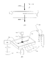
次に、代表的な使用形態を図9に示す。まず、捕捉能を持つ検出素子10のある反応ウェル部9に標的物質を含む試料溶液を流路8を介して送液ポンプ18でインレット11より導入する。一定時間のインキュベーションを行い、その時の透過スペクトルを分光光度計15により測定する。中央演算装置16にて、あらかじめ作成してある検量線と比較し、濃度や反応速度などの測定結果を表示ユニット17に表示する。必要があれば、測定前にリン酸緩衝液などを洗浄液としてインレット1より導入し、反応ウェル部9を洗浄してもよい。ここで、一定時間後のスペクトル変化を静的に測定する他に、その変化を動的にリアルタイム測定することも可能である。その場合、時間変化率などを新たな情報として取得することができる。
Next, a typical usage pattern is shown in FIG. First, a sample solution containing a target substance is introduced from an inlet 11 through a flow path 8 into a
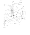
開口型金属パターンを用いた素子に対して透過光を測定する形態の装置を図14に示す。光源101としては、安定した光源であれば特に制限はない。例えば、ハロゲンランプを用いることが好ましい。受光手段102としては、1nm程度の波長分解能をもった分光計測装置が望ましい。例えば、マルチチャネル検出器や分光光度計を用いることが好ましい。試料溶液リザーバー103としては、標的物質の非特異吸着が少ない材料で構成させたリザーバー、もしくは、チップ中にリザーバーを作り込んだ構成のものでもかまわない。例えば、非特異吸着防止コーティングしたエッペンドルフチューブを用いることが好ましい。洗浄液リザーバー104としては、特に制限はない。ここでは、生化学用のガラスもしくはプラスチックチューブを用いることが好ましい。流路切り替えバルブ105としては、流体のチューブを切り替えられれば特に制限はない。例えば、三方向バルブを用いることが好ましい。送液手段106としては、シリンジポンプやチューブポンプ、ダイヤフラムポンプなどを適宜選択して用いることができる。廃液タンク107としては、ポンプにシリンジポンプを使用した場合、シリンジがそのまま廃液タンクになる。チューブポンプやダイヤフラムポンプを用いた場合は、ビーカーや瓶を廃液タンクとして用いることができる。また、試料溶液が少量しかない場合は廃液にせず、循環用の流路やチューブを用い試料溶液を循環させてやってもよい。送液および廃液チューブ108、109としては、標的物質の吸着ができる限り少ない材質のチューブが好ましい。標的物質検出素子110としては、図15〜17に示す素子が、適宜選択して使用される。流路111としては、試料溶液量ができる限り減らすことができるよう微小なものであることが好ましい。また、流路表面に標的物質ができる限り吸着しないようコーティングが施されていることが好ましい。カバー112としては、透明な材料でかつ、基板113とともに流路を形成でき得る材料であることが好ましい。
FIG. 14 shows an apparatus for measuring transmitted light with respect to an element using an aperture type metal pattern. The
次に、上記の開口型金属パターンを用いた素子を用いた検出装置の動作原理を図15及び図22を用いて説明する。図15において、図中、上方向から下方向(+z方向)に向かって入射光205を微小開口201の配列に入射させる。このとき、開口の大きさと間隔は、ともに、検出に用いる光の波長以下であるため、入射光205の電界のうち、図中のx方向に偏光した成分が金属薄膜201中の電子と相互作用し、微小スリット開口の内側面に表面プラズモンを生じさせる。生じた表面プラズモンは微小スリット内側面を下方向(図中の+z方向)に伝搬し、微小開口201の下端で再び光に変換され、透過光206として、下方向(+z方向)に透過する。
Next, the principle of operation of the detection device using the element using the aperture type metal pattern will be described with reference to FIGS. In FIG. 15,
複数の微小開口201内を表面プラズモンの状態を経て光が透過する際、微小開口に生じる電気多重極子との共鳴(局在プラズモン共鳴)による吸収を受け、入射光の波長変化に対するスペクトルは、特徴的な共鳴ピークを持つ。この局在プラズモン共鳴ピークの形は、微小開口の幅や間隔によって変化する。
When light is transmitted through the plurality of
この開口型金属パターンを有する素子では、微小開口を有する金属薄膜の下地層として、標的物質を含む試料溶液の液媒体である水と同程度の屈折率を有する下地層が配置されていることにより、入射光がプラズモンを介して効率よく透過光に変換される。本構成により、標的物質が捕捉体と結合したとき、透過光の積分強度の変化が大きくなる。 In the element having the opening-type metal pattern, a base layer having a refractive index comparable to that of water, which is a liquid medium of a sample solution containing a target substance, is disposed as a base layer of a metal thin film having a minute opening. Incident light is efficiently converted into transmitted light via plasmons. With this configuration, when the target substance is bound to the capturing body, the change in the integrated intensity of the transmitted light is increased.
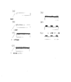
この開口型金属パターンを有する素子を配置した検出装置で得られる透過光強度スペクトルの一例を図22に示す。(a)は下地層と水の屈折率が同等でない場合の透過光スペクトルであり、(b)は下地層と水の屈折率が同等である場合の透過光スペクトルである。図より、水と下地層の屈折率を同等にした場合は、透過光スペクトルの積分強度変化が大きくなっていることが分かる。図23は、さまざまな濃度の検体を一定時間反応させた後、素子表面を緩衝溶液で洗浄したあとの信号強度変化を示した図であり、(b)は(a)よりも検出限界が低くかつダイナミックレンジが大きいことが確認できる。点線は、標的物質が補足分子と反応を起こす前のスペクトルを表す。図15に示した素子を、標的物質を含む検体と接触させ、素子と標的物質を反応させる。反応時間に応じて、透過光スペクトルの積分強度は大きくなっていく。この積分強度の時間変化を示したグラフが、図20であり、本発明で示した構成のセンサを用いることで、標的物質と抗体の反応ダイナミクスを観測することが可能となる。 FIG. 22 shows an example of a transmitted light intensity spectrum obtained by a detection device in which an element having this aperture type metal pattern is arranged. (A) is a transmitted light spectrum when the refractive index of a foundation layer and water is not equivalent, (b) is a transmitted light spectrum when the refractive index of a foundation layer and water is equivalent. From the figure, it can be seen that when the refractive indices of water and the underlayer are made equal, the change in the integrated intensity of the transmitted light spectrum increases. FIG. 23 is a diagram showing a change in signal intensity after reacting specimens of various concentrations for a certain period of time and then washing the element surface with a buffer solution, and (b) shows a lower detection limit than (a). And it can be confirmed that the dynamic range is large. The dotted line represents the spectrum before the target substance reacts with the complementary molecule. The element shown in FIG. 15 is brought into contact with a specimen containing a target substance, and the element and the target substance are reacted. Depending on the reaction time, the integrated intensity of the transmitted light spectrum increases. A graph showing the change in the integrated intensity with time is shown in FIG. 20, and the reaction dynamics between the target substance and the antibody can be observed by using the sensor having the configuration shown in the present invention.
標的物質の有無またはその量の検出を行う試料溶液は、水溶液として供給される。水溶液は、水を溶媒(液媒体)として構成されたものである。溶解している溶質としては、主にタンパク質や塩類(リン酸塩、酢酸塩、ホウ酸塩、トリス塩酸塩、塩化物塩、カルシウム塩、マグネシウム塩など)などが含まれる。また、糖類(トレハロースなど)やグリセロールやエチレングリコールなどの凍結保護剤、アジ化ナトリウムやチメロサールなどの防腐剤、PMSF(フェニルメタンスルホニルフルオライド)やロイペプチンのようなプロテアーゼ阻害剤、EDTA(エチレンジアミン四酢酸二ナトリウム,エチレンジアミンテトラ酢酸二ナトリウム)などの金属キレート剤、DTT(ジチオスレイトール)などの還元剤を含んでいてもよい。 A sample solution for detecting the presence or absence of the target substance or its amount is supplied as an aqueous solution. The aqueous solution is composed of water as a solvent (liquid medium). The dissolved solute mainly includes proteins and salts (phosphate, acetate, borate, tris hydrochloride, chloride salt, calcium salt, magnesium salt, etc.). In addition, saccharides (such as trehalose), cryoprotectants such as glycerol and ethylene glycol, preservatives such as sodium azide and thimerosal, protease inhibitors such as PMSF (phenylmethanesulfonyl fluoride) and leupeptin, EDTA (ethylenediaminetetraacetic acid) A metal chelating agent such as disodium or disodium ethylenediaminetetraacetate) or a reducing agent such as DTT (dithiothreitol) may be included.
(検出用キット)
本発明の標的物質検出用のキットとしては、以下のような種々の形態で提供することができる。
(I)標的物質検出素子用の基板と、標的物質捕捉体と、を有する標的物質検出用キット。
(II)標的物質検出素子と、検出装置と、標的物質の前記標的物質検出素子での捕捉に必要な試薬と、を有する標的物質検出用キット。
(Detection kit)
The target substance detection kit of the present invention can be provided in the following various forms.
(I) A target substance detection kit having a substrate for a target substance detection element and a target substance capturing body.
(II) A target substance detection kit comprising a target substance detection element, a detection device, and a reagent necessary for capturing the target substance by the target substance detection element.
上記の(II)の構成のキットを用いることで本発明にかかる標的物質の検出を行うことができる。上記の(I)の構成のキットによれば、検出装置や試薬を既に有している使用者に、新たな標的物質検出素子を提供することができる。 The target substance according to the present invention can be detected by using the kit having the constitution (II). According to the kit having the above configuration (I), a new target substance detection element can be provided to a user who already has a detection device and a reagent.
以下、本発明を実施例により更に具体的に説明する。なお、本発明は以下の実施例のみに限定されるものではない。 Hereinafter, the present invention will be described more specifically with reference to examples. In addition, this invention is not limited only to a following example.
実施例1
図10に本実施例で用いた概略の構造を示す。ここでは、まず、625μm厚の石英基板上に室温で5%Cytop溶液(CTL−809M(旭硝子(株)製))(溶媒:CTL−180(旭硝子(株)製)をスピンコートする。2500rpmで45秒間保持することで、膜厚500nmを得る。70℃40分、続けて190℃1時間のベークを行い、フッ素樹脂層を形成する。次に、膜厚20nmの金の薄膜をスパッタ法により石英基板上のフッ素樹脂層上に成膜する。
Example 1
FIG. 10 shows a schematic structure used in this example. Here, first, a 5% Cytop solution (CTL-809M (Asahi Glass Co., Ltd.)) (solvent: CTL-180 (Asahi Glass Co., Ltd.)) is spin-coated on a 625 μm thick quartz substrate at 2500 rpm. Holding for 45 seconds gives a film thickness of 500 nm, followed by baking at 70 ° C. for 40 minutes, followed by baking at 190 ° C. for 1 hour, to form a fluororesin layer. A film is formed on the fluororesin layer on the quartz substrate.
金薄膜上のネガ型電子線レジスト(SAL601(ローム&ハース社製))をスピンコートし、電子線描画装置によりパターニングする。そして、レジストをマスクとして金薄膜をパターニングし、孤立型金属パターン層を形成させる。各金属パターン層は200nm×200nmのスクエアパターン(平面形状)である。隣接する金属パターン層間の間隔は800nmであり、多数の金属パターン層が規則的なアレイ状に3mm×3mmの領域に配置されている。 A negative electron beam resist (SAL601 (made by Rohm & Haas)) on a gold thin film is spin-coated and patterned by an electron beam drawing apparatus. Then, the gold thin film is patterned using the resist as a mask to form an isolated metal pattern layer. Each metal pattern layer is a 200 nm × 200 nm square pattern (planar shape). An interval between adjacent metal pattern layers is 800 nm, and a large number of metal pattern layers are arranged in a 3 mm × 3 mm region in a regular array.
次に、金属パターン層表面に捕捉能を付与するため、標的物質捕捉体である抗AFP(α−fetoprotein)抗体を金からなる金属パターン層表面に固定する。まず、金と親和性の高いチオール基を持つ、11−Mercaptoundecanoic acidのエタノール溶液をスポッタ等で滴下し、金属パターン層表面を修飾する。これにより、金属パターン層表面にカルボキシル基が露出される。その状態で、N−Hydroxysulfosuccinimide(同仁化学研究所社製)水溶液と1−Ethyl−3−[3−dimethylamino]propyl]carbodiimide hydrochloride(同仁化学研究所社製)水溶液を同様にスポッタにて反応領域に滴下する。これにより、金属パターン層表面にスクシンイミド基が露出される。さらに、ストレプトアビジンを結合させることにより、金属パターン層表面がストレプトアビジンで修飾される。この金属パターン層にビオチン化した抗AFP抗体を固定させる。 Next, an anti-AFP (α-fetoprotein) antibody, which is a target substance capturing body, is immobilized on the surface of the metal pattern layer made of gold in order to impart a capture capability to the surface of the metal pattern layer. First, an ethanol solution of 11-Mercaptodecanoic acid having a thiol group having a high affinity for gold is dropped with a spotter or the like to modify the surface of the metal pattern layer. Thereby, the carboxyl group is exposed on the surface of the metal pattern layer. In this state, an aqueous solution of N-Hydroxysulfuccinimide (manufactured by Dojindo Laboratories) and an aqueous solution of 1-Ethyl-3- [3-dimethylamino] propyl] carbohydrate hydride (manufactured by Dojindo Laboratories) are similarly applied to the reaction region using a spotter. Dripping. Thereby, the succinimide group is exposed on the surface of the metal pattern layer. Further, by binding streptavidin, the surface of the metal pattern layer is modified with streptavidin. A biotinylated anti-AFP antibody is immobilized on the metal pattern layer.
多数の金属パターン層を有する領域の複数を基板上に作製し、それぞれに異なる抗体を固定させ、試料溶液中の異なる標的物質を同一基板上にて検出するような構成(マルチセンサ構成)をとることも可能である。この場合、異なる抗体を用いて、前記の方法と同様の固定化操作を各領域ごとに行うことでかかる構成を得ることができる。 A plurality of regions having a large number of metal pattern layers are prepared on a substrate, different antibodies are immobilized on each of them, and different target substances in a sample solution are detected on the same substrate (multi-sensor configuration). It is also possible. In this case, such a configuration can be obtained by performing different immobilization operations for each region using different antibodies.
以上のようにして得られる素子を用いて以下の操作により、特異的に試料溶液中のAFP濃度を測定することができる。 Using the element obtained as described above, the AFP concentration in the sample solution can be specifically measured by the following operation.
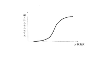
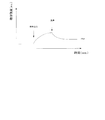
まず、作製した素子10に標的物質であるAFPを含んだ試料溶液をインレット11より導入し、AFPを構造体上に捕捉させる。試料溶液をアウトレット12より排出し、次に、リン酸緩衝液をインレット11より導入し、反応ウェル9内部を洗浄する。最後にリン酸緩衝液を充填して、金の金属パターン層の吸収スペクトルを測定する。吸収スペクトルは、図11に一例を示すように、反応前と反応後を比較すると、特異的な抗原抗体反応によって、標的物質が検出素子表面に結合することでシフトする。ここで、吸収スペクトルのピーク強度、あるいはピーク波長のシフト量とAFP濃度の相関は、図12の検量線の様にあらかじめ既知のAFPコントロール溶液により求められており、これにより濃度未知の試料溶液の微量AFP濃度を求めることができる。
First, a sample solution containing AFP, which is a target substance, is introduced from the inlet 11 into the manufactured element 10 to capture AFP on the structure. The sample solution is discharged from the
実施例2
本実施例では、フッ素樹脂基板を用いてモールド法により微細な凹凸の基板を作製し、検出素子とすることにする。微細な凹凸のパターンは、一般的な光ディスクを製造する要領で作製することができる。フッ素樹脂としては、サイトップ(旭硝子(株)製)を用いる。金属パターン層の外形は300nm×100nmの長方形パターンである。金薄膜厚は、20nm、各金属パターン層間の間隔は1400nmであり、多数の金属パターン層を規則的なアレイ状に3mm×3mmの領域に配置されている。金薄膜は、蒸着法により成膜する。次に表面の不要な金薄膜を研磨処理し、所望の層構造を有する金属パターン層を下地層としての機能を有する支持体上に形成する(図6(C))。金属パターン層の表面に捕捉能を付与するため、実施例1と同様に処理する。本実施例では、標的物質捕捉体である抗PSA(前立腺特異抗原)抗体を金の構造体表面に固定化する。
Example 2
In this embodiment, a substrate with fine unevenness is produced by a molding method using a fluororesin substrate to form a detection element. The fine uneven pattern can be produced in the same way as manufacturing a general optical disc. Cytop (manufactured by Asahi Glass Co., Ltd.) is used as the fluororesin. The outer shape of the metal pattern layer is a rectangular pattern of 300 nm × 100 nm. The thickness of the gold thin film is 20 nm, the distance between each metal pattern layer is 1400 nm, and a large number of metal pattern layers are arranged in a regular array of 3 mm × 3 mm. The gold thin film is formed by a vapor deposition method. Next, the unnecessary gold thin film on the surface is polished, and a metal pattern layer having a desired layer structure is formed on a support having a function as an underlayer (FIG. 6C). In order to give the capture capability to the surface of the metal pattern layer, the same treatment as in Example 1 is performed. In this example, an anti-PSA (prostate specific antigen) antibody, which is a target substance capturing body, is immobilized on the surface of a gold structure.
吸収スペクトルは、実施例1と同じく、反応前と反応後を比較すると、特異的な抗原抗体反応によって、標的物質が検出素子表面に結合することでシフトする。吸収スペクトルのピーク強度、あるいはピーク波長のシフト量とPSA濃度の相関は、あらかじめ既知のPSAコントロール溶液により求め、これにより濃度未知の試料溶液の微量PSA濃度を求めることができる。 As in Example 1, the absorption spectrum is shifted by the binding of the target substance to the surface of the detection element due to the specific antigen-antibody reaction when comparing before and after the reaction. The correlation between the peak intensity of the absorption spectrum or the shift amount of the peak wavelength and the PSA concentration is obtained in advance by a known PSA control solution, and thereby, the trace PSA concentration of the sample solution having an unknown concentration can be obtained.
実施例3及び比較例1
本実施例では、金属パターン層の形状をリング状の周回構造とする(図2(E))。この金属パターン層は、リング形状による局在プラズモン増強効果を持つことを特徴とする。素子の作製は、フッ素樹脂の代わりに蒸着法によるフッ化マグネシウム薄膜を用いる以外は実施例1と同様にして行う。フッ化マグネシウム薄膜および金薄膜の膜厚は、それぞれ500nmと20nmである。走査型電子顕微鏡(SEM)画像で確認すると、金属パターン層の外形(平面形状)は200nm×200nmの正方形であり、リング形状の線幅は50nmである。描画プロセスの解像性の高低により、交差部の形状は、必ずしも直角に作製できるとは限らないが機能において問題とはならない。隣接する金属パターン層の間隔は1350nmであり、多数の金属パターン層が規則的なアレイ状に3mm×3mmの領域に配置されている。フッ化マグネシウム薄膜上に金属構造体を配置した本実施例においては、フッ化マグネシウム薄膜を設けない場合(比較例1)と比較すると、局在プラズモン吸収のスペクトルの半値幅は、20〜40%程度減少する。
Example 3 and Comparative Example 1
In the present embodiment, the shape of the metal pattern layer is a ring-shaped circumferential structure (FIG. 2E). This metal pattern layer is characterized by having a localized plasmon enhancement effect due to the ring shape. The device is manufactured in the same manner as in Example 1 except that a magnesium fluoride thin film formed by vapor deposition is used instead of the fluororesin. The film thicknesses of the magnesium fluoride thin film and the gold thin film are 500 nm and 20 nm, respectively. When confirmed with a scanning electron microscope (SEM) image, the outer shape (planar shape) of the metal pattern layer is a square of 200 nm × 200 nm, and the ring-shaped line width is 50 nm. Due to the high and low resolution of the drawing process, the shape of the intersecting portion is not necessarily produced at a right angle, but it does not cause a problem in function. The interval between adjacent metal pattern layers is 1350 nm, and a large number of metal pattern layers are arranged in a 3 mm × 3 mm region in a regular array. In the present example in which the metal structure is arranged on the magnesium fluoride thin film, the half width of the spectrum of localized plasmon absorption is 20 to 40% as compared with the case where the magnesium fluoride thin film is not provided (Comparative Example 1). Decrease degree.
実施例4
本実施例では、金属パターン層の形状を交差部を有する構造体として形成する(図2(I))。この構造体は、交差部を有することによる局在プラズモン増強効果を持つことを特徴とする。625μm厚の石英基板上に金属パターン層を形成する。まず、石英基板上に蒸着法によるフッ化リチウム薄膜(50nm)を形成する。その後、実施例1と同じくスパッタ法による金薄膜の成膜(膜厚20nm)、電子線描画装置を用いての構造体のパターニング、及び、エッチングプロセスを順次行うことで、金属パターン層を得る。走査型電子顕微鏡(SEM)画像で確認すると、500nmの外形(平面形状)は200nm×200nmの正方形で、帯状部分の線幅は50nmである。描画プロセスの解像性の高低により、交差部の形状は、必ずしも直角に作製できるとは限らないが機能としては問題はない。隣接する金属パターン層間の間隔は1250nmであり、多数の金属パターン層が規則的なアレイ状に3mm×3mmの領域に配置されている。本実施例の構造体も前述の実施例と同様にバイオセンサ用の素子として使用できる。
Example 4
In this embodiment, the shape of the metal pattern layer is formed as a structure having an intersection (FIG. 2I). This structure is characterized in that it has a local plasmon enhancement effect due to having an intersection. A metal pattern layer is formed on a 625 μm thick quartz substrate. First, a lithium fluoride thin film (50 nm) is formed on a quartz substrate by vapor deposition. After that, the metal pattern layer is obtained by sequentially performing the gold thin film formation (
実施例5
<標的物質検出用素子>
図15を参照しながら説明する。支持体203としてはガラス板を用いる。支持体203の上にMgF2を200nm蒸着して下地層202とする。その上に金属薄膜201を200nm蒸着する。さらに、金属膜の上にポジ型電子線レジスト(ZEP520)をスピンコートし、電子線描画によりパターニングをおこなう。レジストパターンをマスクとして、金属層をエッチングし、300nmx50nmの長方形を、周期1000nmでアレイ状に配置する。捕捉体205としては、抗体を用いる。
Example 5
<Target substance detection element>
This will be described with reference to FIG. A glass plate is used as the
<標的物質測定装置>
図14を参照しながら説明する。光源101としては、ハロゲンランプを用い、分光器102としては、マルチチャネル検出器(浜松フォトニクス)を用い、試料溶液リザーバー103としては、エッペンドルフチューブを用いる。洗浄液リザーバー104としては、生化学用のガラスボトルを用い、流路切り替えバルブ105としては、三方向バルブ(GLサイエンス)を用いる。送液手段106としては、シリンジポンプ(kd Scientific KDS200)を用い、廃液タンク107としては、シリンジを用い、送液および廃液チューブ108,109としては、テフロンチューブを用いる。標的物質検出素子110としては、上述の図15に示すような素子を用い、流路111としては、カバー(PDMS基板)112に形成した1mm幅、100μm幅、40mm長のものを用いる。基板113としては、石英ガラスを用い、コリメートレンズとしては、平凸シリンダーレンズ(シグマ光機、20mmx40mm)を用いる。
<標的物質の測定>
図14の装置において、抗PSA抗体を固定化させた標的物質検出素子206を装置にセットし以下のプロトコールをおこなう。抗体の金薄膜表面への固定化は実施例1と同様にして行うことができる。
(1)三方バルブを洗浄液側に切り替え、pHを7.4に調整したバッファー溶液を0.1(ml/min.)の流速で10分間流し、標的物質検出素子をよく洗浄する。
(2)バルブを試料溶液側に切り替え、試料溶液を0.1(ml/min.)の流速で10分間流し抗原抗体反応をおこす。
(3)試料溶液を送液しながら、一定時間ごとに反射スペクトルを測定する。
(4)再び、バルブを洗浄液側に切り替え、バッファー溶液を流速0.1(ml/min.)で10分間流し、非特異的に吸着した抗原を洗い流す。
<Target substance measuring device>
This will be described with reference to FIG. A halogen lamp is used as the
<Measurement of target substance>
In the apparatus of FIG. 14, the target
(1) The three-way valve is switched to the cleaning liquid side, and a buffer solution whose pH is adjusted to 7.4 is allowed to flow at a flow rate of 0.1 (ml / min.) For 10 minutes to thoroughly wash the target substance detection element.
(2) The valve is switched to the sample solution side, and the sample solution is allowed to flow for 10 minutes at a flow rate of 0.1 (ml / min.) To cause the antigen-antibody reaction.
(3) Measure the reflection spectrum at regular intervals while feeding the sample solution.
(4) Switch the valve to the washing solution side again, and flow the buffer solution at a flow rate of 0.1 (ml / min.) For 10 minutes to wash away the non-specifically adsorbed antigen.
上記プロトコールにより、図22に示すものと同様の反応時間ごとのスペクトルが得られる。このスペクトルをグラフソフトにより積分し、各時間における積分値を求めることにより、図18に示すように抗原抗体反応のタイムコースが得られる。 According to the above protocol, a spectrum for each reaction time similar to that shown in FIG. 22 is obtained. By integrating this spectrum with graph software and obtaining the integral value at each time, the time course of the antigen-antibody reaction can be obtained as shown in FIG.
実施例6
<標的物質検出素子>
図15に示す標的物質検出素子を四つ直列に並べ、それぞれに異なる種類の抗体を固定化させたものを標的物質検出素子として用いる。各素子は、所定の抗体を用いる以外は実施例5と同様にして作製する。
<標的物質測定装置>
図19を参照しながら説明する。光源601としては、ハロゲンランプを用い、分光器602としては、4ch同時測定が可能なマルチチャネル検出器を用いる。試料溶液リザーバー603としては、エッペンドルフチューブを用い、洗浄液リザーバー604としては、生化学用のガラスボトルを用い、流路切り替えバルブ605としては、三方向バルブ(GLサイエンス)を用いる。ポンプ606としては、シリンジポンプ(kd Scientific KDS200)を用い、廃液タンク607としては、シリンジを用い、送液および廃液チューブ608,609としては、テフロンチューブを用いる。標的物質検出素子610としては、上述の図15に示す素子が4個直列に並べられたチップを用い、流路611としては、PDMS基板612に形成した1mm幅、100μm幅、40mm長のものを用いる。基板613としては、石英ガラスを用い、コリメートレンズとしては、平凸シリンダーレンズ(シグマ光機、20mmx40mm)を用いる。光ファイバー616としては、光源からの光量が各波長帯域で充分とれれば特に制限はない。ここでは、可視光波長帯域のファイバーを用いることが好ましい。
<標的物質の測定>
図19の装置において、抗CEA抗体、抗AFP抗体、抗PSA抗体及び抗PAP抗体を固定化させた標的物質検出素子を装置にセットし以下のプロトコールをおこなう。
(1)三方バルブを洗浄液側に切り替え、pHを7.4に調整したバッファー溶液を0.1(ml/min.)の流速で10分間流し、標的物質検出素子をよく洗浄する。
(2)バルブを試料溶液側に切り替え、試料溶液を0.1(ml/min.)の流速で10分間流し抗原抗体反応をおこす。
(3)試料溶液を送液しながら、一定時間ごとに反射スペクトルを測定する。
(4)再び、バルブを洗浄液側に切り替え、バッファー溶液を流速0.1(ml/min.)で10分間流し、非特異的に吸着した抗原を洗い流す。
Example 6
<Target substance detection element>
Four target substance detection elements shown in FIG. 15 are arranged in series, and different types of antibodies are immobilized on each of the target substance detection elements. Each element is manufactured in the same manner as in Example 5 except that a predetermined antibody is used.
<Target substance measuring device>
This will be described with reference to FIG. A halogen lamp is used as the
<Measurement of target substance>
In the apparatus of FIG. 19, the target substance detection element on which the anti-CEA antibody, anti-AFP antibody, anti-PSA antibody and anti-PAP antibody are immobilized is set in the apparatus, and the following protocol is performed.
(1) The three-way valve is switched to the cleaning liquid side, and a buffer solution whose pH is adjusted to 7.4 is allowed to flow at a flow rate of 0.1 (ml / min.) For 10 minutes to thoroughly wash the target substance detection element.
(2) The valve is switched to the sample solution side, and the sample solution is allowed to flow for 10 minutes at a flow rate of 0.1 (ml / min.) To cause the antigen-antibody reaction.
(3) Measure the reflection spectrum at regular intervals while feeding the sample solution.
(4) Switch the valve to the washing solution side again, and flow the buffer solution at a flow rate of 0.1 (ml / min.) For 10 minutes to wash away the non-specifically adsorbed antigen.
上記プロトコールにより、反応場ごとに図22に示すようなスペクトルが得られる。このスペクトルをグラフソフトにより関数フィッティングしスペクトルのピーク値を求めることにより、図20に示すようにそれぞれのマーカータンパク質について、反応のkinetics測定が可能となる。以上のように、複数の疾病マーカータンパク質とその抗体の反応プロファイルを測定することにより、一つのタンパク質の測定より高精度に疾病の要因を調べることが可能になる。 According to the above protocol, a spectrum as shown in FIG. 22 is obtained for each reaction field. By fitting this spectrum with graph software and obtaining the peak value of the spectrum, the kinetics of the reaction can be measured for each marker protein as shown in FIG. As described above, by measuring the reaction profile of a plurality of disease marker proteins and their antibodies, it becomes possible to investigate the cause of the disease with higher accuracy than the measurement of one protein.
実施例7
<標的物質検出素子>
図15に示す標的物質検出素子を四つ直列に並べ、それぞれに異なる種類の抗体を固定化させたものを標的物質検出素子として用いる。各素子は、所定の抗体を用いる以外は実施例4と同様にして作製する。
<標的物質測定装置>
図21を参照しながら説明する。光源801としては、ハロゲンランプを用い、分光器802としては、4ch同時測定が可能なマルチチャネル検出器を用い、試料溶液リザーバー803としては、エッペンドルフチューブを用いる。洗浄液リザーバー804としては、生化学用のガラスボトルを用い、流路切り替えバルブ805,816としては、三方向バルブ(GLサイエンス)を用い、ポンプ806としては、チューブポンプ(kd Scientific KDS200)を用いる。廃液タンク807としては、ビーカーを用い、送液および廃液チューブ808,809としては、テフロンチューブを用いる。標的物質検出素子810としては、上述の図15に示す素子が4個直列に並べられたチップを用い、流路811としては、PDMS基板212に形成した1mm幅、100μm幅、40mm長のものを用いる。基板413としては、石英ガラスを用い、コリメートレンズとしては、平凸シリンダーレンズ(シグマ光機、20mmx40mm)を用い、循環用チューブ817としては、テフロンチューブを用いる。
<標的物質の測定>
図21の装置において、抗CEA抗体、抗AFP抗体、抗PSA抗体及び抗PAP抗体を固定化させた標的物質検出素子を装置にセットし以下のプロトコールをおこなう。
(1)バルブ1を洗浄液側に、バルブ2を廃液タンク側に設定し、pHを7.4に調整したバッファー溶液を0.1(ml/min.)の流速で10分間流し、標的物質検出素子をよく洗浄する。
(2)バルブ1を試料溶液側に、バルブ2を循環用チューブ側に切り替え、試料溶液を0.1(ml/min.)の流速で10分間流し抗原抗体反応をおこす。
(3)試料溶液を送液しながら、一定時間ごとに反射スペクトルを測定する。
(4)再び、バルブを洗浄液側に切り替え、バッファー溶液を流速0.1(ml/min.)で10分間流し、非特異的に吸着した抗原を洗い流す。
Example 7
<Target substance detection element>
Four target substance detection elements shown in FIG. 15 are arranged in series, and different types of antibodies are immobilized on each of the target substance detection elements. Each element is manufactured in the same manner as in Example 4 except that a predetermined antibody is used.
<Target substance measuring device>
This will be described with reference to FIG. A halogen lamp is used as the
<Measurement of target substance>
In the apparatus of FIG. 21, the target substance detection element on which the anti-CEA antibody, anti-AFP antibody, anti-PSA antibody and anti-PAP antibody are immobilized is set in the apparatus and the following protocol is performed.
(1) Set the
(2) The
(3) Measure the reflection spectrum at regular intervals while feeding the sample solution.
(4) Switch the valve to the washing solution side again, and flow the buffer solution at a flow rate of 0.1 (ml / min.) For 10 minutes to wash away the non-specifically adsorbed antigen.
上記プロトコールにより、反応場ごとに図22に示すようなスペクトルが得られる。このスペクトルをグラフソフトにより関数フィッティングしスペクトルのピーク値を求めることにより、図20に示すようにそれぞれのマーカータンパク質について、反応のkinetics測定が可能となる。以上のように、複数の疾病マーカータンパク質とその抗体の反応プロファイルを測定することにより、一つのタンパク質の測定より高精度に疾病の要因を調べることが可能になる。 According to the above protocol, a spectrum as shown in FIG. 22 is obtained for each reaction field. By fitting this spectrum with graph software and obtaining the peak value of the spectrum, the kinetics of the reaction can be measured for each marker protein as shown in FIG. As described above, by measuring the reaction profile of a plurality of disease marker proteins and their antibodies, it becomes possible to investigate the cause of the disease with higher accuracy than the measurement of one protein.
(実施例8)
標的物質捕捉体として、特開2005−312446号公報に記載の2重特異性抗体(ディアボディ)を用いる以外は実施例1と同様にして図10に示す装置を構成する。このディアボディは、検出素子の有する金属構造体の表面に捕捉能を付与するために用いられ、検出素子の金属構造体の構成材料である金と標的物質であるHEL(ニワトリ卵白リゾチーム)の2つの物質に対して特異的親和性を持つ。調製されたディアボディは、リン酸緩衝液と共に検出素子部に添加し、約30分間インキュベーション後、緩衝液にて洗浄して用いる。本実施例のディアボディを用いる手法によると、化学的な固定化方法に比べ、親和性を損なうことなく固定できること、その結果として、検出素子上に固定化するために必要な捕捉体量が削減できる。
(Example 8)
The apparatus shown in FIG. 10 is configured in the same manner as in Example 1 except that the bispecific antibody (diabody) described in JP-A-2005-31446 is used as the target substance capturing body. This diabody is used for imparting capturing ability to the surface of the metal structure of the detection element, and is composed of gold, which is a constituent material of the metal structure of the detection element, and HEL (chicken egg white lysozyme), which is a target substance. Specific affinity for one substance. The prepared diabody is added to the detection element portion together with a phosphate buffer solution, incubated for about 30 minutes, and then washed with a buffer solution before use. According to the method using the diabody of the present embodiment, it is possible to fix without impairing the affinity as compared with the chemical immobilization method, and as a result, the amount of capture bodies necessary for immobilization on the detection element is reduced. it can.
次に、この装置を利用して、以下の操作により、特異的に検体中のHEL濃度を測定することができる。
(1)作製した素子に標的物質であるHELを含んだ検体をインレット8より導入し、HELを構造体上に捕捉させる。
(2)検体を排出し、リン酸緩衝液をインレット8より導入し、反応ウェル7内部を洗浄する。
(3)最後にリン酸緩衝液を充填して、金の構造体の吸収スペクトルを測定する。
吸収スペクトルについて反応前と反応後を比較すると、図11に1例を示すように、特異的な抗原体反応によって標的物質が検出素子表面に結合することで吸収スペクトルがシフトする。ここで、吸収スペクトルのピーク強度、あるいはピーク波長のシフト量とHEL濃度の相関は、あらかじめ既知のHELコントロール溶液により求められており、濃度未知の検体の微量HEL濃度を求めることができる。
Next, using this apparatus, the HEL concentration in the specimen can be specifically measured by the following operation.
(1) A specimen containing HEL, which is a target substance, is introduced from the inlet 8 into the manufactured element, and HEL is captured on the structure.
(2) The specimen is discharged, a phosphate buffer is introduced from the inlet 8, and the inside of the reaction well 7 is washed.
(3) Finally, a phosphate buffer solution is filled and the absorption spectrum of the gold structure is measured.
Comparing the absorption spectrum before and after the reaction, as shown in FIG. 11, the absorption spectrum shifts due to the target substance binding to the detection element surface by a specific antigen reaction. Here, the correlation between the peak intensity of the absorption spectrum or the shift amount of the peak wavelength and the HEL concentration is obtained in advance by a known HEL control solution, and the trace HEL concentration of a sample whose concentration is unknown can be obtained.
1 金属パターン層
2 下地層
3 支持体
4 標的物質
5 標的物質捕捉体
6 金属薄膜
7 電子線レジスト
9 反応ウエル
10 検出素子
11 インレット
12 アウトレット
13 送液ポンプ
14 光源ユニット
15 分光光度計
16 中央演算装置
17 表示ユニット
18 送液ポンプ
19 流路
20 廃液リザーバ
21 タングステンランプ
22 コリメートレンズ
23 基板
101 光源
102 分光器
103 検体リザーバー
104 洗浄液リザーバー
105 流路切り替えバルブ
106 送液手段
107 廃液タンク
108 送液チューブ
109 廃液チューブ
110 標的物質検出素子
111 流路
112 カバー
113 基板
114 標的物質検出チップ
115 コリメートレンズ
201 金属パターン
202 下地層
203 支持体
204 捕捉体
205 入射光
206 透過光
301 金属パターン
302 支持体
303 捕捉体
304 入射光
305 透過光
401 微小スリット開口アレイを有する金属薄膜
402 微小開口2次元アレイを有する金属薄膜
403 複合周期開口アレイを有する金属薄膜
404 円形状微小開口2次元アレイを有する金属薄膜
601 光源
602 分光器
603 検体リザーバー
604 洗浄液リザーバー
605 流路切り替えバルブ
606 ポンプ
607 廃液タンク
608 送液チューブ
609 廃液チューブ
610 標的物質検出素子
611 流路
612 カバー
613 基板
614 標的物質検出チップ
615 カプラー
616 光ファイバー
801 光源
802 分光器
803 検体リザーバー
804 洗浄液リザーバー
805 流路切り替えバルブ
806 ポンプ
807 廃液タンク
808 送液チューブ
809 廃液チューブ
810 標的物質検出素子
811 流路
812 カバー
813 基板
814 標的物質検出チップ
815 カプラー
817 流路切り替えバルブ
818 検体循環チューブ
DESCRIPTION OF SYMBOLS 1 Metal pattern layer 2 Underlayer 3 Support body 4 Target substance 5 Target substance capture body 6 Metal thin film 7 Electron beam resist 9 Reaction well 10 Detection element 11 Inlet 12 Outlet 13 Liquid feed pump 14 Light source unit 15 Spectrophotometer 16 Central processing unit 17 Display unit 18 Liquid feed pump 19 Flow path 20 Waste liquid reservoir 21 Tungsten lamp 22 Collimating lens 23 Substrate 101 Light source 102 Spectrometer 103 Sample reservoir 104 Cleaning liquid reservoir 105 Flow path switching valve 106 Liquid feed means 107 Waste liquid tank 108 Liquid feed tube 109 Waste liquid Tube 110 Target substance detection element 111 Flow path 112 Cover 113 Substrate 114 Target substance detection chip 115 Collimator lens 201 Metal pattern 202 Underlayer 203 Support body 204 Capture body 205 Incident light 206 Transmitted light 30 DESCRIPTION OF SYMBOLS 1 Metal pattern 302 Support body 303 Capture body 304 Incident light 305 Transmitted light 401 Metal thin film 402 having a micro slit aperture array Metal thin film 403 having a micro aperture two-dimensional array Metal thin film 404 having a complex periodic aperture array Circular micro aperture two-dimensional Metal thin film 601 having array Light source 602 Spectrometer 603 Sample reservoir 604 Cleaning liquid reservoir 605 Flow path switching valve 606 Pump 607 Waste liquid tank 608 Liquid feeding tube 609 Waste liquid tube 610 Target substance detection element 611 Channel 612 Cover 613 Substrate 614 Target substance detection chip 615 Coupler 616 Optical fiber 801 Light source 802 Spectrometer 803 Specimen reservoir 804 Washing liquid reservoir 805 Channel switching valve 806 Pump 807 Waste liquid tank 808 Liquid feeding tube 809 Waste liquid h Tube 810 Target substance detection element 811 Channel 812 Cover 813 Substrate 814 Target substance detection chip 815 Coupler 817 Channel switching valve 818 Sample circulation tube
Claims (17)
前記金属パターン層が、前記支持体表面に設けられた下地層上に形成されており、該下地層が以下の式:
0.90na≦nb≦1.05na
na:水の屈折率
nb:下地層の屈折率
で表される屈折率(nb)を有することを特徴とする標的物質検出素子用の基板。 A target substance having a metal pattern layer provided on the surface of the support, and a target substance capturing body capable of capturing a target substance in a sample solution containing at least water as a liquid medium is bonded to the metal pattern layer; A substrate used to form a target substance detection element that detects a target substance using plasmon resonance,
The metal pattern layer is formed on an underlayer provided on the support surface, and the underlayer is represented by the following formula:
0.90na ≦ nb ≦ 1.05na
na: Refractive index of water nb: Substrate for target substance detection element having a refractive index (nb) represented by the refractive index of the underlayer.
請求項8に記載の標的物質検出素子と、該標的物質検出素子に前記試料溶液を供給するための試料溶液供給手段と、該標的物質検出素子の有する標的物質捕捉体が標的物質を捕捉したことを検出する検出手段と、を備えたことを特徴とする検出装置。 An apparatus for detecting a target substance in a sample solution,
9. The target substance detection element according to claim 8, a sample solution supply means for supplying the sample solution to the target substance detection element, and a target substance capturing body possessed by the target substance detection element captures the target substance. And a detection means for detecting the detection device.
請求項8に記載の標的物質検出素子と、前記試料溶液とを接触させる工程と、
前記試料溶液中に標的物質が含まれている場合における前記標的物質検出素子への標的物質の捕捉を検出する工程と、
を有ることを特徴とする標的物質の検出方法。 A detection method for detecting the presence or absence of a target substance in a sample liquid containing at least water as a liquid medium or the amount of the target substance,
A step of bringing the target substance detection element according to claim 8 into contact with the sample solution;
Detecting the capture of the target substance on the target substance detection element when the target substance is contained in the sample solution;
A method for detecting a target substance, comprising:
Priority Applications (1)
| Application Number | Priority Date | Filing Date | Title |
|---|---|---|---|
| JP2006320305A JP2007192806A (en) | 2005-12-22 | 2006-11-28 | Target substance detection element substrate, target substance detection element, target substance detection apparatus and method using the same, and kit for the same |
Applications Claiming Priority (2)
| Application Number | Priority Date | Filing Date | Title |
|---|---|---|---|
| JP2005370757 | 2005-12-22 | ||
| JP2006320305A JP2007192806A (en) | 2005-12-22 | 2006-11-28 | Target substance detection element substrate, target substance detection element, target substance detection apparatus and method using the same, and kit for the same |
Publications (2)
| Publication Number | Publication Date |
|---|---|
| JP2007192806A true JP2007192806A (en) | 2007-08-02 |
| JP2007192806A5 JP2007192806A5 (en) | 2010-06-17 |
Family
ID=38448605
Family Applications (1)
| Application Number | Title | Priority Date | Filing Date |
|---|---|---|---|
| JP2006320305A Pending JP2007192806A (en) | 2005-12-22 | 2006-11-28 | Target substance detection element substrate, target substance detection element, target substance detection apparatus and method using the same, and kit for the same |
Country Status (1)
| Country | Link |
|---|---|
| JP (1) | JP2007192806A (en) |
Cited By (18)
| Publication number | Priority date | Publication date | Assignee | Title |
|---|---|---|---|---|
| WO2009090985A1 (en) * | 2008-01-16 | 2009-07-23 | Nippon Telegraph And Telephone Corporation | Flow speed measuring device, antigen concentration measuring device, flow cell, flow speed measuring method, and antigen concentration measuring method |
| JP2009222401A (en) * | 2008-03-13 | 2009-10-01 | Tokyo Metropolitan Industrial Technology Research Institute | Localized surface plasmon resonance imaging apparatus |
| JP2010043934A (en) * | 2008-08-12 | 2010-02-25 | Fujifilm Corp | Detection method, sample cell for detection, detection kit and detector |
| JP2011043681A (en) * | 2009-08-21 | 2011-03-03 | Canon Inc | Optical apparatus, optical detector, optical modulator, imaging apparatus, and camera |
| WO2014178385A1 (en) * | 2013-04-30 | 2014-11-06 | 日本精工株式会社 | Target substance-capturing device and target substance detection device |
| JP2015212674A (en) * | 2014-05-07 | 2015-11-26 | セイコーエプソン株式会社 | Analytical apparatus and electronic equipment |
| JP2015215178A (en) * | 2014-05-08 | 2015-12-03 | セイコーエプソン株式会社 | Electric field enhancement element, analyzer and electronic device |
| JP2017097004A (en) * | 2015-11-18 | 2017-06-01 | 日本電信電話株式会社 | Manufacturing method of optical element |
| JP2020016460A (en) * | 2018-07-23 | 2020-01-30 | 国立研究開発法人産業技術総合研究所 | Assay program and assay device |
| JP2020521146A (en) * | 2017-05-22 | 2020-07-16 | ラ トローブ ユニバーシティLa Trobe University | Image contrast enhancement of light microscope |
| WO2021045036A1 (en) * | 2019-09-03 | 2021-03-11 | 住友ベークライト株式会社 | Detection device |
| CN112816442A (en) * | 2020-12-26 | 2021-05-18 | 广东工业大学 | Optical fiber sensor and detection method |
| CN113745285A (en) * | 2020-05-28 | 2021-12-03 | 三星显示有限公司 | Display device |
| CN116675868A (en) * | 2023-05-24 | 2023-09-01 | 东南大学 | A kind of Cu-BDC-NH2 material and its preparation method and application |
| US12270981B2 (en) | 2018-11-29 | 2025-04-08 | La Trobe University | Method of analysis of a sample including forming an image and controlling a subsequent analysis process using the image formed |
| US12315201B2 (en) | 2018-11-29 | 2025-05-27 | La Trobe University | Automated method of identifying a structure |
| US12332463B2 (en) | 2018-11-29 | 2025-06-17 | La Trobe University | Microscopy method and system |
| US12608793B2 (en) | 2018-11-29 | 2026-04-21 | La Trobe University | Method of identifying a structure |
Citations (2)
| Publication number | Priority date | Publication date | Assignee | Title |
|---|---|---|---|---|
| JP2005016963A (en) * | 2003-06-23 | 2005-01-20 | Canon Inc | Chemical sensor, chemical sensor device |
| JP2005156387A (en) * | 2003-11-27 | 2005-06-16 | Ube Ind Ltd | Optical fiber |
-
2006
- 2006-11-28 JP JP2006320305A patent/JP2007192806A/en active Pending
Patent Citations (2)
| Publication number | Priority date | Publication date | Assignee | Title |
|---|---|---|---|---|
| JP2005016963A (en) * | 2003-06-23 | 2005-01-20 | Canon Inc | Chemical sensor, chemical sensor device |
| JP2005156387A (en) * | 2003-11-27 | 2005-06-16 | Ube Ind Ltd | Optical fiber |
Cited By (26)
| Publication number | Priority date | Publication date | Assignee | Title |
|---|---|---|---|---|
| WO2009090985A1 (en) * | 2008-01-16 | 2009-07-23 | Nippon Telegraph And Telephone Corporation | Flow speed measuring device, antigen concentration measuring device, flow cell, flow speed measuring method, and antigen concentration measuring method |
| JP4897054B2 (en) * | 2008-01-16 | 2012-03-14 | 日本電信電話株式会社 | Flow velocity measuring device, antigen concentration measuring device, flow velocity measuring method, antigen concentration measuring method |
| US9880101B2 (en) | 2008-01-16 | 2018-01-30 | Nippon Telegraph And Telephone Corporation | Flow rate measurement apparatus, antigen concentration measurement apparatus, flow cell, flow rate measurement method, and antigen concentration measurement method |
| JP2009222401A (en) * | 2008-03-13 | 2009-10-01 | Tokyo Metropolitan Industrial Technology Research Institute | Localized surface plasmon resonance imaging apparatus |
| JP2010043934A (en) * | 2008-08-12 | 2010-02-25 | Fujifilm Corp | Detection method, sample cell for detection, detection kit and detector |
| JP2011043681A (en) * | 2009-08-21 | 2011-03-03 | Canon Inc | Optical apparatus, optical detector, optical modulator, imaging apparatus, and camera |
| WO2014178385A1 (en) * | 2013-04-30 | 2014-11-06 | 日本精工株式会社 | Target substance-capturing device and target substance detection device |
| JP2015212674A (en) * | 2014-05-07 | 2015-11-26 | セイコーエプソン株式会社 | Analytical apparatus and electronic equipment |
| JP2015215178A (en) * | 2014-05-08 | 2015-12-03 | セイコーエプソン株式会社 | Electric field enhancement element, analyzer and electronic device |
| JP2017097004A (en) * | 2015-11-18 | 2017-06-01 | 日本電信電話株式会社 | Manufacturing method of optical element |
| JP7189621B2 (en) | 2017-05-22 | 2022-12-14 | ラ トローブ ユニバーシティ | Image contrast enhancement for optical microscopy |
| JP2020521146A (en) * | 2017-05-22 | 2020-07-16 | ラ トローブ ユニバーシティLa Trobe University | Image contrast enhancement of light microscope |
| US11506881B2 (en) | 2017-05-22 | 2022-11-22 | La Trobe University | Method of imaging an object and a sample holder for use in an optical microscope |
| JP7062285B2 (en) | 2018-07-23 | 2022-05-16 | 国立研究開発法人産業技術総合研究所 | Assay program and assay equipment |
| JP2020016460A (en) * | 2018-07-23 | 2020-01-30 | 国立研究開発法人産業技術総合研究所 | Assay program and assay device |
| US12270981B2 (en) | 2018-11-29 | 2025-04-08 | La Trobe University | Method of analysis of a sample including forming an image and controlling a subsequent analysis process using the image formed |
| US12608793B2 (en) | 2018-11-29 | 2026-04-21 | La Trobe University | Method of identifying a structure |
| US12332463B2 (en) | 2018-11-29 | 2025-06-17 | La Trobe University | Microscopy method and system |
| US12315201B2 (en) | 2018-11-29 | 2025-05-27 | La Trobe University | Automated method of identifying a structure |
| WO2021045036A1 (en) * | 2019-09-03 | 2021-03-11 | 住友ベークライト株式会社 | Detection device |
| CN113745285A (en) * | 2020-05-28 | 2021-12-03 | 三星显示有限公司 | Display device |
| KR102767079B1 (en) * | 2020-05-28 | 2025-02-14 | 삼성디스플레이 주식회사 | Display apparatus |
| US12167658B2 (en) | 2020-05-28 | 2024-12-10 | Samsung Display Co., Ltd. | Display apparatus having a plurality of compensation layers |
| KR20210148506A (en) * | 2020-05-28 | 2021-12-08 | 삼성디스플레이 주식회사 | Display apparatus |
| CN112816442A (en) * | 2020-12-26 | 2021-05-18 | 广东工业大学 | Optical fiber sensor and detection method |
| CN116675868A (en) * | 2023-05-24 | 2023-09-01 | 东南大学 | A kind of Cu-BDC-NH2 material and its preparation method and application |
Similar Documents
| Publication | Publication Date | Title |
|---|---|---|
| AU2008233214B2 (en) | Calibration and normalization method for biosensors | |
| JP2011252928A (en) | Substrate of target substance detection element used for device to detect target substance utilizing plasmon resonance, and detection element and detector using the same | |
| US6480282B1 (en) | Capillary surface plasmon resonance sensors and multisensors | |
| CN103649724B (en) | Nanostructured SPR sensor devices | |
| US8835185B2 (en) | Target substance-detecting element | |
| US8502982B2 (en) | Flow cell and system for detection of target in aqueous environment using arrayed imaging reflectometry | |
| US7915053B2 (en) | Substrate for target substance detecting device, target substance detecting device, target substance detecting apparatus and method using the same, and kit therefor | |
| US20240094126A1 (en) | Biomolecular inspection chip for fluorescence detection | |
| JP2007218900A (en) | Target substance detection element | |
| JP2009092405A (en) | Target substance detection element, target substance detection apparatus, kit and detection method using the same | |
| JP4878238B2 (en) | Target substance detection element, target substance detection method using the same, and detection apparatus and kit therefor | |
| JP2013509569A (en) | A method for directly measuring molecular interactions by detecting light reflected from multilayer functionalized dielectrics | |
| JP4921213B2 (en) | Detection element, detection element device, and detection method | |
| US20250180550A1 (en) | Solid-phase carrier and kit for measuring an analyte | |
| US7829349B2 (en) | Base carrier for detecting target substance, element for detecting target substance, method for detecting target substance using the element, and kit for detecting target substance | |
| CN104105956B (en) | Microstructured chip for surface plasmon resonance analysis, analysis device comprising said microstructured chip and use of said device | |
| US10241233B2 (en) | Methods and apparatus for monitoring interactions between particles and molecules using nanophotonic trapping | |
| Linman et al. | Etched glass microarrays with differential resonance for enhanced contrast and sensitivity of surface plasmon resonance imaging analysis | |
| JP2003240710A (en) | How to analyze and determine a sample | |
| JP2007101308A (en) | Target substance detection element, target substance detection apparatus, and target substance detection method | |
| Raghu et al. | A label-free technique for the spatio-temporal imaging of single cell secretions | |
| JP4064169B2 (en) | Sensors using specific substance recovery methods and total reflection attenuation | |
| JP2011169609A (en) | Assay method using plasmon excitation sensor | |
| US20070259193A1 (en) | Method for forming a film by spin coating |
Legal Events
| Date | Code | Title | Description |
|---|---|---|---|
| A621 | Written request for application examination |
Free format text: JAPANESE INTERMEDIATE CODE: A621 Effective date: 20091125 |
|
| A521 | Written amendment |
Effective date: 20100426 Free format text: JAPANESE INTERMEDIATE CODE: A523 |
|
| A131 | Notification of reasons for refusal |
Free format text: JAPANESE INTERMEDIATE CODE: A131 Effective date: 20111122 |
|
| A521 | Written amendment |
Effective date: 20120123 Free format text: JAPANESE INTERMEDIATE CODE: A523 |
|
| A131 | Notification of reasons for refusal |
Effective date: 20120221 Free format text: JAPANESE INTERMEDIATE CODE: A131 |
|
| A02 | Decision of refusal |
Effective date: 20120619 Free format text: JAPANESE INTERMEDIATE CODE: A02 |