JP2007201093A - 窒化物半導体装置 - Google Patents
窒化物半導体装置 Download PDFInfo
- Publication number
- JP2007201093A JP2007201093A JP2006016622A JP2006016622A JP2007201093A JP 2007201093 A JP2007201093 A JP 2007201093A JP 2006016622 A JP2006016622 A JP 2006016622A JP 2006016622 A JP2006016622 A JP 2006016622A JP 2007201093 A JP2007201093 A JP 2007201093A
- Authority
- JP
- Japan
- Prior art keywords
- layer
- nitride semiconductor
- semiconductor device
- semiconductor layer
- semiconductor
- Prior art date
- Legal status (The legal status is an assumption and is not a legal conclusion. Google has not performed a legal analysis and makes no representation as to the accuracy of the status listed.)
- Granted
Links
Images



Classifications
-
- H—ELECTRICITY
- H10—SEMICONDUCTOR DEVICES; ELECTRIC SOLID-STATE DEVICES NOT OTHERWISE PROVIDED FOR
- H10D—INORGANIC ELECTRIC SEMICONDUCTOR DEVICES
- H10D30/00—Field-effect transistors [FET]
- H10D30/40—FETs having zero-dimensional [0D], one-dimensional [1D] or two-dimensional [2D] charge carrier gas channels
- H10D30/47—FETs having zero-dimensional [0D], one-dimensional [1D] or two-dimensional [2D] charge carrier gas channels having two-dimensional [2D] charge carrier gas channels, e.g. nanoribbon FETs or high electron mobility transistors [HEMT]
- H10D30/471—High electron mobility transistors [HEMT] or high hole mobility transistors [HHMT]
- H10D30/473—High electron mobility transistors [HEMT] or high hole mobility transistors [HHMT] having confinement of carriers by multiple heterojunctions, e.g. quantum well HEMT
- H10D30/4732—High electron mobility transistors [HEMT] or high hole mobility transistors [HHMT] having confinement of carriers by multiple heterojunctions, e.g. quantum well HEMT using Group III-V semiconductor material
-
- H—ELECTRICITY
- H10—SEMICONDUCTOR DEVICES; ELECTRIC SOLID-STATE DEVICES NOT OTHERWISE PROVIDED FOR
- H10D—INORGANIC ELECTRIC SEMICONDUCTOR DEVICES
- H10D30/00—Field-effect transistors [FET]
- H10D30/40—FETs having zero-dimensional [0D], one-dimensional [1D] or two-dimensional [2D] charge carrier gas channels
- H10D30/47—FETs having zero-dimensional [0D], one-dimensional [1D] or two-dimensional [2D] charge carrier gas channels having two-dimensional [2D] charge carrier gas channels, e.g. nanoribbon FETs or high electron mobility transistors [HEMT]
- H10D30/471—High electron mobility transistors [HEMT] or high hole mobility transistors [HHMT]
- H10D30/475—High electron mobility transistors [HEMT] or high hole mobility transistors [HHMT] having wider bandgap layer formed on top of lower bandgap active layer, e.g. undoped barrier HEMTs such as i-AlGaN/GaN HEMTs
- H10D30/4755—High electron mobility transistors [HEMT] or high hole mobility transistors [HHMT] having wider bandgap layer formed on top of lower bandgap active layer, e.g. undoped barrier HEMTs such as i-AlGaN/GaN HEMTs having wide bandgap charge-carrier supplying layers, e.g. modulation doped HEMTs such as n-AlGaAs/GaAs HEMTs
-
- H—ELECTRICITY
- H10—SEMICONDUCTOR DEVICES; ELECTRIC SOLID-STATE DEVICES NOT OTHERWISE PROVIDED FOR
- H10D—INORGANIC ELECTRIC SEMICONDUCTOR DEVICES
- H10D62/00—Semiconductor bodies, or regions thereof, of devices having potential barriers
- H10D62/10—Shapes, relative sizes or dispositions of the regions of the semiconductor bodies; Shapes of the semiconductor bodies
- H10D62/17—Semiconductor regions connected to electrodes not carrying current to be rectified, amplified or switched, e.g. channel regions
- H10D62/343—Gate regions of field-effect devices having PN junction gates
-
- H—ELECTRICITY
- H10—SEMICONDUCTOR DEVICES; ELECTRIC SOLID-STATE DEVICES NOT OTHERWISE PROVIDED FOR
- H10D—INORGANIC ELECTRIC SEMICONDUCTOR DEVICES
- H10D64/00—Electrodes of devices having potential barriers
- H10D64/60—Electrodes characterised by their materials
- H10D64/602—Heterojunction gate electrodes for FETs
-
- H—ELECTRICITY
- H10—SEMICONDUCTOR DEVICES; ELECTRIC SOLID-STATE DEVICES NOT OTHERWISE PROVIDED FOR
- H10D—INORGANIC ELECTRIC SEMICONDUCTOR DEVICES
- H10D62/00—Semiconductor bodies, or regions thereof, of devices having potential barriers
- H10D62/80—Semiconductor bodies, or regions thereof, of devices having potential barriers characterised by the materials
- H10D62/85—Semiconductor bodies, or regions thereof, of devices having potential barriers characterised by the materials being Group III-V materials, e.g. GaAs
-
- H—ELECTRICITY
- H10—SEMICONDUCTOR DEVICES; ELECTRIC SOLID-STATE DEVICES NOT OTHERWISE PROVIDED FOR
- H10D—INORGANIC ELECTRIC SEMICONDUCTOR DEVICES
- H10D62/00—Semiconductor bodies, or regions thereof, of devices having potential barriers
- H10D62/80—Semiconductor bodies, or regions thereof, of devices having potential barriers characterised by the materials
- H10D62/85—Semiconductor bodies, or regions thereof, of devices having potential barriers characterised by the materials being Group III-V materials, e.g. GaAs
- H10D62/8503—Nitride Group III-V materials, e.g. AlN or GaN
-
- H—ELECTRICITY
- H10—SEMICONDUCTOR DEVICES; ELECTRIC SOLID-STATE DEVICES NOT OTHERWISE PROVIDED FOR
- H10D—INORGANIC ELECTRIC SEMICONDUCTOR DEVICES
- H10D64/00—Electrodes of devices having potential barriers
- H10D64/20—Electrodes characterised by their shapes, relative sizes or dispositions
- H10D64/23—Electrodes carrying the current to be rectified, amplified, oscillated or switched, e.g. sources, drains, anodes or cathodes
- H10D64/251—Source or drain electrodes for field-effect devices
- H10D64/254—Source or drain electrodes for field-effect devices for lateral devices wherein the source or drain electrodes extend entirely through the semiconductor bodies, e.g. via-holes for back side contacts
-
- H—ELECTRICITY
- H10—SEMICONDUCTOR DEVICES; ELECTRIC SOLID-STATE DEVICES NOT OTHERWISE PROVIDED FOR
- H10D—INORGANIC ELECTRIC SEMICONDUCTOR DEVICES
- H10D64/00—Electrodes of devices having potential barriers
- H10D64/60—Electrodes characterised by their materials
- H10D64/62—Electrodes ohmically coupled to a semiconductor
-
- H—ELECTRICITY
- H10—SEMICONDUCTOR DEVICES; ELECTRIC SOLID-STATE DEVICES NOT OTHERWISE PROVIDED FOR
- H10P—GENERIC PROCESSES OR APPARATUS FOR THE MANUFACTURE OR TREATMENT OF DEVICES COVERED BY CLASS H10
- H10P14/00—Formation of materials, e.g. in the shape of layers or pillars
- H10P14/20—Formation of materials, e.g. in the shape of layers or pillars of semiconductor materials
- H10P14/29—Formation of materials, e.g. in the shape of layers or pillars of semiconductor materials characterised by the substrates
- H10P14/2901—Materials
- H10P14/2902—Materials being Group IVA materials
- H10P14/2905—Silicon, silicon germanium or germanium
-
- H—ELECTRICITY
- H10—SEMICONDUCTOR DEVICES; ELECTRIC SOLID-STATE DEVICES NOT OTHERWISE PROVIDED FOR
- H10P—GENERIC PROCESSES OR APPARATUS FOR THE MANUFACTURE OR TREATMENT OF DEVICES COVERED BY CLASS H10
- H10P14/00—Formation of materials, e.g. in the shape of layers or pillars
- H10P14/20—Formation of materials, e.g. in the shape of layers or pillars of semiconductor materials
- H10P14/29—Formation of materials, e.g. in the shape of layers or pillars of semiconductor materials characterised by the substrates
- H10P14/2901—Materials
- H10P14/2921—Materials being crystalline insulating materials
-
- H—ELECTRICITY
- H10—SEMICONDUCTOR DEVICES; ELECTRIC SOLID-STATE DEVICES NOT OTHERWISE PROVIDED FOR
- H10P—GENERIC PROCESSES OR APPARATUS FOR THE MANUFACTURE OR TREATMENT OF DEVICES COVERED BY CLASS H10
- H10P14/00—Formation of materials, e.g. in the shape of layers or pillars
- H10P14/20—Formation of materials, e.g. in the shape of layers or pillars of semiconductor materials
- H10P14/32—Formation of materials, e.g. in the shape of layers or pillars of semiconductor materials characterised by intermediate layers between substrates and deposited layers
- H10P14/3202—Materials thereof
- H10P14/3214—Materials thereof being Group IIIA-VA semiconductors
- H10P14/3216—Nitrides
-
- H—ELECTRICITY
- H10—SEMICONDUCTOR DEVICES; ELECTRIC SOLID-STATE DEVICES NOT OTHERWISE PROVIDED FOR
- H10P—GENERIC PROCESSES OR APPARATUS FOR THE MANUFACTURE OR TREATMENT OF DEVICES COVERED BY CLASS H10
- H10P14/00—Formation of materials, e.g. in the shape of layers or pillars
- H10P14/20—Formation of materials, e.g. in the shape of layers or pillars of semiconductor materials
- H10P14/32—Formation of materials, e.g. in the shape of layers or pillars of semiconductor materials characterised by intermediate layers between substrates and deposited layers
- H10P14/3242—Structure
- H10P14/3244—Layer structure
- H10P14/3248—Layer structure consisting of two layers
-
- H—ELECTRICITY
- H10—SEMICONDUCTOR DEVICES; ELECTRIC SOLID-STATE DEVICES NOT OTHERWISE PROVIDED FOR
- H10P—GENERIC PROCESSES OR APPARATUS FOR THE MANUFACTURE OR TREATMENT OF DEVICES COVERED BY CLASS H10
- H10P14/00—Formation of materials, e.g. in the shape of layers or pillars
- H10P14/20—Formation of materials, e.g. in the shape of layers or pillars of semiconductor materials
- H10P14/34—Deposited materials, e.g. layers
- H10P14/3402—Deposited materials, e.g. layers characterised by the chemical composition
- H10P14/3414—Deposited materials, e.g. layers characterised by the chemical composition being group IIIA-VIA materials
- H10P14/3416—Nitrides
Landscapes
- Junction Field-Effect Transistors (AREA)
Abstract
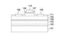
【解決手段】窒化物半導体装置は、サファイアからなる基板101上に順次形成され、それぞれ窒化物半導体からなる、バッファ層102と、下地層103と、第1の半導体層104と、第2の半導体層105と、コントロール層106と、コンタクト層107とを備えている。また、第2の半導体層105の上におけるコントロール層106の両測方の領域には、それぞれTi及びAlからなるソース電極108並びにドレイン電極109が形成され、コンタクト層107の上にはNiからなるゲート電極110が形成されている。
【選択図】図1
Description
M.Hikita et al., Technical Digest of 2004 International Electron Devices Meeting (2004) p.803 O. Ambacher et al., J.Appl.Phys. Vol.85 (1999) p.3222 L. Zhang et al., IEEE Transactions on Electron Devices, vol.47, no.3, pp.507-511, 2000
図1は本発明の第1の実施形態に係る窒化物半導体装置の断面構造の一例を示している。
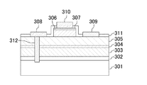
図3は本発明の第2の実施形態に係る窒化物半導体装置の断面構造の一例を示している。
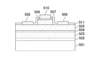
図5は本発明の第3の実施形態に係る窒化物半導体装置の断面構造の一例を示している。
102 バッファ層
103 下地層
104 第1の半導体層
105 第2の半導体層
106 コントロール層
107 コンタクト層
108 ソース電極
109 ドレイン電極
110 ゲート電極
111 パッシベーション膜
301 基板
302 バッファ層
303 下地層
304 第1の半導体層
305 第2の半導体層
306 コントロール層
307 コンタクト層
308 ソース電極
309 ドレイン電極
310 ゲート電極
311 パッシベーション膜
312 貫通穴
501 基板
502 バッファ層
503 下地層
504 第1の半導体層
505 第2の半導体層
506 コントロール層
507 コンタクト層
508 ソース電極
509 ドレイン電極
510 ゲート電極
511 パッシベーション膜
701 基板
702 アンドープGaN層
703 アンドープAl0.25Ga0.75N層
704 ソース電極
705 ドレイン電極
706 ゲート電極
707 パッシベーション膜
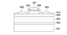
901 基板
902 AlNバッファ層
903 アンドープGaN層
904 アンドープAlGaN層
905 p型コントロール層
906 p型コンタクト層
907 ゲート電極
908 ソース電極
909 ドレイン電極
910 パッシベーション膜
Claims (6)
- 第1の窒化物半導体からなる第1の半導体層と、
前記第1の半導体層の主面上に形成され、バンドギャップが前記第1の窒化物半導体よりも大きい第2の窒化物半導体からなる第2の半導体層と、
前記第2の半導体層の上部又は上側に選択的に形成され、p型の導電性を有する第3の窒化物半導体からなるコントロール層と、
前記第2の半導体層の上で且つ前記コントロール層の両測方の領域にそれぞれ形成されたソース電極及びドレイン電極と、
前記コントロール層の上側に形成されたゲート電極と、
前記第1の半導体層の前記主面と反対側の面上に形成され、前記第1の窒化物半導体に対して価電子帯にポテンシャル障壁を有し、組成にアルミニウムを含む第4の窒化物半導体からなる第4の半導体層とを備えていることを特徴とする窒化物半導体装置。 - 前記コントロール層は、前記ゲート電極に順方向バイアスが印加された場合に、前記第1の半導体層に生じるチャネル領域にホールが注入され、前記ソース電極と前記ドレイン電極との間の電気伝導性を制御することを特徴とする請求項1に記載の窒化物半導体装置。
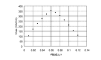
- 前記第4の半導体層におけるアルミニウムの組成比の値は、0.03以上且つ0.1以下に設定されていることを特徴とする請求項1又は2に記載の窒化物半導体装置。
- 前記第1の窒化物半導体は、組成にインジウムを含むことを特徴とする請求項1〜3のうちいずれか1項に記載の窒化物半導体装置。
- 前記第1の半導体層は、厚さが0nmより大きく且つ30nm以下であることを特徴とする請求項1〜4のうちいずれか1項に記載の窒化物半導体装置。
- 前記第1の窒化物半導体は、組成にインジウムを含み、
前記第1の半導体層は、厚さが0nmより大きく且つ30nm以下であることを特徴とする請求項3に記載の窒化物半導体装置。
Priority Applications (5)
| Application Number | Priority Date | Filing Date | Title |
|---|---|---|---|
| JP2006016622A JP4705481B2 (ja) | 2006-01-25 | 2006-01-25 | 窒化物半導体装置 |
| CNA2006101659295A CN101009324A (zh) | 2006-01-25 | 2006-12-11 | 氮化物半导体装置 |
| CN2011101620703A CN102244097A (zh) | 2006-01-25 | 2006-12-11 | 氮化物半导体装置 |
| US11/647,218 US7825434B2 (en) | 2006-01-25 | 2006-12-29 | Nitride semiconductor device |
| US12/879,565 US20100327320A1 (en) | 2006-01-25 | 2010-09-10 | Nitride semiconductor device |
Applications Claiming Priority (1)
| Application Number | Priority Date | Filing Date | Title |
|---|---|---|---|
| JP2006016622A JP4705481B2 (ja) | 2006-01-25 | 2006-01-25 | 窒化物半導体装置 |
Publications (2)
| Publication Number | Publication Date |
|---|---|
| JP2007201093A true JP2007201093A (ja) | 2007-08-09 |
| JP4705481B2 JP4705481B2 (ja) | 2011-06-22 |
Family
ID=38284671
Family Applications (1)
| Application Number | Title | Priority Date | Filing Date |
|---|---|---|---|
| JP2006016622A Expired - Lifetime JP4705481B2 (ja) | 2006-01-25 | 2006-01-25 | 窒化物半導体装置 |
Country Status (3)
| Country | Link |
|---|---|
| US (2) | US7825434B2 (ja) |
| JP (1) | JP4705481B2 (ja) |
| CN (2) | CN102244097A (ja) |
Cited By (4)
| Publication number | Priority date | Publication date | Assignee | Title |
|---|---|---|---|---|
| JP2010539712A (ja) * | 2007-09-12 | 2010-12-16 | トランスフォーム インコーポレイテッド | Iii族窒化物双方向スイッチ |
| JP2012019186A (ja) * | 2010-07-07 | 2012-01-26 | Samsung Electro-Mechanics Co Ltd | 窒化物系半導体素子及びその製造方法 |
| JP2014146744A (ja) * | 2013-01-30 | 2014-08-14 | Renesas Electronics Corp | 半導体装置 |
| WO2018181237A1 (ja) | 2017-03-31 | 2018-10-04 | パナソニックIpマネジメント株式会社 | 半導体装置 |
Families Citing this family (16)
| Publication number | Priority date | Publication date | Assignee | Title |
|---|---|---|---|---|
| US7531854B2 (en) | 2007-05-04 | 2009-05-12 | Dsm Solutions, Inc. | Semiconductor device having strain-inducing substrate and fabrication methods thereof |
| US7772056B2 (en) * | 2007-06-18 | 2010-08-10 | University Of Utah Research Foundation | Transistors for replacing metal-oxide semiconductor field-effect transistors in nanoelectronics |
| JP4478175B2 (ja) * | 2007-06-26 | 2010-06-09 | 株式会社東芝 | 半導体装置 |
| JP2009200395A (ja) * | 2008-02-25 | 2009-09-03 | Sanken Electric Co Ltd | Hfetおよびその製造方法 |
| JP2009231508A (ja) * | 2008-03-21 | 2009-10-08 | Panasonic Corp | 半導体装置 |
| EP2166085A1 (en) * | 2008-07-16 | 2010-03-24 | Suomen Punainen Risti Veripalvelu | Divalent modified cells |
| JP5595685B2 (ja) * | 2009-07-28 | 2014-09-24 | パナソニック株式会社 | 半導体装置 |
| US9378965B2 (en) * | 2009-12-10 | 2016-06-28 | Infineon Technologies Americas Corp. | Highly conductive source/drain contacts in III-nitride transistors |
| JP2011233751A (ja) * | 2010-04-28 | 2011-11-17 | Panasonic Corp | 窒化物半導体トランジスタ |
| JP5576731B2 (ja) * | 2010-07-14 | 2014-08-20 | パナソニック株式会社 | 電界効果トランジスタ |
| US8946788B2 (en) * | 2011-08-04 | 2015-02-03 | Avogy, Inc. | Method and system for doping control in gallium nitride based devices |
| CN102709321A (zh) | 2012-04-20 | 2012-10-03 | 程凯 | 增强型开关器件及其制造方法 |
| JP2014072427A (ja) * | 2012-09-28 | 2014-04-21 | Fujitsu Ltd | 半導体装置及び半導体装置の製造方法 |
| JP6189235B2 (ja) * | 2014-03-14 | 2017-08-30 | 株式会社東芝 | 半導体装置 |
| JP6642883B2 (ja) * | 2015-10-08 | 2020-02-12 | ローム株式会社 | 窒化物半導体装置およびその製造方法 |
| CN117855265A (zh) * | 2019-12-06 | 2024-04-09 | 联华电子股份有限公司 | 高电子迁移率晶体管及其制作方法 |
Citations (5)
| Publication number | Priority date | Publication date | Assignee | Title |
|---|---|---|---|---|
| JPS61230381A (ja) * | 1985-04-05 | 1986-10-14 | Nec Corp | 半導体装置 |
| JPH02177332A (ja) * | 1988-12-27 | 1990-07-10 | Nec Corp | 半導体装置 |
| JPH11261053A (ja) * | 1998-03-09 | 1999-09-24 | Furukawa Electric Co Ltd:The | 高移動度トランジスタ |
| JP2000299325A (ja) * | 1999-04-16 | 2000-10-24 | Hitachi Cable Ltd | 窒化ガリウム系化合物半導体を用いた電界効果トランジスタ用エピタキシャルウェハ |
| JP2001196575A (ja) * | 2000-01-13 | 2001-07-19 | Matsushita Electric Ind Co Ltd | 半導体装置 |
Family Cites Families (11)
| Publication number | Priority date | Publication date | Assignee | Title |
|---|---|---|---|---|
| DE3687049T2 (de) * | 1985-04-05 | 1993-03-25 | Nippon Electric Co | Bipolare eigenschaften aufweisender transistor mit heterouebergang. |
| JP3716906B2 (ja) * | 2000-03-06 | 2005-11-16 | 日本電気株式会社 | 電界効果トランジスタ |
| JP4906023B2 (ja) * | 2001-08-14 | 2012-03-28 | 古河電気工業株式会社 | GaN系半導体装置 |
| US7030428B2 (en) * | 2001-12-03 | 2006-04-18 | Cree, Inc. | Strain balanced nitride heterojunction transistors |
| JP3986887B2 (ja) * | 2002-05-17 | 2007-10-03 | 松下電器産業株式会社 | 半導体装置 |
| JP2004273486A (ja) | 2003-03-05 | 2004-09-30 | Mitsubishi Electric Corp | 半導体装置およびその製造方法 |
| US7098490B2 (en) * | 2003-06-02 | 2006-08-29 | Hrl Laboratories, Llc | GaN DHFET |
| US7382001B2 (en) * | 2004-01-23 | 2008-06-03 | International Rectifier Corporation | Enhancement mode III-nitride FET |
| JP4041075B2 (ja) * | 2004-02-27 | 2008-01-30 | 株式会社東芝 | 半導体装置 |
| JP4705412B2 (ja) | 2005-06-06 | 2011-06-22 | パナソニック株式会社 | 電界効果トランジスタ及びその製造方法 |
| JP4712459B2 (ja) | 2005-07-08 | 2011-06-29 | パナソニック株式会社 | トランジスタ及びその動作方法 |
-
2006
- 2006-01-25 JP JP2006016622A patent/JP4705481B2/ja not_active Expired - Lifetime
- 2006-12-11 CN CN2011101620703A patent/CN102244097A/zh active Pending
- 2006-12-11 CN CNA2006101659295A patent/CN101009324A/zh active Pending
- 2006-12-29 US US11/647,218 patent/US7825434B2/en active Active
-
2010
- 2010-09-10 US US12/879,565 patent/US20100327320A1/en not_active Abandoned
Patent Citations (5)
| Publication number | Priority date | Publication date | Assignee | Title |
|---|---|---|---|---|
| JPS61230381A (ja) * | 1985-04-05 | 1986-10-14 | Nec Corp | 半導体装置 |
| JPH02177332A (ja) * | 1988-12-27 | 1990-07-10 | Nec Corp | 半導体装置 |
| JPH11261053A (ja) * | 1998-03-09 | 1999-09-24 | Furukawa Electric Co Ltd:The | 高移動度トランジスタ |
| JP2000299325A (ja) * | 1999-04-16 | 2000-10-24 | Hitachi Cable Ltd | 窒化ガリウム系化合物半導体を用いた電界効果トランジスタ用エピタキシャルウェハ |
| JP2001196575A (ja) * | 2000-01-13 | 2001-07-19 | Matsushita Electric Ind Co Ltd | 半導体装置 |
Cited By (5)
| Publication number | Priority date | Publication date | Assignee | Title |
|---|---|---|---|---|
| JP2010539712A (ja) * | 2007-09-12 | 2010-12-16 | トランスフォーム インコーポレイテッド | Iii族窒化物双方向スイッチ |
| JP2012019186A (ja) * | 2010-07-07 | 2012-01-26 | Samsung Electro-Mechanics Co Ltd | 窒化物系半導体素子及びその製造方法 |
| JP2014146744A (ja) * | 2013-01-30 | 2014-08-14 | Renesas Electronics Corp | 半導体装置 |
| US9768257B2 (en) | 2013-01-30 | 2017-09-19 | Renesas Electronics Corporation | Semiconductor device |
| WO2018181237A1 (ja) | 2017-03-31 | 2018-10-04 | パナソニックIpマネジメント株式会社 | 半導体装置 |
Also Published As
| Publication number | Publication date |
|---|---|
| CN101009324A (zh) | 2007-08-01 |
| JP4705481B2 (ja) | 2011-06-22 |
| CN102244097A (zh) | 2011-11-16 |
| US20100327320A1 (en) | 2010-12-30 |
| US7825434B2 (en) | 2010-11-02 |
| US20070170463A1 (en) | 2007-07-26 |
Similar Documents
| Publication | Publication Date | Title |
|---|---|---|
| JP4712459B2 (ja) | トランジスタ及びその動作方法 | |
| JP5147197B2 (ja) | トランジスタ | |
| US8390029B2 (en) | Semiconductor device for reducing and/or preventing current collapse | |
| US8779438B2 (en) | Field-effect transistor with nitride semiconductor and method for fabricating the same | |
| JP6371986B2 (ja) | 窒化物半導体構造物 | |
| JP4705481B2 (ja) | 窒化物半導体装置 | |
| JP6229172B2 (ja) | 半導体装置 | |
| EP2747145B1 (en) | Field-effect transistor | |
| US20140110759A1 (en) | Semiconductor device | |
| JP2010135641A (ja) | 電界効果トランジスタ及びその製造方法 | |
| JP2008091392A (ja) | 窒化物半導体装置及びその製造方法 | |
| JP5691138B2 (ja) | 電界効果トランジスタ及びその製造方法 | |
| JP2011066464A (ja) | 電界効果トランジスタ | |
| JP5721782B2 (ja) | 半導体装置 | |
| JP2008130655A (ja) | 半導体素子 | |
| JP2011142358A (ja) | 窒化物半導体装置 | |
| JP2013239735A (ja) | 電界効果トランジスタ | |
| JP2015056413A (ja) | 窒化物半導体装置 |
Legal Events
| Date | Code | Title | Description |
|---|---|---|---|
| A621 | Written request for application examination |
Free format text: JAPANESE INTERMEDIATE CODE: A621 Effective date: 20080630 |
|
| A131 | Notification of reasons for refusal |
Free format text: JAPANESE INTERMEDIATE CODE: A131 Effective date: 20101116 |
|
| A521 | Request for written amendment filed |
Free format text: JAPANESE INTERMEDIATE CODE: A523 Effective date: 20101224 |
|
| TRDD | Decision of grant or rejection written | ||
| A01 | Written decision to grant a patent or to grant a registration (utility model) |
Free format text: JAPANESE INTERMEDIATE CODE: A01 Effective date: 20110215 |
|
| A61 | First payment of annual fees (during grant procedure) |
Free format text: JAPANESE INTERMEDIATE CODE: A61 Effective date: 20110311 |
|
| R150 | Certificate of patent or registration of utility model |
Ref document number: 4705481 Country of ref document: JP Free format text: JAPANESE INTERMEDIATE CODE: R150 |
|
| S533 | Written request for registration of change of name |
Free format text: JAPANESE INTERMEDIATE CODE: R313533 |
|
| R350 | Written notification of registration of transfer |
Free format text: JAPANESE INTERMEDIATE CODE: R350 |
|
| S111 | Request for change of ownership or part of ownership |
Free format text: JAPANESE INTERMEDIATE CODE: R313113 |
|
| R350 | Written notification of registration of transfer |
Free format text: JAPANESE INTERMEDIATE CODE: R350 |
|
| EXPY | Cancellation because of completion of term |