JP2007201704A - レベルシフト回路 - Google Patents
レベルシフト回路 Download PDFInfo
- Publication number
- JP2007201704A JP2007201704A JP2006016482A JP2006016482A JP2007201704A JP 2007201704 A JP2007201704 A JP 2007201704A JP 2006016482 A JP2006016482 A JP 2006016482A JP 2006016482 A JP2006016482 A JP 2006016482A JP 2007201704 A JP2007201704 A JP 2007201704A
- Authority
- JP
- Japan
- Prior art keywords
- level
- circuit
- differential pair
- current
- input signal
- Prior art date
- Legal status (The legal status is an assumption and is not a legal conclusion. Google has not performed a legal analysis and makes no representation as to the accuracy of the status listed.)
- Granted
Links
- 239000004065 semiconductor Substances 0.000 claims 1
- 101000988651 Homo sapiens Humanin-like 1 Proteins 0.000 description 21
- 238000010586 diagram Methods 0.000 description 15
- 101001081170 Homo sapiens Humanin-like 12 Proteins 0.000 description 9
- 102100027737 Humanin-like 12 Human genes 0.000 description 9
- 101001081172 Homo sapiens Humanin-like 11 Proteins 0.000 description 8
- 101000988650 Homo sapiens Humanin-like 13 Proteins 0.000 description 8
- 102100027736 Humanin-like 11 Human genes 0.000 description 8
- 102100029071 Humanin-like 13 Human genes 0.000 description 8
- 241001093403 Lettuce italian necrotic virus Species 0.000 description 6
- 238000005070 sampling Methods 0.000 description 6
- 230000015556 catabolic process Effects 0.000 description 5
- 230000008859 change Effects 0.000 description 3
- 238000006243 chemical reaction Methods 0.000 description 2
- 230000007246 mechanism Effects 0.000 description 2
- 230000008901 benefit Effects 0.000 description 1
- 238000004891 communication Methods 0.000 description 1
- 238000012937 correction Methods 0.000 description 1
- 238000006731 degradation reaction Methods 0.000 description 1
- 238000013461 design Methods 0.000 description 1
- 230000006866 deterioration Effects 0.000 description 1
- 238000007599 discharging Methods 0.000 description 1
- 238000000034 method Methods 0.000 description 1
- 238000012986 modification Methods 0.000 description 1
- 230000004048 modification Effects 0.000 description 1
- 238000012546 transfer Methods 0.000 description 1
- 230000001960 triggered effect Effects 0.000 description 1
Images





Landscapes
- Logic Circuits (AREA)
Abstract
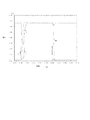
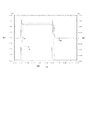
【解決手段】カレントミラー(HP1、HP2)を負荷とする差動対(HN1、HN2)は、入力信号INのローレベルおよびハイレベルにそれぞれ対応してローレベルおよびレベルシフトされたハイレベル(第2のハイレベル)となる出力信号OUTを非反転出力端子から出力する。非反転出力端子に接続されるプルアップ回路(HINV1、HP3)は、非反転出力信号が第2のハイレベルとなった場合に非反転出力端子をプルアップし、入力信号がローレベルである場合には開放となる。電流源制御回路(LNAND、HBUF)は、非反転出力信号が第2のハイレベルとなってから所定の時間経過後に差動対への動作電流を切断し、入力信号がローレベルになった時点で差動対への動作電流を供給するように、差動対と接地間に接続される電流源回路(LN1)を制御する。
【選択図】図1
Description
HINV1、HINV2、LINV インバータ回路
HN1、HN2、LN1 NMOSトランジスタ
HP1〜HP4、LP1 PMOSトランジスタ
LNAND NAND回路
VDDH 高電圧側電源
VDDL 低電圧側電源
Claims (6)
- カレントミラーを負荷とする差動対を含み、入力信号の第1のレベルおよび第2のレベルにそれぞれ対応して第1のレベルおよび第3のレベルとなる出力信号を非反転出力端子から出力するレベルシフト回路であって、
前記非反転出力端子に接続されると共に、前記非反転出力信号が第3のレベルとなった場合に前記非反転出力端子を前記差動対の電源と短絡し、前記入力信号が第1のレベルである場合には開放となる第1のプルアップ回路と、
前記差動対と接地間に接続されると共に、前記差動対への動作電流を供給する電流源回路と、
前記非反転出力信号が第3のレベルとなってから所定の時間経過後に前記差動対への動作電流を切断し、前記入力信号が第1のレベルである場合には前記差動対への動作電流を供給するように前記電流源回路を制御する電流源制御回路と、
を備えることを特徴とするレベルシフト回路。 - 前記差動対と前記第1のプルアップ回路には、高電源電圧が供給され、前記電流源回路と前記電流源制御回路には、低電源電圧が供給されることを特徴とする請求項1記載のレベルシフト回路。
- 前記電流源回路は、ドレインが前記差動対と接続され、ソースが接地され、ゲートが前記電流源制御回路の出力に接続される第1導電型のMOSトランジスタで構成されることを特徴とする請求項2記載のレベルシフト回路。
- 前記電流源回路は、ドレインが前記第1導電型のMOSトランジスタのドレインと接続され、ソースに前記低電源電圧が供給され、ゲートが前記第1導電型のMOSトランジスタのゲートに接続される第2導電型のMOSトランジスタをさらに含むことを特徴とする請求項3記載のレベルシフト回路。
- 前記差動対の反転出力端子に接続されると共に、該反転出力端子が第3のレベルとなった場合に前記反転出力端子を前記差動対の電源と短絡し、前記入力信号が第2のレベルである場合には開放となる第2のプルアップ回路をさらに備え、
前記第2のプルアップ回路には、前記高電源電圧が供給されることを特徴とする請求項2〜4のいずれか一に記載のレベルシフト回路。 - 請求項1〜5のいずれか一に記載のレベルシフト回路を含むことを特徴とする半導体集積回路装置。
Priority Applications (1)
| Application Number | Priority Date | Filing Date | Title |
|---|---|---|---|
| JP2006016482A JP4731333B2 (ja) | 2006-01-25 | 2006-01-25 | レベルシフト回路 |
Applications Claiming Priority (1)
| Application Number | Priority Date | Filing Date | Title |
|---|---|---|---|
| JP2006016482A JP4731333B2 (ja) | 2006-01-25 | 2006-01-25 | レベルシフト回路 |
Publications (2)
| Publication Number | Publication Date |
|---|---|
| JP2007201704A true JP2007201704A (ja) | 2007-08-09 |
| JP4731333B2 JP4731333B2 (ja) | 2011-07-20 |
Family
ID=38455850
Family Applications (1)
| Application Number | Title | Priority Date | Filing Date |
|---|---|---|---|
| JP2006016482A Expired - Fee Related JP4731333B2 (ja) | 2006-01-25 | 2006-01-25 | レベルシフト回路 |
Country Status (1)
| Country | Link |
|---|---|
| JP (1) | JP4731333B2 (ja) |
Cited By (8)
| Publication number | Priority date | Publication date | Assignee | Title |
|---|---|---|---|---|
| JP2009200563A (ja) * | 2008-02-19 | 2009-09-03 | Renesas Technology Corp | 電圧変換回路 |
| JP2009218735A (ja) * | 2008-03-07 | 2009-09-24 | Toshiba Corp | 半導体集積装置 |
| US7924080B2 (en) | 2009-02-10 | 2011-04-12 | Kabushiki Kaisha Toshiba | Level shifter circuit |
| KR20140121347A (ko) * | 2013-04-05 | 2014-10-15 | 가부시키가이샤 한도오따이 에네루기 켄큐쇼 | 신호 처리 장치 |
| US9660651B2 (en) | 2015-07-13 | 2017-05-23 | Denso Corporation | Level shift circuit |
| CN115425961A (zh) * | 2022-11-04 | 2022-12-02 | 西安水木芯邦半导体设计有限公司 | 一种高压模拟开关阵列电路 |
| CN117097324A (zh) * | 2023-09-04 | 2023-11-21 | 中科赛飞(广州)半导体有限公司 | 一种电平转移电路 |
| CN118018000A (zh) * | 2024-04-08 | 2024-05-10 | 瓴科微(上海)集成电路有限责任公司 | 一种防过冲的电平转换电路 |
Citations (6)
| Publication number | Priority date | Publication date | Assignee | Title |
|---|---|---|---|---|
| JPH04160815A (ja) * | 1990-10-25 | 1992-06-04 | Toshiba Corp | 出力バッファ回路 |
| JPH07226670A (ja) * | 1994-02-14 | 1995-08-22 | Matsushita Electric Ind Co Ltd | Cmosレベルシフト回路 |
| JPH098570A (ja) * | 1995-06-15 | 1997-01-10 | New Japan Radio Co Ltd | Cmos演算増幅器 |
| JPH11214979A (ja) * | 1998-01-28 | 1999-08-06 | Hitachi Ltd | 半導体集積回路 |
| JP2003298408A (ja) * | 2002-04-02 | 2003-10-17 | New Japan Radio Co Ltd | レベル変換回路 |
| JP2006121654A (ja) * | 2004-09-21 | 2006-05-11 | Renesas Technology Corp | レベル変換回路 |
-
2006
- 2006-01-25 JP JP2006016482A patent/JP4731333B2/ja not_active Expired - Fee Related
Patent Citations (6)
| Publication number | Priority date | Publication date | Assignee | Title |
|---|---|---|---|---|
| JPH04160815A (ja) * | 1990-10-25 | 1992-06-04 | Toshiba Corp | 出力バッファ回路 |
| JPH07226670A (ja) * | 1994-02-14 | 1995-08-22 | Matsushita Electric Ind Co Ltd | Cmosレベルシフト回路 |
| JPH098570A (ja) * | 1995-06-15 | 1997-01-10 | New Japan Radio Co Ltd | Cmos演算増幅器 |
| JPH11214979A (ja) * | 1998-01-28 | 1999-08-06 | Hitachi Ltd | 半導体集積回路 |
| JP2003298408A (ja) * | 2002-04-02 | 2003-10-17 | New Japan Radio Co Ltd | レベル変換回路 |
| JP2006121654A (ja) * | 2004-09-21 | 2006-05-11 | Renesas Technology Corp | レベル変換回路 |
Cited By (12)
| Publication number | Priority date | Publication date | Assignee | Title |
|---|---|---|---|---|
| JP2009200563A (ja) * | 2008-02-19 | 2009-09-03 | Renesas Technology Corp | 電圧変換回路 |
| JP2009218735A (ja) * | 2008-03-07 | 2009-09-24 | Toshiba Corp | 半導体集積装置 |
| US7839198B2 (en) | 2008-03-07 | 2010-11-23 | Kabushiki Kaisha Toshiba | Semiconductor integrated device |
| US7924080B2 (en) | 2009-02-10 | 2011-04-12 | Kabushiki Kaisha Toshiba | Level shifter circuit |
| KR20140121347A (ko) * | 2013-04-05 | 2014-10-15 | 가부시키가이샤 한도오따이 에네루기 켄큐쇼 | 신호 처리 장치 |
| JP2014225867A (ja) * | 2013-04-05 | 2014-12-04 | 株式会社半導体エネルギー研究所 | 信号処理装置 |
| KR102127994B1 (ko) * | 2013-04-05 | 2020-06-29 | 가부시키가이샤 한도오따이 에네루기 켄큐쇼 | 신호 처리 장치 |
| US9660651B2 (en) | 2015-07-13 | 2017-05-23 | Denso Corporation | Level shift circuit |
| CN115425961A (zh) * | 2022-11-04 | 2022-12-02 | 西安水木芯邦半导体设计有限公司 | 一种高压模拟开关阵列电路 |
| CN117097324A (zh) * | 2023-09-04 | 2023-11-21 | 中科赛飞(广州)半导体有限公司 | 一种电平转移电路 |
| CN117097324B (zh) * | 2023-09-04 | 2024-05-31 | 中科赛飞(广州)半导体有限公司 | 一种电平转移电路 |
| CN118018000A (zh) * | 2024-04-08 | 2024-05-10 | 瓴科微(上海)集成电路有限责任公司 | 一种防过冲的电平转换电路 |
Also Published As
| Publication number | Publication date |
|---|---|
| JP4731333B2 (ja) | 2011-07-20 |
Similar Documents
| Publication | Publication Date | Title |
|---|---|---|
| KR100472836B1 (ko) | 고속 샘플링 수신기 | |
| CN101873129B (zh) | 使用交叉耦合级联晶体管的电平移位 | |
| CN113162601B (zh) | 具有电压容忍力的电平移位器 | |
| TWI792232B (zh) | 工作週期校正電路及其方法 | |
| KR100829779B1 (ko) | 레벨 쉬프팅 회로 | |
| US10418998B1 (en) | Level shifter circuit and method thereof | |
| JP4731333B2 (ja) | レベルシフト回路 | |
| JPH04229719A (ja) | プルアップ抵抗コントロール入力回路及び出力回路 | |
| US8653879B2 (en) | Level shifter and semiconductor integrated circuit including the shifter | |
| US9071240B2 (en) | Low power, single-rail level shifters employing power down signal from output power domain and a method of converting a data signal between power domains | |
| CN101931374A (zh) | 差分信号接收电路和显示设备 | |
| US9191006B1 (en) | Current-limited level shift circuit | |
| JP2004228879A (ja) | レベルシフト回路 | |
| JP4386918B2 (ja) | レベルシフト回路及びこれを備えた半導体集積回路 | |
| CN111682873A (zh) | 一种低功耗输出缓冲器电路 | |
| JP4774287B2 (ja) | 出力回路 | |
| JP2007180797A (ja) | レベルシフト回路 | |
| JP4724575B2 (ja) | レベル変換回路 | |
| US20090160517A1 (en) | Flip-flop | |
| KR102676329B1 (ko) | 레벨 쉬프터 및 이를 포함하는 반도체 장치 | |
| TWI893731B (zh) | 電源水平檢測電路及兩級電源域電路 | |
| JP2003152528A (ja) | Cmosバッファ回路 | |
| TWM586017U (zh) | 低功率電位轉換器 | |
| JP2012169810A (ja) | レベルシフト回路 | |
| JP4667190B2 (ja) | レベル変換回路 |
Legal Events
| Date | Code | Title | Description |
|---|---|---|---|
| A621 | Written request for application examination |
Free format text: JAPANESE INTERMEDIATE CODE: A621 Effective date: 20081212 |
|
| A977 | Report on retrieval |
Free format text: JAPANESE INTERMEDIATE CODE: A971007 Effective date: 20110223 |
|
| TRDD | Decision of grant or rejection written | ||
| A01 | Written decision to grant a patent or to grant a registration (utility model) |
Free format text: JAPANESE INTERMEDIATE CODE: A01 Effective date: 20110419 |
|
| A01 | Written decision to grant a patent or to grant a registration (utility model) |
Free format text: JAPANESE INTERMEDIATE CODE: A01 |
|
| A61 | First payment of annual fees (during grant procedure) |
Free format text: JAPANESE INTERMEDIATE CODE: A61 Effective date: 20110419 |
|
| FPAY | Renewal fee payment (event date is renewal date of database) |
Free format text: PAYMENT UNTIL: 20140428 Year of fee payment: 3 |
|
| R150 | Certificate of patent or registration of utility model |
Free format text: JAPANESE INTERMEDIATE CODE: R150 |
|
| LAPS | Cancellation because of no payment of annual fees |