JP2007227984A - 基板処理装置 - Google Patents
基板処理装置 Download PDFInfo
- Publication number
- JP2007227984A JP2007227984A JP2007157723A JP2007157723A JP2007227984A JP 2007227984 A JP2007227984 A JP 2007227984A JP 2007157723 A JP2007157723 A JP 2007157723A JP 2007157723 A JP2007157723 A JP 2007157723A JP 2007227984 A JP2007227984 A JP 2007227984A
- Authority
- JP
- Japan
- Prior art keywords
- substrate
- processing
- units
- unit
- process module
- Prior art date
- Legal status (The legal status is an assumption and is not a legal conclusion. Google has not performed a legal analysis and makes no representation as to the accuracy of the status listed.)
- Pending
Links
Images



Landscapes
- Exposure Of Semiconductors, Excluding Electron Or Ion Beam Exposure (AREA)
Abstract
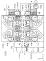
【解決手段】処理ユニットを配置した複数の処理経路を、往復することよって一連の処理が可能となるように、積層配置する。これにより平面占有面積の低減と基板処理能力の増大が図れる。また、役割および動作範囲が限定された移載ロボットR1、R3〜R10を同時かつ並行に動作させることにより、各処理ユニットにおいて間断なき処理が可能となり、処理効率を高めることができる。
【選択図】図2
Description
図1は、本発明の実施の形態に係る基板処理装置1の構成の概要を示す図である。図1に示すように、基板処理装置1は、装置外部との間で基板の授受を担うインデクサIDと、基板に対し所定の処理を施す複数の処理ユニットからなるプロセスモジュールPMと、露光装置であるステッパSTPとの間で基板を受け渡すインタフェースIFとを備える。なお、図1にはxyz3次元座標系を付しており、xyが水平面方向、zが鉛直方向を指し示している。以降の説明において、座標系は原則としてこれに従うものとする。
図2は、基板処理装置1の下段部LFの構成を示す図、図3は基板処理装置1の上段部UFの構成を示す図である。以下、図2および図3に基づいて、基板処理装置各部の構成を説明する。
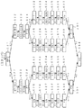
以下、上述のような構成をとる基板処理装置1において、どのような処理シーケンスにて基板Wにおける回路パターンの形成がなされるのか、および、その際に基板がどのように搬送されていくのかを説明する。図4は、基板処理装置1の下段部LFにおいてなされる、一連の処理についてのフローを示す図である。図5は、基板処理装置1の上段部UFにおいてなされる、一連の処理についてのフローを示す図である。なお、図4および図5においては、各処理ユニット間で移載を担う移載ロボットの符号を、矢印の近傍に付している。
上段部UFと下段部LFの機能は、入れ替わってもよい。すなわち、上段部UFにてレジスト塗布処理等がなされ、下段部LFにて現像処理がなされる構成であってもよい。あるいは、処理経路をさらに備え、これらが多段に配置されていてもよい。
11〜22 多段熱処理部
31、32 エッジ露光部
33、34 多段露光後熱処理部
41 メンテナンスエリア
A1〜A4 疎水化処理ユニット
AM1〜AM22 アーム
B1〜B6 露光後ベークユニット
BARC1〜BARC4 反射防止膜塗布処理ユニット
BF1、BF2 バッファカセット
C カセット
C1〜C16、C21〜C26 冷却処理ユニット
E1〜E4 エッジ露光ユニット
H1〜H22 加熱処理ユニット
ID インデクサ
IF インタフェース
P1〜P12 パスユニット
PM プロセスモジュール
R1〜R22 移載ロボット
S1〜S38 ステップ
SC1〜SC4 レジスト塗布処理ユニット
SD1〜SD8 現像処理ユニット
W 基板
Claims (1)
- 基板処理装置であって、
それぞれが複数の処理ユニットを含むユニット群を有し、所定の基板処理シーケンスに係る処理を行う複数のプロセス部が積層配置されてなり、
前記複数のプロセス部が少なくとも、前記基板処理シーケンスとして薬液膜の形成を行う第1のプロセス部と基板に形成された露光パターンの現像を行う第2のプロセス部とを有してなり、
前記複数のプロセス部がいずれも、
それぞれにおいて前記ユニット群に含まれる少なくとも1つのユニットが配置された複数のユニット配置部と、
前記複数のユニット配置部の間に設けられ、基板の受け渡しを行う受け渡し手段と、
前記プロセス部において処理待ち状態の基板を収容可能な収容手段と、
を備えることを特徴とする基板処理装置。
Priority Applications (1)
| Application Number | Priority Date | Filing Date | Title |
|---|---|---|---|
| JP2007157723A JP2007227984A (ja) | 2007-06-14 | 2007-06-14 | 基板処理装置 |
Applications Claiming Priority (1)
| Application Number | Priority Date | Filing Date | Title |
|---|---|---|---|
| JP2007157723A JP2007227984A (ja) | 2007-06-14 | 2007-06-14 | 基板処理装置 |
Related Parent Applications (1)
| Application Number | Title | Priority Date | Filing Date |
|---|---|---|---|
| JP2002169556A Division JP2004014966A (ja) | 2002-06-11 | 2002-06-11 | 基板処理装置 |
Publications (1)
| Publication Number | Publication Date |
|---|---|
| JP2007227984A true JP2007227984A (ja) | 2007-09-06 |
Family
ID=38549397
Family Applications (1)
| Application Number | Title | Priority Date | Filing Date |
|---|---|---|---|
| JP2007157723A Pending JP2007227984A (ja) | 2007-06-14 | 2007-06-14 | 基板処理装置 |
Country Status (1)
| Country | Link |
|---|---|
| JP (1) | JP2007227984A (ja) |
Cited By (5)
| Publication number | Priority date | Publication date | Assignee | Title |
|---|---|---|---|---|
| US8545118B2 (en) | 2007-11-30 | 2013-10-01 | Sokudo Co., Ltd. | Substrate treating apparatus with inter-unit buffers |
| US9165807B2 (en) | 2007-06-29 | 2015-10-20 | Screen Semiconductor Solutions Co., Ltd. | Substrate treating apparatus with vertical treatment arrangement including vertical blowout and exhaust units |
| US9184071B2 (en) | 2007-11-30 | 2015-11-10 | Screen Semiconductor Solutions Co., Ltd. | Multi-story substrate treating apparatus with flexible transport mechanisms and vertically divided treating units |
| US9299596B2 (en) | 2007-12-28 | 2016-03-29 | Screen Semiconductor Solutions Co., Ltd. | Substrate treating apparatus with parallel substrate treatment lines simultaneously treating a plurality of substrates |
| US9368383B2 (en) | 2007-12-28 | 2016-06-14 | Screen Semiconductor Solutions Co., Ltd. | Substrate treating apparatus with substrate reordering |
Citations (10)
| Publication number | Priority date | Publication date | Assignee | Title |
|---|---|---|---|---|
| JPH0846010A (ja) * | 1994-08-04 | 1996-02-16 | Tokyo Electron Ltd | 処理システム |
| JPH1187456A (ja) * | 1997-09-12 | 1999-03-30 | Dainippon Screen Mfg Co Ltd | 基板処理装置 |
| JPH11251399A (ja) * | 1998-02-27 | 1999-09-17 | Dainippon Screen Mfg Co Ltd | 基板処理装置 |
| JP2000124129A (ja) * | 1998-08-14 | 2000-04-28 | Tokyo Electron Ltd | 処理装置 |
| JP2001077176A (ja) * | 1999-07-02 | 2001-03-23 | Tokyo Electron Ltd | 基板処理装置 |
| JP2001093827A (ja) * | 1999-07-16 | 2001-04-06 | Tokyo Electron Ltd | 処理システム |
| JP2001093828A (ja) * | 2000-07-14 | 2001-04-06 | Tokyo Electron Ltd | 処理システム |
| JP2001168004A (ja) * | 1999-12-08 | 2001-06-22 | Tokyo Electron Ltd | 基板処理装置 |
| JP2001176792A (ja) * | 1999-12-06 | 2001-06-29 | Dns Korea Co Ltd | 半導体製造のためのフォトリソグラフィ装置 |
| JP2001189369A (ja) * | 1999-10-19 | 2001-07-10 | Tokyo Electron Ltd | 基板処理装置 |
-
2007
- 2007-06-14 JP JP2007157723A patent/JP2007227984A/ja active Pending
Patent Citations (10)
| Publication number | Priority date | Publication date | Assignee | Title |
|---|---|---|---|---|
| JPH0846010A (ja) * | 1994-08-04 | 1996-02-16 | Tokyo Electron Ltd | 処理システム |
| JPH1187456A (ja) * | 1997-09-12 | 1999-03-30 | Dainippon Screen Mfg Co Ltd | 基板処理装置 |
| JPH11251399A (ja) * | 1998-02-27 | 1999-09-17 | Dainippon Screen Mfg Co Ltd | 基板処理装置 |
| JP2000124129A (ja) * | 1998-08-14 | 2000-04-28 | Tokyo Electron Ltd | 処理装置 |
| JP2001077176A (ja) * | 1999-07-02 | 2001-03-23 | Tokyo Electron Ltd | 基板処理装置 |
| JP2001093827A (ja) * | 1999-07-16 | 2001-04-06 | Tokyo Electron Ltd | 処理システム |
| JP2001189369A (ja) * | 1999-10-19 | 2001-07-10 | Tokyo Electron Ltd | 基板処理装置 |
| JP2001176792A (ja) * | 1999-12-06 | 2001-06-29 | Dns Korea Co Ltd | 半導体製造のためのフォトリソグラフィ装置 |
| JP2001168004A (ja) * | 1999-12-08 | 2001-06-22 | Tokyo Electron Ltd | 基板処理装置 |
| JP2001093828A (ja) * | 2000-07-14 | 2001-04-06 | Tokyo Electron Ltd | 処理システム |
Cited By (11)
| Publication number | Priority date | Publication date | Assignee | Title |
|---|---|---|---|---|
| US9165807B2 (en) | 2007-06-29 | 2015-10-20 | Screen Semiconductor Solutions Co., Ltd. | Substrate treating apparatus with vertical treatment arrangement including vertical blowout and exhaust units |
| US9174235B2 (en) | 2007-06-29 | 2015-11-03 | Screen Semiconductor Solutions Co., Ltd. | Substrate treating apparatus using horizontal treatment cell arrangements with parallel treatment lines |
| US9230834B2 (en) | 2007-06-29 | 2016-01-05 | Screen Semiconductor Solutions Co., Ltd. | Substrate treating apparatus |
| US10290521B2 (en) | 2007-06-29 | 2019-05-14 | Screen Semiconductor Solutions Co., Ltd. | Substrate treating apparatus with parallel gas supply pipes and a gas exhaust pipe |
| US8545118B2 (en) | 2007-11-30 | 2013-10-01 | Sokudo Co., Ltd. | Substrate treating apparatus with inter-unit buffers |
| US8708587B2 (en) | 2007-11-30 | 2014-04-29 | Sokudo Co., Ltd. | Substrate treating apparatus with inter-unit buffers |
| US9184071B2 (en) | 2007-11-30 | 2015-11-10 | Screen Semiconductor Solutions Co., Ltd. | Multi-story substrate treating apparatus with flexible transport mechanisms and vertically divided treating units |
| US9687874B2 (en) | 2007-11-30 | 2017-06-27 | Screen Semiconductor Solutions Co., Ltd. | Multi-story substrate treating apparatus with flexible transport mechanisms and vertically divided treating units |
| US9299596B2 (en) | 2007-12-28 | 2016-03-29 | Screen Semiconductor Solutions Co., Ltd. | Substrate treating apparatus with parallel substrate treatment lines simultaneously treating a plurality of substrates |
| US9368383B2 (en) | 2007-12-28 | 2016-06-14 | Screen Semiconductor Solutions Co., Ltd. | Substrate treating apparatus with substrate reordering |
| US12217986B2 (en) | 2007-12-28 | 2025-02-04 | Screen Semiconductor Solutions Co., Ltd. | Substrate treating apparatus with parallel first and second parts of substrate treatment lines on multiple stories for simultaneously treating a plurality of substrates |
Similar Documents
| Publication | Publication Date | Title |
|---|---|---|
| US7980003B2 (en) | Heat processing apparatus and heat processing method | |
| JP5267720B2 (ja) | 塗布、現像装置、塗布、現像方法及び記憶媒体 | |
| US8023099B2 (en) | Substrate processing system and substrate processing method for double patterning with carrier block, process section, and interface block | |
| US8236132B2 (en) | Substrate processing system and substrate transfer method | |
| JP2004260129A (ja) | 基板処理装置および基板処理装置における基板搬送方法および基板処理方法 | |
| JPH1092733A (ja) | 処理システム | |
| US20100192844A1 (en) | Apparatus and method for treating substrate | |
| JP2002217267A (ja) | 基板処理装置 | |
| JP4687682B2 (ja) | 塗布、現像装置及びその方法並びに記憶媒体 | |
| JP4401879B2 (ja) | 基板の回収方法及び基板処理装置 | |
| US9566598B2 (en) | Substrate processing apparatus and substrate processing method | |
| JPH1079343A (ja) | 処理方法及び塗布現像処理システム | |
| JP2007227984A (ja) | 基板処理装置 | |
| US7575382B2 (en) | Coating/developing apparatus and operation method thereof | |
| US20100204821A1 (en) | Substrate treatment apparatus | |
| JP4080405B2 (ja) | 基板処理装置 | |
| TW201526136A (zh) | 基板處理裝置、基板處理方法、暨基板處理系統 | |
| KR20140116782A (ko) | 기판 처리 장치 | |
| JP2004014966A (ja) | 基板処理装置 | |
| US7678417B2 (en) | Coating method and coating apparatus | |
| KR101018525B1 (ko) | 기판 처리 장치 및 기판 처리 방법 | |
| JP2010192559A (ja) | 基板処理システム | |
| JP4262037B2 (ja) | 基板処理装置 | |
| JP7114424B2 (ja) | 基板処理装置および基板処理方法 | |
| JP4606159B2 (ja) | 基板処理装置、基板処理方法、コンピュータプログラム及び記憶媒体 |
Legal Events
| Date | Code | Title | Description |
|---|---|---|---|
| A621 | Written request for application examination |
Free format text: JAPANESE INTERMEDIATE CODE: A621 Effective date: 20070615 |
|
| RD04 | Notification of resignation of power of attorney |
Free format text: JAPANESE INTERMEDIATE CODE: A7424 Effective date: 20091217 |
|
| A131 | Notification of reasons for refusal |
Free format text: JAPANESE INTERMEDIATE CODE: A131 Effective date: 20100622 |
|
| A521 | Request for written amendment filed |
Free format text: JAPANESE INTERMEDIATE CODE: A523 Effective date: 20100817 |
|
| A131 | Notification of reasons for refusal |
Free format text: JAPANESE INTERMEDIATE CODE: A131 Effective date: 20101012 |
|
| A521 | Request for written amendment filed |
Free format text: JAPANESE INTERMEDIATE CODE: A523 Effective date: 20101210 |
|
| A02 | Decision of refusal |
Free format text: JAPANESE INTERMEDIATE CODE: A02 Effective date: 20110125 |