JP2007258332A - Photoelectric conversion element, photoelectric conversion element manufacturing method, imaging apparatus, imaging apparatus manufacturing method, and radiation imaging apparatus - Google Patents
Photoelectric conversion element, photoelectric conversion element manufacturing method, imaging apparatus, imaging apparatus manufacturing method, and radiation imaging apparatus Download PDFInfo
- Publication number
- JP2007258332A JP2007258332A JP2006078578A JP2006078578A JP2007258332A JP 2007258332 A JP2007258332 A JP 2007258332A JP 2006078578 A JP2006078578 A JP 2006078578A JP 2006078578 A JP2006078578 A JP 2006078578A JP 2007258332 A JP2007258332 A JP 2007258332A
- Authority
- JP
- Japan
- Prior art keywords
- type semiconductor
- photoelectric conversion
- electrode
- conversion element
- dopant
- Prior art date
- Legal status (The legal status is an assumption and is not a legal conclusion. Google has not performed a legal analysis and makes no representation as to the accuracy of the status listed.)
- Pending
Links
Images




Landscapes
- Transforming Light Signals Into Electric Signals (AREA)
- Light Receiving Elements (AREA)
- Electroluminescent Light Sources (AREA)
- Solid State Image Pick-Up Elements (AREA)
Abstract
【課題】暗電流を少なくすることで画質が良く、生産効率の良い光電変換素子、この光電変換素子を用いた撮像装置及び放射線撮像装置を提供する。
【解決手段】I型半導体の両側が電極で挟まれて成る光電変換素子において、前記電極の一方が前記I型半導体をN型半導体にするドーパントを含み、該ドーパントの移行により形成されるN型半導体層を有する構成、及び、前記電極の他方が前記I型半導体をP型半導体にするドーパントを含み、該ドーパントの移行により形成されるP型半導体層を有する構成、の少なくとも一方の構成を有する。
【選択図】図1
The present invention provides a photoelectric conversion element with high image quality and low production efficiency by reducing dark current, and an imaging apparatus and a radiation imaging apparatus using the photoelectric conversion element.
In a photoelectric conversion element in which both sides of an I-type semiconductor are sandwiched between electrodes, one of the electrodes includes a dopant that makes the I-type semiconductor an N-type semiconductor, and an N-type formed by migration of the dopant At least one of a configuration having a semiconductor layer and a configuration in which the other of the electrodes includes a dopant that makes the I-type semiconductor a P-type semiconductor and has a P-type semiconductor layer formed by migration of the dopant. .
[Selection] Figure 1
Description
本発明は、光電変換素子、光電変換素子の製造方法、撮像装置、撮像装置の製造方法及び放射線撮像装置及び放射線撮像装置に関する。 The present invention relates to a photoelectric conversion element, a photoelectric conversion element manufacturing method, an imaging apparatus, an imaging apparatus manufacturing method, a radiation imaging apparatus, and a radiation imaging apparatus.
近年、画像を電気信号として取得する方法として、CCDイメージセンサやCMOSイメージセンサが広く使われている。これらの多くは、シリコン等の結晶基板上に製造されているため、撮像エリアは、結晶基板のサイズで制限されることになる。 In recent years, CCD image sensors and CMOS image sensors have been widely used as methods for acquiring images as electrical signals. Since many of these are manufactured on a crystal substrate such as silicon, the imaging area is limited by the size of the crystal substrate.
一方、例えば、光源にX線を使用する医療・検査関連分野において、大面積の撮像エリアを有するイメージセンサに対する需要が高まってきている。例えば、医療業界において、人体の胸部のX線画像を放射線写真フィルムを介さず直接電気信号として得る手段として、放射線を蛍光体によって放射線の強度に比例した可視光に変換し、それを光電変換素子を用いて電気信号に変換することの出来る半導体センサを用い、変換された電気信号を、薄膜トランジスタを用いた回路で読み出すフラットパネルディテクタ(以下、FPDと称する。)と呼ばれる放射線撮像装置がある。こうした大面積の撮像装置は、半導体膜をガラス等の基板上に堆積させるなどの方法で製造される。 On the other hand, for example, in a medical / inspection related field using X-rays as a light source, there is an increasing demand for an image sensor having a large imaging area. For example, in the medical industry, as a means for obtaining an X-ray image of a human breast directly as an electrical signal without going through a radiographic film, the radiation is converted into visible light proportional to the intensity of the radiation by a phosphor, and the photoelectric conversion element There is a radiation imaging apparatus called a flat panel detector (hereinafter referred to as FPD) that uses a semiconductor sensor that can be converted into an electric signal by using a circuit and reads out the converted electric signal by a circuit using a thin film transistor. Such a large-area imaging device is manufactured by a method of depositing a semiconductor film on a substrate such as glass.
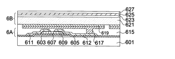
ガラス基板の上に形成された半導体膜を有するPIN型光電変換素子及び薄膜トランジスタを含む画素を複数有するイメージセンサの1画素の断面構造の例を模式的に図6及び図7に示す。 An example of a cross-sectional structure of one pixel of an image sensor including a plurality of pixels including a PIN photoelectric conversion element having a semiconductor film formed on a glass substrate and a thin film transistor is shown in FIGS.
図6において、601はガラス基板、603はゲート電極、605はゲート絶縁膜を含む絶縁層、607は半導体層、609はオーミックコンタクト層、611はソース電極、612はドレイン電極、617画素電極、619はN型半導体層、621はI型半導体層、623はP型半導体層、625は共通電極、615及び627はパッシベーション膜である。また、図7において、701はガラス基板、703はゲート電極、705はゲート絶縁膜を含む絶縁層、707は半導体層、709はオーミックコンタクト層、711はソース電極、712はドレイン電極、715は接続電極、717画素電極、719はN型半導体層、721はI型半導体層、723はP型半導体層、725は共通電極、727及び729はパッシベーション膜である。 In FIG. 6, 601 is a glass substrate, 603 is a gate electrode, 605 is an insulating layer including a gate insulating film, 607 is a semiconductor layer, 609 is an ohmic contact layer, 611 is a source electrode, 612 is a drain electrode, 617 pixel electrode, 619 Is an N-type semiconductor layer, 621 is an I-type semiconductor layer, 623 is a P-type semiconductor layer, 625 is a common electrode, and 615 and 627 are passivation films. In FIG. 7, 701 is a glass substrate, 703 is a gate electrode, 705 is an insulating layer including a gate insulating film, 707 is a semiconductor layer, 709 is an ohmic contact layer, 711 is a source electrode, 712 is a drain electrode, and 715 is a connection. An electrode, 717 pixel electrode, 719 is an N-type semiconductor layer, 721 is an I-type semiconductor layer, 723 is a P-type semiconductor layer, 725 is a common electrode, and 727 and 729 are passivation films.
図6及び図7にそれぞれ示す画素は、光を電荷に変換するためのPIN型光電変換素子6B及び7Bと、電荷による電気信号を読み出すためのスイッチング素子である薄膜トランジスタ6A及び7Aとで構成される。この画素を2次元マトリクス状に配置することで撮像装置を構成することができ、また、図6及び図7の上部、例えば、図6のパッシベーション膜627の上に、放射線であるX線を光に変えるシンチレーターを設けることで、上述のFPDを構成することが出来る。
Each pixel shown in FIGS. 6 and 7 is composed of PIN
上述の光電変換素子6B及び7Bは、画素毎に電気的に十分に分離されていることが要望されている。光電変換素子6B及び7Bが電気的に分離されることで画素毎に入る光による電荷のみを薄膜トランジスタを通じて撮層装置の外に出力することができるため、撮層装置を構成する画素数に見合った十分な解像力が確保される。
The above-described
光電変換素子6B及び7Bを画素毎に電気的に分離する方法として、図6に示すような、ガラス基板601の上に形成された薄膜トランジスタ6Aで構成される読み出し回路の上に光電変換素子6Bが積層されてなる画素の場合、光電変換素子6Bを構成する少なくとも画素電極617側の抵抗の低いN型半導体層619を独立した状態とすることで画素毎の電気的な分離を実現している。
As a method of electrically separating the
また、図7に示すガラス基板701の同じ面上に薄膜トランジスタ7Aで構成される読み出し回路と光電変換素子7Bとでなる画素の場合、光電変換素子7Bを積層された光電変換膜をエッチングして物理的に分離した状態に形成することで画素毎の電気的な分離を実現している。
In the case of a pixel including a readout circuit composed of a
また、光電変換素子の感度は高いことが要望されている。これは、上述のFPDを例にすれば、X線の人体への暴射量を少なくすることで人体へ影響を抑えることが可能となり、また解像度と相まって画質をよくすることで診断に十分な情報を提供出来ることになるからである。こうした高い感度の要望に応えるためには、光電変換素子から発生するノイズを低減することが必要である。 Moreover, it is desired that the photoelectric conversion element has high sensitivity. Taking the above FPD as an example, it is possible to suppress the influence on the human body by reducing the amount of X-rays exposed to the human body, and it is sufficient for diagnosis by improving the image quality in combination with the resolution. This is because information can be provided. In order to meet such a demand for high sensitivity, it is necessary to reduce noise generated from the photoelectric conversion element.
図6に示すような薄膜トランジスタで構成される読み出し回路の上に光電変換素子が積層された画素を有する放射線撮像装置の例として、以下がある。放射線を光に変換する波長変換手段と、放射線を電荷に変換すると共に波長変換手段からの光を電荷に変換する電荷変換手段と、電荷変換手段で変換された電荷を蓄積する蓄積手段と、蓄積手段に蓄積された電荷に基づく信号を読み出す読出手段と、読出手段で読み出された電荷を出力する出力線とを備えた構成をし、電荷変換手段を、少なくとも絶縁性基板に形成すると共に、電荷蓄積手段、読出手段、出力線を、絶縁性基板の一面に形成し、波長変換手段を、電荷変換手段に積層すると共に、電荷変換手段を、絶縁性基板における電荷蓄積手段、読出手段、出力線の形成面に積層し、電荷変換手段と絶縁性基板上の電荷蓄積容量を、接続電極を介して電気的に接続してある(特許文献1参照)。
FPD等の撮像装置が有する画素を構成する光電変換素子をエッチングや膜形成を伴って半導体層を形成することで製造する場合、エッチングされた表面及び薄膜形成において不連続となる境界は、格子が不連続となることから生じる欠陥や不純物の混入が生じ易い。こうした欠陥や不純物の混入は、ノイズとなる暗電流が増加する要因となる。 When manufacturing a photoelectric conversion element constituting a pixel included in an imaging device such as an FPD by forming a semiconductor layer with etching or film formation, the boundary between the etched surface and the thin film formation is discontinuous by a lattice. Defects and impurities are likely to occur due to discontinuity. Such inclusion of defects and impurities causes an increase in noise dark current.
例えば、図6に示すPIN型光電変換素子6Bの作製おいては、作製途中に一旦真空成膜装置から取り出し、フォトリソグラフィー処理とエッチング処理によりN型半導体層619のパターニングを実施する必要がある。このパターニング工程により、PIN型光電変換素子6Bを構成する半導体層の成膜が不連続となる界面が生じ、この界面で欠陥や不純物の混入が生じる。このような欠陥や不純物の混入により画像の電気信号に重畳するノイズとなる暗電流が増加する。
For example, in the production of the PIN
一方、図7に示すPIN型光電変換素子7BはP型半導体層723、I型半導体層275及びN型半導体層719と連続成膜することが可能であるが、PIN型光電変換素子7Bを物理的に分離するためのエッチング処理により形成されたPIN型光電変換素子の側面において格子の欠陥が生じることで、側面リーク電流が発生し、このリーク電流が暗電流となる。
On the other hand, the PIN
また、特許文献1において、光電変換手段を構成する半導体層にバンドギャップが1eV以上の半導体材料を使用することにより暗電流を低減することが記載されてあるが、画素形成において生じる格子の欠陥や不純物の混入に関する記載はない。
Further,
本発明は、上記の課題を鑑みてなされたものであって、その目的とするところは、暗電流を少なくすることで画質が良く、生産効率の良い光電変換素子、この光電変換素子を用いた撮像装置及び放射線撮像装置を提供することである。 The present invention has been made in view of the above-described problems, and the object of the present invention is to use a photoelectric conversion element having good image quality and good production efficiency by reducing dark current, and using this photoelectric conversion element. An imaging device and a radiation imaging device are provided.
上記の課題は、以下の構成により解決される。 Said subject is solved by the following structures.
1. I型半導体の両側が電極で挟まれて成る光電変換素子において、
前記電極の一方が前記I型半導体をN型半導体にするドーパントを含み、該ドーパントの移行により形成されるN型半導体層を有する構成、及び、前記電極の他方が前記I型半導体をP型半導体にするドーパントを含み、該ドーパントの移行により形成されるP型半導体層を有する構成、の少なくとも一方の構成を有することを特徴とする光電変換素子。
1. In a photoelectric conversion element in which both sides of an I-type semiconductor are sandwiched between electrodes,
One of the electrodes includes a dopant that makes the I-type semiconductor an N-type semiconductor, has an N-type semiconductor layer formed by migration of the dopant, and the other of the electrodes makes the I-type semiconductor a P-type semiconductor The photoelectric conversion element characterized by having at least one structure of the structure which has the P-type semiconductor layer formed by transfer of this dopant including the dopant to make.
2. 前記ドーパントを含む前記電極の大きさは、該電極が接する前記I型半導体の面より小さいことを特徴とする1に記載の光電変換素子。 2. 2. The photoelectric conversion element according to 1, wherein a size of the electrode containing the dopant is smaller than a surface of the I-type semiconductor with which the electrode is in contact.
3. 1又は2に記載の光電変換素子と該光電変換素子による電荷に基づく信号を読み出す基板の上に設けられた薄膜トランジスタとからなる画素を備え、
前記光電変換素子は、前記薄膜トランジスタの上に積層されて電気的に接続されていることを特徴とする撮像装置。
3. Comprising a pixel comprising the photoelectric conversion element according to 1 or 2 and a thin film transistor provided on a substrate for reading a signal based on a charge by the photoelectric conversion element;
The photoelectric conversion element is stacked on the thin film transistor and electrically connected thereto.
4. 基板の上に設けられた1又は2に記載の光電変換素子と該光電変換素子による電荷に基づく信号を読み出す基板の上に設けられた薄膜トランジスタとからなる画素を備え、
前記光電変換素子は、前記薄膜トランジスタの上に重ねて貼り合わせて電気的に接続されていることを特徴とする撮像装置。
4). A pixel comprising: a photoelectric conversion element according to 1 or 2 provided on a substrate; and a thin film transistor provided on a substrate for reading a signal based on a charge by the photoelectric conversion element,
The image pickup device, wherein the photoelectric conversion element is electrically connected by being laminated on the thin film transistor.
5. 基板の同一の面上に、1又は2に記載の光電変換素子と該光電変換素子による電荷に基づく信号を読み出す薄膜トランジスタとからなる画素を備え、
前記光電変換素子と前記薄膜トランジスタとは、接続電極を介して電気的に接続されていることを特徴とする撮像装置。
5). Provided with a pixel comprising the photoelectric conversion element according to 1 or 2 and a thin film transistor that reads a signal based on the electric charge of the photoelectric conversion element on the same surface of the substrate,
The imaging device, wherein the photoelectric conversion element and the thin film transistor are electrically connected through a connection electrode.
6. 基板の同一の面上に、1又は2に記載の光電変換素子と該光電変換素子による電荷に基づく信号を読み出す薄膜トランジスタとからなる画素を備え、
前記薄膜トランジスタが有するソース電極及びドレイン電極は、前記光電変換素子が有する前記ドーパントを含む前記電極と同一材料からなり、且つ前記ソース電極又は前記ドレイン電極の一方と前記ドーパントを含む前記電極とは一体であることを特徴とする撮像装置。
6). Provided with a pixel comprising the photoelectric conversion element according to 1 or 2 and a thin film transistor that reads a signal based on the electric charge of the photoelectric conversion element on the same surface of the substrate,
The source electrode and the drain electrode included in the thin film transistor are made of the same material as the electrode including the dopant included in the photoelectric conversion element, and one of the source electrode or the drain electrode and the electrode including the dopant are integrated. There is an imaging apparatus.
7. 複数の前記画素が2次元マトリクス状に配置してあることを特徴とする3乃至6の何れか一つに記載の撮像装置。 7). The imaging apparatus according to any one of 3 to 6, wherein the plurality of pixels are arranged in a two-dimensional matrix.
8. 3乃至7の何れか一つに記載の撮像装置に放射線を光に変換する波長変換手段が設けてあることを特徴とする放射線撮像装置。 8). A radiation imaging apparatus, wherein the imaging apparatus according to any one of 3 to 7 is provided with wavelength conversion means for converting radiation into light.
9. I型半導体の両側が電極で挟まれて成る光電変換素子の製造方法において、
前記I型半導体をN型半導体にするドーパントを含む第1の電極を形成し、該ドーパントを移行させてN型半導体層を有する工程、及び、前記I型半導体をP型半導体にするドーパントを含む第2の電極を形成し、該ドーパントを移行させてP型半導体層を有する工程の少なくとも一方の工程を有することを特徴とする光電変換素子の製造方法。
9. In a method for manufacturing a photoelectric conversion element in which both sides of an I-type semiconductor are sandwiched between electrodes,
Forming a first electrode containing a dopant that makes the I-type semiconductor an N-type semiconductor, transferring the dopant to have an N-type semiconductor layer, and a dopant making the I-type semiconductor a P-type semiconductor A method for manufacturing a photoelectric conversion element, comprising: forming a second electrode; transferring at least one of the steps of transferring the dopant and having a P-type semiconductor layer.
10. 基板の上にゲート電極と絶縁膜と半導体層とソース電極及びドレイン電極とを備えた薄膜トランジスタと、I型半導体の両側が電極で挟まれて成る光電変換素子と、を備えた撮像装置の製造方法において、
前記I型半導体をN型半導体にするドーパントを含む第1の電極を形成し、該ドーパントを移行させてN型半導体層を有する工程、及び、前記I型半導体をP型半導体にするドーパントを含む第2の電極を形成し、該ドーパントを移行させてP型半導体層を有する工程の少なくとも一方の工程を有し、前記第1の電極又は前記第2の電極を形成すると同時に前記第1の電極又は前記第2の電極と同一材料で前記ソース電極及び前記ドレイン電極を形成することを特徴とする撮像装置の製造方法。
10. Method for manufacturing an imaging device, comprising: a thin film transistor including a gate electrode, an insulating film, a semiconductor layer, a source electrode, and a drain electrode on a substrate; and a photoelectric conversion element having both sides of an I-type semiconductor sandwiched between electrodes In
Forming a first electrode containing a dopant that makes the I-type semiconductor an N-type semiconductor, transferring the dopant to have an N-type semiconductor layer, and a dopant making the I-type semiconductor a P-type semiconductor Forming at least one step of forming a second electrode and transferring the dopant to have a P-type semiconductor layer, and simultaneously forming the first electrode or the second electrode, the first electrode; Alternatively, the method for manufacturing an imaging device is characterized in that the source electrode and the drain electrode are formed of the same material as the second electrode.
本発明によれば、光電変換素子が有するN型半導体層及びP型半導体層の少なくとも一方は、電極が含んでいるI型半導体をN型半導体又はP型半導体にするドーパントがI型半導体に移行することで有することから、先のN型半導体層及びP型半導体層を形成する工程を別途設ける必要がなく、また、ドーパントの移行により有する先のN型半導体層及びP型半導体層は、ドーパントを含んでいる電極の面と同じ大きさとすることができる。 According to the present invention, at least one of the N-type semiconductor layer and the P-type semiconductor layer of the photoelectric conversion element has the dopant that converts the I-type semiconductor included in the electrode into the N-type semiconductor or the P-type semiconductor is transferred to the I-type semiconductor. Therefore, it is not necessary to provide a separate step of forming the previous N-type semiconductor layer and the P-type semiconductor layer, and the previous N-type semiconductor layer and the P-type semiconductor layer possessed by the migration of the dopant are dopants. Can be the same size as the surface of the electrode containing.
よって、例えば、光電変換素子が2次元マトリクス状に配置される様な場合、I型半導体にドーパントを含む電極を分離して複数設けるだけで、電極毎に分離したN型半導体層及びP型半導体層を有することができることからN型半導体層及びP型半導体層を電極毎に分離する工程が不要となり、またI型半導体とドーパントの移行により有するN型半導体層及びP型半導体層との境界を連続とすることができることから格子の欠陥の発生や不純物の混入が抑えられ、これらから生じる暗電流を抑えることができる。 Therefore, for example, when the photoelectric conversion elements are arranged in a two-dimensional matrix, an N-type semiconductor layer and a P-type semiconductor separated for each electrode can be obtained by separating and providing a plurality of electrodes containing a dopant in an I-type semiconductor. Therefore, the step of separating the N-type semiconductor layer and the P-type semiconductor layer for each electrode is not necessary, and the boundary between the I-type semiconductor and the N-type semiconductor layer and the P-type semiconductor layer due to migration of the dopant is eliminated. Since it can be made continuous, generation of defects in the lattice and mixing of impurities can be suppressed, and dark current generated therefrom can be suppressed.
また、例えば、ドーパントを含む電極の面の大きさをこの電極が積層されて形成されるI型半導体の面より小さくすることでドーパントの移行により有するN型半導体層及びP型半導体層の領域を、I型半導体の面の外周より内側とすることができる。このため、エッチング処理等で物理的にI型半導体を分離することで複数の光電変換素子を形成する場合、ドーパントを含む電極の大きさを考慮することで、分離のために格子に欠陥等が生じるI型半導体の側面に露出しないようにN型半導体層及びP型半導体層を有することができる。よって欠陥等から生じる側面リーク電流の発生が抑えられ、側面リーク電流に起因する暗電流を抑えることができる。 Further, for example, by reducing the size of the surface of the electrode containing the dopant from the surface of the I-type semiconductor formed by stacking the electrodes, the regions of the N-type semiconductor layer and the P-type semiconductor layer having the dopant migration can be obtained. It can be inside the outer periphery of the surface of the I-type semiconductor. For this reason, when a plurality of photoelectric conversion elements are formed by physically separating the I-type semiconductor by an etching process or the like, by taking into consideration the size of the electrode including the dopant, there are defects in the lattice for separation. An N-type semiconductor layer and a P-type semiconductor layer can be provided so as not to be exposed on the side surface of the resulting I-type semiconductor. Accordingly, generation of side leakage current caused by defects and the like can be suppressed, and dark current resulting from side leakage current can be suppressed.
上記の効果を有する光電変換素子と薄膜トランジスタとを組み合わせて画素を構成することで撮像装置とすることができる。 An imaging device can be obtained by configuring a pixel by combining the photoelectric conversion element having the above effect and a thin film transistor.
光電変換素子と薄膜トランジスタとで画素を構成する際に、薄膜トランジスタが有するソース電極及びドレイン電極の形成を光電変換素子が有するI型半導体をN型半導体又はP型半導体とにするドーパントを含む電極の形成と同時に同一材料で持ってすることで、ソース電極及びドレイン電極が接する薄膜トランジスタを構成する半導体層にオーミックコンタクト層となるN型半導体層又はP型半導体層を有することができる。 Formation of an electrode including a dopant that makes an I-type semiconductor of a photoelectric conversion element an N-type semiconductor or a P-type semiconductor when forming a pixel with a photoelectric conversion element and a thin film transistor At the same time, by having the same material, an N-type semiconductor layer or a P-type semiconductor layer serving as an ohmic contact layer can be provided in the semiconductor layer that forms the thin film transistor in contact with the source electrode and the drain electrode.
よって、オーミックコンタクト層を設ける工程を不要とすることができる。更にこの場合、光電変換素子を構成するI型半導体を、先に形成した電極に積層しドーパントを移行させてN型半導体層又はP型半導体層を有することができることから、N型半導体層又はP型半導体層を設ける工程も不要とすることができる。 Therefore, the step of providing the ohmic contact layer can be eliminated. Further, in this case, the I-type semiconductor constituting the photoelectric conversion element can be stacked on the previously formed electrode, and the dopant can be transferred to have the N-type semiconductor layer or the P-type semiconductor layer. The step of providing the type semiconductor layer can be eliminated.
上述の撮像装置に、例えばX線等の放射線を光に変換する波長変換手段を加えることで放射線撮像装置とすることができる。 A radiation imaging apparatus can be obtained by adding wavelength conversion means for converting radiation such as X-rays to light, for example, to the imaging apparatus described above.
従って、暗電流を少なくすることで画質が良く、また生産効率の良い光電変換素子、この光電変換素子を用いた撮像装置及び放射線撮像装置を提供することができる。 Therefore, by reducing the dark current, it is possible to provide a photoelectric conversion element with good image quality and high production efficiency, and an imaging apparatus and a radiation imaging apparatus using the photoelectric conversion element.
本発明に係わる実施の形態に関した図を用いて説明する。 Description will be made with reference to the drawings relating to the embodiment of the present invention.
第1の実施の形態として、絶縁性基板の上に、2次元マトリクス状に読み出し用薄膜トランジスタ(以下、薄膜トランジスタはTFTと称する。)、光電変換素子としてPIN型フォトダイオード(以下、フォトダイオードはPDと称する。)を形成したイメージセンサを有する撮像装置について説明する。 As a first embodiment, a reading thin film transistor (hereinafter referred to as a thin film transistor is referred to as a TFT) in a two-dimensional matrix form on an insulating substrate, and a PIN photodiode (hereinafter referred to as a photodiode as a photodiode) as a photoelectric conversion element. The imaging device having the image sensor formed with the above will be described.
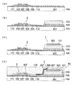
図2(a)は、PIN型PD1と読み出し用TFT2とで構成される画素がマトリクス状に複数個配置されたイメージセンサ20及びPIN型PD1による電荷を読み出し用TFT2を通じて電圧として読み出すための駆動回路部21を備えた撮像装置22を模式的に示す回路図である。また、図1は、図2(a)に示すイメージセンサ20を製造する工程を絶縁性基板の上に読み出し用TFT2とPIN型PD1とで構成される1画素の断面で模式的に示す図である。
FIG. 2A shows an
図1(c)は、イメージセンサ20が完成した状態の1画素を示しており、1はPIN型PD、2は読み出し用TFTの部分を示しており、これらが積層された状態で画素が構成されている。
FIG. 1C shows one pixel in a state in which the
100はガラス等の絶縁性基板、103はゲート電極、105はSiN、SiO2等のゲート絶縁層、107はアモルファスシリコン(a−Si)等の半導体層、109はオーミックコンタクト層、111はソース電極、112はドレイン電極、115はSiN、SiO2、BCB(Benzo Cyclo Butene)、PI(ポリイミド)等のパッシベーション層(平坦化層)、117はコンタクトホール、119は画素電極、121はN型半導体層、123はa−Si等のI型半導体層、125はP型半導体層、127はITO、SnO2等の透明導電性材料からなる共通電極、129はSiN、PI(ポリイミド)等のパッシベーション膜である。 100 is an insulating substrate such as glass, 103 is a gate electrode, 105 is a gate insulating layer such as SiN or SiO 2 , 107 is a semiconductor layer such as amorphous silicon (a-Si), 109 is an ohmic contact layer, and 111 is a source electrode , 112 are drain electrodes, 115 is a passivation layer (planarization layer) such as SiN, SiO 2 , BCB (Benzo Cyclo Butene), PI (polyimide), 117 is a contact hole, 119 is a pixel electrode, and 121 is an N-type semiconductor layer , 123 is an I-type semiconductor layer such as a-Si, 125 is a P-type semiconductor layer, 127 is a common electrode made of a transparent conductive material such as ITO or SnO 2 , and 129 is a passivation film such as SiN or PI (polyimide). is there.
ゲート電極103、ゲート絶縁膜105、半導体層107、オーミックコンタクト層109,ソース電極111及びドレイン電極112は読み出し用TFT2を構成する。
The
P型半導体層125、I型半導体層123及びN型半導体層121は、PIN型PD1を構成している。このPIN型PD1の透明電極層127はイメージセンサ20を構成する全てのPIN型PDにバイアスを印加するための共通電極である。また画素電極119と読み出し用TFT1のドレイン電極112とは、例えば、画素電極119と同時に設けることができるコンタクトホール117に設けられた電極により接続されている。
The P-
次に本実施の形態におけるPIN型PDを用いた撮像装置の製造に関して図1及び図2を参照して説明する。 Next, manufacturing of an imaging device using the PIN type PD in this embodiment will be described with reference to FIGS.
絶縁性基板100の上に、導電層を設け、公知のフォトリソグラフィー(レジスト塗布、露光、現像)及びエッチング処理により、読み出し用TFT2のゲート電極103及びゲートバス3a,3b,・・・3cを形成する。
A conductive layer is provided on the insulating
上記のゲート電極103及びゲートバス3a,3b,・・・3cは、導電性材料であれば特に限定されず、電極や配線(バス)としての導電性が十分確保できるものであればよい。例えば、Al、Cr、Ag、Moやこれらにドーピングした材料等を挙げることができる。導電層を形成する方法は、一般的な蒸着法で良く、例えば、真空蒸着やスパッタリング等の方法により形成することができる。
The above-described
次にゲート絶縁層105、a−Si等の半導体層107、オーミックコンタクト層109をプラズマCVD等により順次積層する。オーミックコンタクト層109、半導体層107をドライエッチング処理することで、読み出し用TFT2の島状領域を形成することができる。
Next, a
次に導電層をスパッタリング法等により積層し、公知のフォトリソグラフィー(レジスト塗布、露光、現像)及びエッチング処理により、読み出し用TFT2のソース電極111、ドレイン電極112、ソースバス4a,4b,・・・4cを形成する。また、同一レジストにより、オーミックコンタクト層109を、ドライエッチング処理にて除去することで、読み出し用TFT2のソース電極111−ドレイン電極112間のギャップ部を形成することができる。
Next, a conductive layer is laminated by a sputtering method or the like, and the
上記のソース電極111、ドレイン電極112及びソースバス4a,4b,・・・4cは、導電性材料であれば特に限定されず、電極や配線(バス)としての導電性が十分確保できるものであればよい。例えば、Al、Cr、Ag、Moやこれらにドーピングを加えた材料等が挙げることができる。導電層を形成する方法は、一般的な蒸着法で良く、例えば、真空蒸着やスパッタリング等の方法により形成することができる。
The
次に、SiN、SiO2、BCB、PI等の絶縁性のパッシベーション層115をプラズマCVD等により積層する。公知のフォトリソグラフィー処理及びエッチング処理により、コンタクトホール117を形成する。これで、図1(a)に示す読み出し用TFT2が完成するが、製造方法は上述に限定される必要はなく、公知の方法で良い。
Next, an insulating
次に、図1(b)に示すPIN型PD1の画素電極119を形成する。画素電極の厚みは、特に限定されることはなく、実用的な観点から10nmから1000nm程度とすれば良く、50nmから500nmが好ましい。画素電極119は、原料がホストとドーパントとから構成される。ホストは、導電性材料であれば特に限定されることはなく、例えば、金属材料であればAl、Cr、Mo、Ag、Ag/Zn(AgとZnとの合金)、Au、Au/Cr(AuとCrとの合金)等が挙げられ、また後述の透明電極となる透明導電性材料、例えば、ITO(インジウム錫酸化物)等とすることもできる。これらホストにドーピングされるドーパントは、後述のI型半導体に拡散(移行)することで、I型半導体の拡散された部分をN型半導体にするものであれば特に限定されることはない。例えば、I型半導体がIV族の材料、例えば、アモルファスシリコン(a−Si)であれば、ドーパントをV族の、例えば、リン(P)、窒素(N)等とすることで、a−SiからなるI型半導体をN型半導体とすることが出来る。また、PIN型PD1を構成する際に積層順を逆にしたい場合等でI型半導体をP型半導体にする場合は、III族の、例えば、ボロン(B)、アルミニウム(Al)等とすることで、a−SiからなるI型半導体をP型半導体とすることが出来る。また、I型半導体がIII−V族の材料、例えば、化合物半導体のGaAsであれば、ドーパントをVI族の、例えば、酸素(O)等、II族の、例えば、亜鉛(Zn)等とすることで、I型半導体層(GaAs)をそれぞれN型半導体、P型半導体とすることが出来る。
Next, the
画素電極119の形成方法は、まず、画素電極119となる導電層を形成する。導電層の形成方法は、特に限定されることはなく、例えば、スパッタリング法、CVD法、PLD法(パルスレーザー蒸着法)等が挙げられる。例えば、スパッタリング法であれば、ホストとなる原料を含むターゲットを用いて、ドーパントとなる原料を含むガスを導入することで可能となる。
As a method for forming the
導入するガスとしては、以下が挙げられ、ホストに合わせて適宜選択すればよい。I型半導体をIV族のa−Siとする場合、N型半導体を形成することができるドーピングガスとしては、V族元素と炭素、水素、塩素、フッ素などからなる化合物を用いることができる。その例を挙げれば、フォスフィン(PH3)、トリメチルホスフィン((CH3)3P)、アルシン(AsH3)、ジエチルアルシン((C2H5)2AsH)、アンモニア(NH3)などが挙げられる。 Examples of the gas to be introduced include the following, and may be appropriately selected according to the host. When the I-type semiconductor is a Group IV a-Si, as a doping gas capable of forming the N-type semiconductor, a compound composed of a V-group element and carbon, hydrogen, chlorine, fluorine, or the like can be used. Examples thereof include phosphine (PH 3 ), trimethylphosphine ((CH 3 ) 3 P), arsine (AsH 3 ), diethylarsine ((C 2 H 5 ) 2 AsH), ammonia (NH 3 ), and the like. It is done.
また、P型半導体を形成することができるドーピングガスとしては、III族元素と炭素、水素、塩素、フッ素などからなる化合物を用いることができる。これらの例を掲げれば、ジボラン(B2H6)、トリメチルボロン((CH3)3B)、ジメチルアルミニウム((CH3)2AlH)、トリメチルアルミニウム((CH3)3Al)などが挙げることが出来る。 Further, as a doping gas capable of forming a P-type semiconductor, a compound composed of a group III element and carbon, hydrogen, chlorine, fluorine, or the like can be used. Examples of these include diborane (B 2 H 6 ), trimethylboron ((CH 3 ) 3 B), dimethylaluminum ((CH 3 ) 2 AlH), and trimethylaluminum ((CH 3 ) 3 Al). I can list them.
上述の導電層の形成後、公知のフォトリソグラフィー処理及びエッチング処理により上述の導電層をパターニングすることで画素電極119を形成することができる。
After the formation of the conductive layer, the
次に、I型半導体層123及びP型半導体層125を形成する。形成方法は、公知の方法で良く、プラズマCVD法、触媒CVD法、HWCVD法(Hot−Wire−CVD)等が挙げられる。例えば、ホストをITO、導入ガスをフォスフィン(PH3)として形成してパターニングすることで画素電極119を形成した後、I型半導体層123としてI型a−Si層を積層形成した場合、画素電極119の上に積層されたI型a−Si層は、画素電極119が含むドーパンであるリン(P)がI型a−Si層に拡散する。従って、リン(P)が拡散したI型a−Siは、N型a−Siとなることから、I型a−Si層123のうち、画素電極119が接する部分及びその近傍は、N型a−Si層121となる。また、画素電極119が画素毎に分離されている状態にパターニングされていることから、N型a−Si層121は、画素毎に分離する工程を別途設けることなく、画素ごとに分離されている状態とすることができる。尚、I型半導体層123の厚みは、例えばa−Siとする場合、光吸収量から決めれば良く、可視光の範囲(約400nm〜750nmの範囲)であれば、100nmから5μm程度で良く、300nmから500nmの範囲が好ましい。
Next, an I-
上述のようにN型a−Si層121、I型a−Si層123及びP型a−Si層125を形成することでPIN型PD1を完成することができる。
By forming the N-
上述のPIN型PD1において、P型a−Si層125、I型a−Si層123、N型a−Si層121は、例えば、真空を破って成膜装置の外に取り出し、例えば、エッチング処理等によりN型a−Si層を画素毎に分離した状態にする必要がなく、成膜装置内で連続して成膜され、形成された各層の界面が連続した状態とすることができる。従って、各層の界面での欠陥の発生や不純物の混入を十分に抑えることができることから、暗電流の少ないPIN型PD1を形成できることになる。
In the above-described PIN type PD1, the P-
次に、バイアスの印加を可能とする共通電極127をP型a−Si層125の上に積層する。共通電極127は、光を入射する必要があることから、透明導電性材料であれば特に限定されることはなく、例えば、CuI、ITO、SnO2、IZO等の透明導電性材料が挙げられる。また、IDIXO(商品名、出光興産株式会社製)等非晶質で透明導電膜を作製可能な材料を用いてもよい。これらの透明導電性材料を用いて共通電極127を形成する方法は、特に限定されることはなく、公知の蒸着法やスパッタリング法等の方法を用いることができる。
Next, a
次に、パッシベーション膜129を、上述と同様に、更に積層することで、イメージセンサ20が完成する(図1(c))。更に、イメージセンサ20と、例えば、フレキシブル基板(図示しない)等を用いて、図2(a)に示す様に、ゲートドライバIC6が実装された基板、読み出しIC7が実装された基板等の駆動回路部21と接続することで、撮像装置22を完成させることができる。
Next, the
また、例えば、図1(d)に示す様に、パッシベーション膜129の上に放射線を光に変換する波長変換手段であるシンチレーター(蛍光体層)131、更にパッシベーション膜133を積層形成することで、イメージセンサ20は、放射線撮像装置に対応可能とすることができる。
Further, for example, as shown in FIG. 1 (d), a scintillator (phosphor layer) 131, which is a wavelength converting means for converting radiation into light, is laminated on the
シンチレーター131は、Gd2O2S,CsI(沃化セシウム)等を真空蒸着、CVD等で形成することができる。ここではシンチレーターをイメージセンサ20の上に直接積層しているが、例えば、別途ガラス等の基板の上にシンチレーターを設けてパッシベーション層で保護することでなる蛍光体板(図示しない)を、図1(c)で示すパッシベーション膜129まで製造したイメージセンサ20に貼り合わせた構成とすることもできる。
The
上述のシンチレーターを有するイメージセンサ20と、上述と同様に、フレキシブル基板等を用いて、図2(a)に示す様に、ゲートドライバIC6が実装された基板及び読み出しIC7が実装された基板と接続し、全体をケースに入れることでFPDを完成することができる。尚、ケース内に内蔵される上述の様なICで、X線等の放射線の影響を受ける場合は、鉛板等を設けて保護するのが好ましい。
As shown in FIG. 2A, the
上述のシンチレーターを備えた撮像装置の動作に関して図2を用いて説明する。撮像装置22は、放射線を可視光に変換する蛍光体層(図示しない)と、可視光を電気信号に変換する光電変換素子であるPIN型PD、TFTを用いた読み出し回路を絶縁性基板の上に形成したイメージセンサ20及び駆動回路部21との組み合わせで構成される。
The operation of the imaging device including the above scintillator will be described with reference to FIG. The
図2(a)において、1はPIN型PD、2は読み出し用TFTで、読み出し用TFT2のソースはソースバス4a,4b,・・・4cへ接続され、ドレインはPIN型PD1のカソードに接続され、ゲートはゲートバス3a,3b,・・・3cへ接続されている。PIN型PD1のアノードはバイアス線5に接続され、バイアス線5はバイアス電源8に接続され、負のバイアス電圧が印加されている。ゲートバス3a,3b,・・・3cは、それぞれゲートドライバIC6の出力端子G1,G2,・・・GNに接続され、ソースバス4a,4b,・・・4cは、それぞれ読み出しIC7の出力端子S1,S2,・・・SMに接続されている。このイメージセンサ20は、PIN型PD1および読み出し用TFT2のそれぞれ1個の組み合わせで1つの画素を形成し、合わせてN行×M列の画素を有している。
In FIG. 2A, 1 is a PIN type PD, 2 is a readout TFT, the source of the
ゲートドライバIC6はその出力端子G1,G2,・・・GNにゲートバス3a,3b,・・・3cが接続されており、正の電圧を順に出力しゲートバス3a,3b,・・・3cを走査する。読み出しIC7はその出力端子S1,S2,・・・SMにソースバス4a,4b,・・・4cが接続されており、正の電圧を出力する。また、読み出しIC7の出力端子S1,S2,・・・SMには、それぞれ電荷−電圧変換回路を備えており、ソースバス4a,4b,・・・4cに流れ出した電荷の量を電圧に変換する機能を有している。
An output terminal G 1 gate driver IC6 is, G 2, ··· G N to the
蛍光体層(図示しない)は、上述のイメージセンサ20を覆い、蛍光体層で発生した可視光がPIN型PD1に入射するように構成されている。
A phosphor layer (not shown) covers the above-described
撮像装置22の動作を、図2(a)に示す回路図、及び図2(b)に示すタイミングチャートを用いて説明する。図2(b)で11,12,13は、それぞれゲートドライバIC6の出力端子G1,G2,・・・GNの電圧を示す。ゲートバス3a,3b,・・・3cがハイになるとそのゲート線に接続されているTFT2がすべてオン状態となる。このとき、読み出しIC7の出力端子S1,S2,・・・SMからは正の電圧がソースバス4a,4b,・・・4cに出力されているため、オンしたTFT2に接続されているPIN型PD1は逆バイアスされ、PIN型PD1の容量には電荷が充電される。このときPIN型PD1に流れ込む充電電流、すなわち読み出しIC7の出力端子S1,S2,・・・SMからソースバス4a,4b,・・・4cに流れ込む電荷は、読み出しIC7で電荷−電圧変換され、電圧として読み出される。ゲートバス3a,3b,・・・3cがロウになると、そのゲート線に接続されているTFT2はすべてオフし、そのTFT2に接続されているPIN型PD1の充電された電荷は保持される。
The operation of the
図2(b)で初期化走査と示された期間は、放射線像の撮影に備えて、すべての光電変換素子1を充電するための走査期間である。図2(b)の14は放射線の曝射を示し、ハイになっている期間が放射線の曝射が行われている期間を示す。図2(b)に示すように、放射線の曝射は、撮像装置9の初期化走査の終了後に行われる。放射線が曝射されると、放射線の照射を受けた蛍光体層が蛍光を発し、この蛍光を受光したPIN型PD1は、その中で電子−ホール対が発生し、充電されていた電荷を放電する。このため、PIN型PD1に充電されていた電荷は、受光量に応じて発生した電子−ホール対の分だけ減少する。
A period indicated as initialization scanning in FIG. 2B is a scanning period for charging all the
放射線の曝射に続いて、図2(b)に示す読み出し走査が行われる。読み出し走査の時、読み出しIC7から読み出される電荷−電圧変換された電圧は、放射線曝射の時、光電変換素子1から放電により消滅した電荷に相当する。従って、蛍光体層に入射した放射線による画像が、電圧として二次元的に読み出すことができる。
Subsequent to the radiation exposure, the readout scanning shown in FIG. 2B is performed. The charge-voltage converted voltage read from the read
図2(b)のTiは積分期間を示しており、蛍光体層から発生した可視光による電子−ホール対がこの期間においてPIN型PD1で積分される。従って、積分期間Tiは、放射線の曝射期間および蛍光体層の発光期間を含むようにするのが好ましく、また、例えば蛍光体層を設けていない場合、可視光による露光期間も同じとするのが好ましい。 Ti in FIG. 2B indicates an integration period, and electron-hole pairs generated by visible light generated from the phosphor layer are integrated by the PIN PD1 during this period. Therefore, it is preferable that the integration period Ti includes the radiation exposure period and the light emission period of the phosphor layer. For example, when the phosphor layer is not provided, the exposure period by visible light is the same. Is preferred.
第2の実施の形態として、絶縁性基板の上に読み出し用TFTを形成し、別のガラス基板の上にPIN型PDを形成した後、両者を重ねて貼り合わせることでなる撮像装置について説明する。 As a second embodiment, an image pickup apparatus will be described in which a readout TFT is formed on an insulating substrate, a PIN-type PD is formed on another glass substrate, and then both are stacked and bonded together. .
図3(c)は、イメージセンサ30が完成した状態の1画素を示している。1は基板203の上に形成されているPIN型PD、2は基板100の上に形成されている読み出し用TFTであり、イメージセンサ30は、PIN型PD1と読み出し用TFT2とが重ねて貼り合わせた状態で構成されている。尚、図3で示す図1と同じ符号は、同じものを示している。
FIG. 3C shows one pixel in a state where the
次に撮像装置の製造に関して図3を参照して説明する。まず、読み出し用TFTを絶縁性基板100の上に形成し、これをTFT基板部3Aとする。TFT基板部3Aは、図3(a−1)が図1(a)と同じであり、第1の実施の形態で説明したパッシベーション膜115を形成後、コンタクトホール117を設けるまでは同じとすることができる。
Next, manufacturing of the imaging device will be described with reference to FIG. First, the readout TFT is formed on the insulating
この後、コンタクトホール117に読み出し用TFT2を設けたTFT基板部3A(図3(a−2))と後述のPIN型PD1を設けたPD基板部3B(図3(b−3))とを電気的に接続するためのバンプ(突起電極)201を形成する。
Thereafter, a
次に、PIN型PDを別のガラス等の透明な絶縁性基板203の上に形成する。絶縁性基板203の上にPIN型PDにバイアスを印加するための共通電極となる透明電極127、P型半導体層125、I型半導体層123を積層して設ける(図3(b−1))。これに関しては、積層順が異なるだけで、第1の実施の形態で示したものと同じとすることができる。
Next, a PIN type PD is formed on another transparent insulating
次に、画素電極119をI型半導体層123の上に形成する。I型半導体層123の上にリフトオフを行うためのレジストを塗布し、公知のフォトリソグラフィー処理及びエッチングを行い、画素電極119を形成するためのレジストのパターニングを行う。この後、画素電極119となる導電膜を形成した後、リフトオフすることで画素電極119を形成する(図3(b−2))。この導電膜は、第1の実施の形態で説明した画素電極119と同じホストとドーパントとから構成されており、I型半導体層123の上に画素電極119を形成することで、第1の実施の形態と同じく、画素電極119が有するドーパントが拡散され、I型半導体をN型半導体にすることが出来る。従って、PIN型PD1を完成することができる。
Next, the
次に、画素電極119の上にパッシベーション膜207を設けた後、バンプ(突起電極)205を設ける。これでPD基板部3Bを完成することができる(図3(b−3))。パッシベーション膜207は、特に限定することはなく、例えば、パッシベーション膜129と同じとして良い。
Next, after providing a
次に、先に製造したTFT基板部3Aのドレイン電極112とPD基板部3Bの画素電極119とをバンプ201と205とを電気的に接続してイメージセンサ30を完成することができる(図3(c))。
Next, the
バンプ201及び205は、インジウム(In)、金(Au)又は導電性樹脂等で形成される突起状の電極であり、両バンプ間を結合する方法は、電気的に接続されていれば良く、例えば、導電性樹脂の場合、加熱及び/又は紫外線照射や、またインジウム(In)等の低融点材料では加熱溶着、また、接触した状態で樹脂を流し込むことで固定するといった方法を挙げることができる。
The
尚、シンチレーター、図2で示したIC6及びIC7が実装されている基板等から構成される駆動回路部21とイメージセンサ30とで構成される撮像装置に関しては、第1の実施の形態と同様となる。
Note that the image pickup apparatus including the scintillator, the
第3の実施の形態として、絶縁性基板の同一面の上に読み出し用TFTとPIN型PDを形成してなる撮像装置について図4を参照して説明する。尚、図4で示す図1と同じ符号は、同じものを示している。 As a third embodiment, an image pickup apparatus in which a readout TFT and a PIN type PD are formed on the same surface of an insulating substrate will be described with reference to FIG. The same reference numerals as those in FIG. 1 shown in FIG. 4 denote the same components.
図4(a)は、第1の実施の形態と同様に形成された読み出し用TFT2を示している。すなわち、100はガラス等の絶縁性基板、103はゲート電極、105はゲート絶縁層、107はa−Si等の半導体層、109はオーミックコンタクト層、111はソース電極、112はドレイン電極である。ここで、PIN型PDを基板100の上に形成するため、ソース電極111及びドレイン電極112の形成と同時にPIN型PD1の共通電極301も形成する。
FIG. 4A shows a
次に、PIN型PD1を構成するためのP型半導体層125、I型半導体層123を共通電極301の上に形成する。形成方法は、特に限定されることはなく、例えば、第1の実施の形態と同様にプラズマCVD法等を用いて各半導体層を積層形成した後、公知のフォトリソグラフィー処理及びエッチング処理を行い、図4(b)に示す様にP型半導体層125、I型半導体層123を画素となる形状に形成することができる。
Next, a P-
次に、画素電極303を形成する(図4(c))。画素電極303は、第1の実施の形態の画素電極119と同じく、ホストとドーパントとから構成される。また、画素電極303の大きさは、画素電極303を積層するI型半導体層123の上部の面の大きさより小さくすることが好ましい。I型半導体層123の上部の面の外周と画素電極303の外周との距離は、拡散されるドーパントの元素が到達しない距離とするのが好ましく、1μm以上とするのが好ましく、5μm以上とするのがより好ましい。
Next, the
I型半導体層123の上に画素電極303を形成することで、I型a−Si層123において、画素電極303が接する部分及びその近傍は、N型a−Si層121にすることができる。従って、P型半導体層125の上にI型半導体層123が積層され、I型半導体層123の上部にN型a−Si層121が形成されることで、PIN型PD1を完成することができる。
By forming the
上述のようにPIN型PD1を形成することで、第1の実施の形態と同様に、P型a−Si層、I型a−Si層、N型a−Si層は、連続して成膜されることになり、形成される各層の界面が連続した状態とすることができる。よって、各層の界面での欠陥の発生や不純物の混入を十分に抑えることができることから、暗電流の少ないPIN型PD1を形成できることになる。 By forming the PIN type PD1 as described above, the P-type a-Si layer, the I-type a-Si layer, and the N-type a-Si layer are continuously formed as in the first embodiment. As a result, the interface of each layer to be formed can be made continuous. Therefore, the occurrence of defects at the interface of each layer and the mixing of impurities can be sufficiently suppressed, so that the PIN type PD1 with a small dark current can be formed.
また、画素電極303にドープされたドーパントが拡散することで形成されるN型a−Si層は、画素電極303の大きさを画素電極303が積層されるI型半導体層123の上部の面より小さくすることで、結晶構造が不完全となっているPIN型PD1のエッチングされた側面に面していない状態とすることができる。従って、PIN型PD1を形成している側面からのリーク電流を抑えることが可能となり、その結果、暗電流の少ないPIN型PD1を形成できることになる。
In addition, the N-type a-Si layer formed by diffusing the dopant doped into the
画素電極303を形成した後、パッシベーション膜307、画素電極303とドレイン電極112とを接続する接続電極309、読み出し用TFT2とPIN型PD1とを保護するパッシベーション膜115を設けることでイメージセンサ40を完成することができる(図4(d))。
After the
尚、シンチレーター、図2で示したIC6及びIC7が実装されている基板等から構成される駆動回路部21とイメージセンサ40とで構成される撮像装置の動作に関しては、第1の実施の形態と同様となる。
The operation of the image pickup apparatus including the
第4の実施の形態として、I型半導体層の両側にI型半導体層をP型半導体層及びN型半導体層とすることが出来るドーパンがドーピングされた電極を設けることでPIN型PDを形成することに関して説明する。 As a fourth embodiment, a PIN-type PD is formed by providing dope-doped electrodes capable of making an I-type semiconductor layer a P-type semiconductor layer and an N-type semiconductor layer on both sides of an I-type semiconductor layer. This will be explained.
図5(a)は、ガラス等の絶縁性基板100の上に、第1の実施の形態と同様に、ゲート電極103、ゲート絶縁層105、a−Si等の半導体層107を形成する。その後、SiN、SiO2等のエッチングストップ層501を設ける(図5(a))。
In FIG. 5A, a
次に、導電層503を設け(図5(b))、その後、公知のフォトリソグラフィー処理及びエッチング処理を行いソース電極503s、ドレイン電極503d及びPIN型PDの画素電極503Kを形成する(図5(c))。この導電層503を、第1の実施の形態の画素電極119と同様に、ホストとドーパンとから構成する、例えば、リン(P)をドーパンとすることで、ソース電極503s及びドレイン電極503dに接する半導体層107に、N型半導体層505を形成することができることになり、この結果、このN型半導体層505が第1の実施の形態で形成したオーミックコンタクト層109と同じ機能である、ソース電極及びドレイン電極と半導体層107との接触抵抗を小さくする機能を果たすことができる。従って、オーミックコンタクト層を形成する工程を別途設ける必要がなく、製造を容易にすることができる。
Next, a
尚、絶縁材でなるエッチングストップ層501があるため、導電層503が半導体層107に接触することができないため、読み出し用TFTにおいてチャネル形成される部分は、ドーパントの拡散はなされない。よって、読み出し用TFT2はこれまで説明した他の実施の形態と同様に問題なく動作することができる。
Note that since there is an
次に、先に設けた画素電極503Kの上にI型半導体層123をプラズマCVD等により成膜した後、エッチング処理により画素の形状に形成する(図5(d))。その後、I型半導体をP型半導体とすることが出来るドーパン、例えば、ボロン(B)を含む共通電極507を形成する。共通電極507が含むドーパンがI型半導体層123に拡散することで、P型半導体層509を形成することができる。また、画素電極503Kが含むドーパンがI型半導体層123に拡散することで、N型半導体層121を形成することができる。従って、PIN型PD1を完成することができる。
Next, an I-
共通電極507の大きさは、第3の実施の形態の電極303と同様に、共通電極507を積層するI型半導体層123の上部の面の大きさより小さくすることで、リーク電流を抑えることが出来、結果として暗電流の少ないPIN型PD1を形成できることになる。また、P型半導体層及びN型半導体層を形成する工程を別途設ける必要がなく、製造を容易にすることができる。
Like the
次に、パッシベーション膜307、共通電極507にバイアスを印加するためのバイアス配線511、更にパッシベーション膜115を設けることで、イメージセンサ50を完成することが出来る(図5(e))。
Next, the
尚、シンチレーター及び図2で示したIC6及びIC7が実装されている基板等から構成される駆動回路部21とイメージセンサ40とで構成される撮像装置の動作に関しては、第1の実施の形態と同様となる。
The operation of the image pickup apparatus including the
これまでの説明した第1から第4の実施の形態において光電変換素子をI型半導体、P型半導体及びN型半導体から構成されるPIN型PDとしているが、I型半導体とP型半導体又はN型半導体のいずれかとから構成されるMIS型PDとすることができる。MIS型PDとする場合、図2(a)において、露光によりMIS型PD2に発生した正孔を次の露光までに消滅させるためのリフレッシュ回路(図示しない)を設けることで対応することができる。 In the first to fourth embodiments described so far, the photoelectric conversion element is a PIN type PD composed of an I-type semiconductor, a P-type semiconductor and an N-type semiconductor, but the I-type semiconductor and the P-type semiconductor or N MIS type PD composed of any one of the type semiconductors. The MIS type PD can be dealt with by providing a refresh circuit (not shown) for eliminating the holes generated in the MIS type PD2 by exposure until the next exposure in FIG.
これまで説明した実施の形態に沿って製造した撮像装置に関して説明する。以下で説明する実施例及び比較例で製造した全ての撮像装置が有するイメージセンサは、大きさ60mm×50mm、厚み0.7mmの無アルカリガラス(コーニング製 #1737)を基板とし、画素の大きさは105μm×160μm、画素数は480×240で2次元マトリクス状に配置されている。 An imaging device manufactured according to the embodiments described so far will be described. The image sensors included in all the imaging devices manufactured in the examples and comparative examples described below have a pixel size of 60 mm × 50 mm and a non-alkali glass (Corning # 1737) having a thickness of 0.7 mm as a substrate. Is 105 μm × 160 μm, the number of pixels is 480 × 240, and is arranged in a two-dimensional matrix.
(実施例1)
第1の実施の形態で説明した基板の上に読み出し用TFTの上にPIN型PDを積層された画素が2次元マトリクス状に配置されているイメージセンサを有する撮像装置を製造したことに関して図1に沿って説明する。
Example 1
With respect to manufacturing an imaging device having an image sensor in which pixels in which a PIN type PD is stacked on a readout TFT on a substrate described in the first embodiment are arranged in a two-dimensional matrix. It explains along.
ガラス基板100の上に、まず読み出し用TFTを作製した。ゲート電極となる導電膜としてMo(モリブデン)を成膜し、フォトリソグラフィ−処理及びエッチング処理によりゲート電極103を形成した。ゲート絶縁膜105として、SiO2成膜し、更に半導体層としてa−Si膜、オーミックコンタクト層としてN型a−Si膜を積層形成した後パターニングすることで半導体層107、オーミックコンタクト層109を形成した。
First, a readout TFT was fabricated on the
次に、導電膜としてMo膜を成膜後、フォトリソグラフィ−処理及びエッチング処理によりソース電極111及びドレイン電極112を形成した。これで読み出し用TFT2が完成したことになる。
Next, after forming a Mo film as the conductive film, the
次に、パッシベーション層115としてSiNをプラズマCVDで作製した後、フォトリソグラフィ−処理及びエッチング処理によりコンタクトホール117を設けた(図1(a))。
Next, after forming SiN by plasma CVD as the
次に、画素電極119を形成した。フォスフィン(PH3)を流量比5%含んだAr雰囲気でITO(SnO2 5質量%)ターゲットをスパッタリングすることで、厚さ0.2μmのリン(P)ドープのITO層を形成した。この時のスパッタリング条件は、圧力0.4Pa、パワー500W、基板温度200℃とした。この基板は、図1(a)で示すTFTが形成されたガラス基板である。このITO層をフォトリソグラフィ−処理及びエッチング処理して、画素電極119を形成した(図1(b))。このエッチング処理は、メタンガスと水素ガスを用いたドライエッチング処理とした。
Next, the
次に、光電変換素子であるPIN型PD1を形成した。プラズマCVD法により、I型a−Si層123とP型a−Si層125を連続して成膜した。
Next, PIN type PD1 which is a photoelectric conversion element was formed. An I-
次に、スパッタリング法によりITOを成膜して共通電極127を形成し、更にプラズマCVD法により、SiNを積層してパッシベーション層129を形成した(図1(c))。これで、イメージセンサJ1が完成したことになる。このイメージセンサJ1に、図2(a)で示すゲートドライバIC6が実装された基板及び読み出しIC7が実装された基板から構成される駆動回路部21を接続することで撮像装置とした。
Next, ITO was formed by sputtering to form a
(比較例1)
以下の説明以外は、実施例1と同じとしてイメージセンサH1を製造した。画素電極119を形成するときにフォスフィン(PH3)の供給をしなかった。また、プラズマCVD法により、I型a−Si層123を形成する前にN型a−Si層を形成した後、フォトリソグラフィ−処理及びエッチング処理を行いN型a−Si層を画素毎に分離するパターニングを行った。この後、I型a−Si層123以降を実施例1と同じとした。
(Comparative Example 1)
An image sensor H1 was manufactured as in Example 1 except for the following description. When the
(実施例1と比較例1との比較結果)
実施例1のイメージセンサJ1に光を照射することで動作することが確認できた。従って、画素電極119であるITOに存在するリン(P)がI型a−Si膜へと拡散し、画素電極付近のI型a−SiがN型a−Si層121になり、PIN型PD1を形成していることが確認できた。
(Comparison result between Example 1 and Comparative Example 1)
It was confirmed that the image sensor J1 of Example 1 was operated by irradiating light. Accordingly, phosphorus (P) present in the ITO that is the
また、図2で示した駆動回路部21を用いてイメージセンサJ1及びイメージセンサH1それぞれを光を当てない状態で駆動して、暗電流量を比較したところ実施例1のイメージセンサJ1の方が少ないことが確認できた。
Further, when the image sensor J1 and the image sensor H1 are driven in a state where no light is applied using the
(実施例2)
第2の実施の形態で説明した基板の上に読み出し用TFTの上にPIN型PDを積層された画素が2次元マトリクス状に配置されているイメージセンサを有する撮像装置を製造したことに関して図3に沿って説明する。
(Example 2)
Regarding manufacturing of an imaging device having an image sensor in which pixels in which a PIN type PD is stacked on a readout TFT on a substrate described in the second embodiment are arranged in a two-dimensional matrix. It explains along.
コンタクトホール117を設けるまで実施例1と同じとしてガラス基板100の上に読み出し用TFT2を形成した(図3(a−1))。次に、流動性電極材料であるPEDOT/PSS(ポリエチレンジオキシチオフェンとポリスチレンスルホン酸の錯体)を用いたスクリーン印刷法で導電性バンプ201を形成した(図3(a−2))。これでTFT基板部3Aを完成させた。
The
次に、ガラス基板203の上にPIN型PD1を形成した。まず、ガラス基板203の上にITOによる共通電極127、P型a−Si層125、I型a−Si層123を順次積層した(図3(b−1))。それぞれの形成方法は、実施例1と同じとした。
Next, a PIN type PD1 was formed on the
次に、画素電極119を形成した。まず、レジストをリフトオフによる画素電極119の形成を想定したパターニングした後、これも実施例1と同じく、フォスフィン(PH3)を流量比5%含んだAr雰囲気でITO(SnO2 5質量%)ターゲットをスパッタリングすることで、厚さ0.2μmのリン(P)ドープのITO層を形成した。この時のスパッタリング条件は、圧力0.4Pa、パワー500W、基板温度200℃とした。この基板は、図1(a)で示すTFT2が形成されたガラス基板である。ITO層を形成した後、リフトオフにて不要なITO層を除去してITOによる画素電極119を形成した(図3(b−2))。
Next, the
次に、プラズマCVD法により、SiNを積層してパッシベーション層207を形成した後、フォトリソグラフィ−処理及びエッチング処理にてバンプ用ホール形成し、上述と同じスクリーン印刷法で導電性バンプ205を形成した(図3(b−3))。これでPD基板部3Bを完成させた。
Next, after depositing SiN by plasma CVD method to form a
次に、TFT基板部3AとPD基板部3Bとを重ね合わせてバンプ201とバンプ205とが接触した状態で接着剤を用いて貼り合わせてイメージセンサJ2を完成させた(図3(c))。このイメージセンサJ2に、図2(a)で示すゲートドライバIC6が実装された基板及び読み出しIC7が実装された基板から構成される駆動回路部21を接続することで撮像装置とした。
Next, the
(比較例2)
以下の説明以外は、実施例2と同じとしてイメージセンサH2を製造した。プラズマCVD法により、I型a−Si層123を形成する後にN型a−Si層を形成し、この後、フォスフィン(PH3)の供給することなく画素電極119を形成した。この後、フォトリソグラフィ−処理及びエッチング処理を行い、画素電極119及びN型a−Si層を画素毎に分離するパターニングを行った。この後、パッシベーション層207及びバンプ205を設けた。
(Comparative Example 2)
An image sensor H2 was manufactured as in Example 2 except for the following description. After forming the I-
(実施例2と比較例2との比較結果)
実施例2のイメージセンサJ2が光を照射することで動作することが確認できた。従って、画素電極119であるITOに存在するリン(P)がI型a−Si膜へと拡散し、画素電極付近のI型a−SiがN型a−Si121になり、PIN型PD1を形成していることが確認できた。
(Comparison result between Example 2 and Comparative Example 2)
It was confirmed that the image sensor J2 of Example 2 was operated by irradiating light. Therefore, phosphorus (P) present in the ITO that is the
また、図2で示した駆動回路部21を用いてイメージセンサJ2及びイメージセンサH2それぞれを光を当てない状態で駆動して、暗電流量を比較したところ実施例2のイメージセンサJ2の方が少ないことが確認できた。
Further, when the image sensor J2 and the image sensor H2 are driven in a state where no light is applied using the
(実施例3)
第3の実施の形態で説明した絶縁性基板の同一面の上に読み出し用TFTとPIN型PDとで構成される画素が2次元マトリクス状に配置されているイメージセンサを有する撮像装置を製造したことに関して図4に沿って説明する。
(Example 3)
An imaging apparatus having an image sensor in which pixels including readout TFTs and PIN type PDs are arranged in a two-dimensional matrix on the same surface of the insulating substrate described in the third embodiment is manufactured. This will be described with reference to FIG.
ガラス基板100の上に実施例1と同じ方法で読み出し用TFTを形成した。ソース電極111及びドレイン電極112をパターニングにより形成する際に、同時に共通電極301も形成した(図4(a))。
A readout TFT was formed on the
次に、プラズマCVD法により、P型a−Si層とI型a−Si層とを連続して成膜した。この後、フォトリソグラフィー処理及びエッチング処理にて画素形状のP型a−Si層125とI型a−Si層123とを形成した(図4(b))。
Next, a P-type a-Si layer and an I-type a-Si layer were successively formed by plasma CVD. Thereafter, a pixel-shaped P-
次に、リフトオフ用のレジストを塗布し、画素電極を形成するためのパターニングを行った。ここで、画素電極のパターンは、I型a−Si層123の上面の大きさよりも小さくした。具体的には、I型a−Si層123の上面の外周より5μm内側とした。
Next, a lift-off resist was applied, and patterning for forming pixel electrodes was performed. Here, the pattern of the pixel electrode was made smaller than the size of the upper surface of the I-
次に、実施例1の画素電極119と同じリン(P)をドーパントとするITO層を形成した後、リフトオフを行うことでITOからなる画素電極303のパターニングを行った(図4(c))。
Next, after forming an ITO layer using the same phosphorus (P) as the dopant as the
次に、パッシベーション膜307を形成し、フォトリソグラフィー処理及びエッチング処理にて画素電極303及びドレイン電極112の位置にコンタクトホールを設けた。その後、アルミニウム(Al)をスパッタリング法で成膜し、その後パターニングを行うことで接続電極309を形成することで、読み出し用TFT2とPIN型PD1とを電気的に接続した。この後、パッシベーション膜115を形成してイメージセンサJ3を完成させた(図4(d))。このイメージセンサJ3に、図2(a)で示すゲートドライバIC6が実装された基板及び読み出しIC7が実装された基板から構成される駆動回路部21を接続することで撮像装置とした。
Next, a
(比較例3)
以下の説明以外は、実施例3と同じとしてイメージセンサH3を製造した。プラズマCVD法により、I型a−Si層を形成した後にN型a−Si層を積層した後、フォトリソグラフィ−処理及びエッチング処理を行いP型a−Si層、I型a−Si層及びN型a−Si層を画素毎に分離された画素形状にするパターニングを行った。次に、フォスフィン(PH3)の供給することなく画素電極303を形成した。
(Comparative Example 3)
An image sensor H3 was manufactured as in Example 3 except for the following description. After forming an I-type a-Si layer by plasma CVD, an N-type a-Si layer is stacked, and then a photolithography process and an etching process are performed to perform a P-type a-Si layer, an I-type a-Si layer, and an N-type layer. Patterning was performed so that the mold a-Si layer was separated into pixels. Next, the
(実施例3と比較例3との比較結果)
実施例3のイメージセンサJ3が光を照射することで動作することが確認できた。従って、画素電極303であるITOに存在するリン(P)がI型a−Si層へと拡散し、画素電極付近のI型a−SiがN型a−Si121になり、PIN型PD1を形成していることが確認できた。
(Comparison result between Example 3 and Comparative Example 3)
It was confirmed that the image sensor J3 of Example 3 was operated by irradiating light. Accordingly, phosphorus (P) present in the ITO that is the
また、図2で示した駆動回路部21を用いてイメージセンサJ3及びイメージセンサH3それぞれを光を当てない状態で駆動して、暗電流量を比較したところ実施例3のイメージセンサJ2の方が少ないことが確認できた。これは、実施例3においてPIN型PDの側面からのリーク電流が抑えられているためと考えられる。
Further, when the image sensor J3 and the image sensor H3 are driven in a state where no light is applied using the
(実施例4)
第4の実施の形態で説明した絶縁性基板の同一面の上に読み出し用TFTとPIN型PDとで構成される画素が2次元マトリクス状に配置されているイメージセンサを有する撮像装置を製造したことに関して図5に沿って説明する。
Example 4
An imaging apparatus having an image sensor in which pixels formed of readout TFTs and PIN type PDs are arranged in a two-dimensional matrix on the same surface of the insulating substrate described in the fourth embodiment is manufactured. This will be described with reference to FIG.
ガラス基板100の上に実施例1と同じく半導体層107まで形成し、半導体層107の上にエッチングストップ層501としてSiNを形成した(図5(a))。
The
次に、実施例1と同じドーパントをリン(P)とするITOからなる導電膜503を成膜する(図5(b))。このリン(P)がドープされた導電膜503であるITOをフォトリソグラフィー処理及びエッチング処理して画素電極503K、ソース電極503及びドレイン電極503dを形成した(図5(c))。
Next, a
次に、プラズマCVD法により、I型a−Si膜を成膜した後、フォトリソグラフィー処理及びエッチング処理することで画素形状のI型a−Si層123を形成した(図5(d))。
Next, after forming an I-type a-Si film by plasma CVD, a pixel-shaped I-
次に、リフトオフ用のレジストを塗布し、共通電極507を形成するためのパターニングを行った。ここで、画素電極のパターンは、I型a−Si層123の上面の大きさよりも小さくした。具体的には、I型a−Si層123の上面の外周より5μm内側とした。
Next, a lift-off resist was applied, and patterning for forming the
次に、共通電極507を形成した。ジボラン(B2H6)を流量比で5%含んだAr雰囲気でITOをスパッタリングし、厚さ200nmのボロン(B)ドープのITOを形成した。スパッタリング条件は、ITO(SnO2 5質量%)ターゲットを用い、圧力0.4Pa、パワー500W、基板温度200℃とした。この基板は、図5(d)で示すI型a−Si層123が形成されているガラス基板である。ITO層を形成した後、リフトオフを行うことでITOからなる共通電極507を形成した。
Next, the
次に、パッシベーション膜307を形成し、フォトリソグラフィー処理及びエッチング処理にて共通電極507の位置にバイアス配線511のためのコンタクトホールを設けた。その後、アルミニウム(Al)をスパッタリング法で成膜し、その後パターニングを行うことでバイアス配線511を形成した。この後、パッシベーション膜115を形成した(図5(e))。これで、イメージセンサJ4を完成させた。このイメージセンサJ4に、図2(a)で示すゲートドライバIC6が実装された基板及び読み出しIC7が実装された基板から構成される駆動回路部21を接続することで撮像装置とした。
Next, a
実施例4のイメージセンサJ4が光を照射することで動作することが確認できた。従って、画素電極503KであるITOに存在するリン(P)がI型a−Si層へと拡散し、画素電極付近のI型a−SiがN型a−Si121になり、また共通電極507であるITOに存在するボロン(B)がI型a−Si層へと拡散し、共通電極付近のI型a−SiがP型a−Si121になることでPIN型PD1が形成され問題なく動作することが確認できた。
It was confirmed that the image sensor J4 of Example 4 was operated by irradiating light. Accordingly, phosphorus (P) present in the ITO that is the pixel electrode 503K diffuses into the I-type a-Si layer, and the I-type a-Si near the pixel electrode becomes the N-
また、図2で示した駆動回路部21を用いてイメージセンサJ4を光を当てない状態で駆動したところ暗電流量は実施例3のイメージセンサJ3とほぼ同程度であることが確認できた。
Further, when the image sensor J4 was driven without applying light using the
(実施例5)
実施例1で製造したイメージセンサJ1のパッシベーション層129に重ねて、図1(d)に示す通り、シンチレーター131を設けた。蛍光体として沃化セシウム(CsI)を真空蒸着により形成し、更にパッシベーション層133を積層した。このようにして、イメージセンサJ1にシンチレーターを有するイメージセンサJ5を作製した。このイメージセンサJ5に、図2(a)で示すゲートドライバIC6が実装された基板及び読み出しIC7が実装された基板から構成される駆動回路部21を接続することで撮像装置とした。
(Example 5)
A
図2で示した駆動回路部21を用いてイメージセンサJ5を駆動しながらX線を暴射したところ読み出しICより信号が出力され問題なく動作することが確認できた。
When driving the image sensor J5 using the
1 PIN型PD
2 読み出し用TFT
20 イメージセンサ
100 絶縁性基板
103 ゲート電極
105 ゲート絶縁層
107 半導体層
109 オーミックコンタクト層
111 ソース電極
112 ドレイン電極
115、129、133 パッシベーション層
117 コンタクトホール
119 画素電極
121 N型半導体層
123 I型半導体層
125 P型半導体層
127 共通電極
131 蛍光体層
1 PIN type PD
2 Reading TFT
20
Claims (10)
前記電極の一方が前記I型半導体をN型半導体にするドーパントを含み、該ドーパントの移行により形成されるN型半導体層を有する構成、及び、前記電極の他方が前記I型半導体をP型半導体にするドーパントを含み、該ドーパントの移行により形成されるP型半導体層を有する構成、の少なくとも一方の構成を有することを特徴とする光電変換素子。 In a photoelectric conversion element in which both sides of an I-type semiconductor are sandwiched between electrodes,
One of the electrodes includes a dopant that makes the I-type semiconductor an N-type semiconductor, has an N-type semiconductor layer formed by migration of the dopant, and the other of the electrodes makes the I-type semiconductor a P-type semiconductor The photoelectric conversion element characterized by having at least one structure of the structure which has the P-type semiconductor layer formed by transfer of this dopant including the dopant to make.
前記光電変換素子は、前記薄膜トランジスタの上に積層されて電気的に接続されていることを特徴とする撮像装置。 A pixel comprising the photoelectric conversion element according to claim 1 or 2 and a thin film transistor provided on a substrate for reading a signal based on a charge by the photoelectric conversion element,
The photoelectric conversion element is stacked on the thin film transistor and electrically connected thereto.
前記光電変換素子は、前記薄膜トランジスタの上に重ねて貼り合わせて電気的に接続されていることを特徴とする撮像装置。 A pixel comprising: a photoelectric conversion element according to claim 1 or 2 provided on a substrate; and a thin film transistor provided on a substrate for reading a signal based on a charge by the photoelectric conversion element.
The image pickup device, wherein the photoelectric conversion element is electrically connected by being laminated on the thin film transistor.
前記光電変換素子と前記薄膜トランジスタとは、接続電極を介して電気的に接続されていることを特徴とする撮像装置。 A pixel comprising the photoelectric conversion element according to claim 1 and a thin film transistor that reads a signal based on a charge by the photoelectric conversion element, on the same surface of the substrate,
The imaging device, wherein the photoelectric conversion element and the thin film transistor are electrically connected through a connection electrode.
前記薄膜トランジスタが有するソース電極及びドレイン電極は、前記光電変換素子が有する前記ドーパントを含む前記電極と同一材料からなり、且つ前記ソース電極又は前記ドレイン電極の一方と前記ドーパントを含む前記電極とは一体であることを特徴とする撮像装置。 A pixel comprising the photoelectric conversion element according to claim 1 and a thin film transistor that reads a signal based on a charge by the photoelectric conversion element, on the same surface of the substrate,
The source electrode and the drain electrode included in the thin film transistor are made of the same material as the electrode including the dopant included in the photoelectric conversion element, and one of the source electrode or the drain electrode and the electrode including the dopant are integrated. There is an imaging apparatus.
前記I型半導体をN型半導体にするドーパントを含む第1の電極を形成し、該ドーパントを移行させてN型半導体層を有する工程、及び、前記I型半導体をP型半導体にするドーパントを含む第2の電極を形成し、該ドーパントを移行させてP型半導体層を有する工程の少なくとも一方の工程を有することを特徴とする光電変換素子の製造方法。 In a method for manufacturing a photoelectric conversion element in which both sides of an I-type semiconductor are sandwiched between electrodes,
Forming a first electrode containing a dopant that makes the I-type semiconductor an N-type semiconductor, transferring the dopant to have an N-type semiconductor layer, and a dopant making the I-type semiconductor a P-type semiconductor A method for manufacturing a photoelectric conversion element, comprising: forming a second electrode; transferring at least one of the steps of transferring the dopant and having a P-type semiconductor layer.
前記I型半導体をN型半導体にするドーパントを含む第1の電極を形成し、該ドーパントを移行させてN型半導体層を有する工程、及び、前記I型半導体をP型半導体にするドーパントを含む第2の電極を形成し、該ドーパントを移行させてP型半導体層を有する工程の少なくとも一方の工程を有し、前記第1の電極又は前記第2の電極を形成すると同時に前記第1の電極又は前記第2の電極と同一材料で前記ソース電極及び前記ドレイン電極を形成することを特徴とする撮像装置の製造方法。 Method for manufacturing an imaging device, comprising: a thin film transistor including a gate electrode, an insulating film, a semiconductor layer, a source electrode, and a drain electrode on a substrate; and a photoelectric conversion element having both sides of an I-type semiconductor sandwiched between electrodes In
Forming a first electrode containing a dopant that makes the I-type semiconductor an N-type semiconductor, transferring the dopant to have an N-type semiconductor layer, and a dopant making the I-type semiconductor a P-type semiconductor Forming at least one step of forming a second electrode and transferring the dopant to have a P-type semiconductor layer, and simultaneously forming the first electrode or the second electrode, the first electrode; Alternatively, the method for manufacturing an imaging device is characterized in that the source electrode and the drain electrode are formed of the same material as the second electrode.
Priority Applications (1)
| Application Number | Priority Date | Filing Date | Title |
|---|---|---|---|
| JP2006078578A JP2007258332A (en) | 2006-03-22 | 2006-03-22 | Photoelectric conversion element, photoelectric conversion element manufacturing method, imaging apparatus, imaging apparatus manufacturing method, and radiation imaging apparatus |
Applications Claiming Priority (1)
| Application Number | Priority Date | Filing Date | Title |
|---|---|---|---|
| JP2006078578A JP2007258332A (en) | 2006-03-22 | 2006-03-22 | Photoelectric conversion element, photoelectric conversion element manufacturing method, imaging apparatus, imaging apparatus manufacturing method, and radiation imaging apparatus |
Publications (1)
| Publication Number | Publication Date |
|---|---|
| JP2007258332A true JP2007258332A (en) | 2007-10-04 |
Family
ID=38632280
Family Applications (1)
| Application Number | Title | Priority Date | Filing Date |
|---|---|---|---|
| JP2006078578A Pending JP2007258332A (en) | 2006-03-22 | 2006-03-22 | Photoelectric conversion element, photoelectric conversion element manufacturing method, imaging apparatus, imaging apparatus manufacturing method, and radiation imaging apparatus |
Country Status (1)
| Country | Link |
|---|---|
| JP (1) | JP2007258332A (en) |
Cited By (7)
| Publication number | Priority date | Publication date | Assignee | Title |
|---|---|---|---|---|
| JP2009141361A (en) * | 2007-12-06 | 2009-06-25 | General Electric Co <Ge> | Cost-reduced pixel design for flat panel X-ray imagers |
| JP2009164598A (en) * | 2007-12-28 | 2009-07-23 | Dongbu Hitek Co Ltd | Image sensor and manufacturing method thereof |
| JP2009182134A (en) * | 2008-01-30 | 2009-08-13 | Fujifilm Corp | Method for manufacturing electromagnetic wave detection element |
| JP2011077184A (en) * | 2009-09-29 | 2011-04-14 | Fujifilm Corp | Detection element |
| JP2011181807A (en) * | 2010-03-03 | 2011-09-15 | Semiconductor Energy Lab Co Ltd | Method of fabricating photoelectric conversion device, and method of fabricating semiconductor device |
| KR101766595B1 (en) | 2016-10-04 | 2017-08-09 | 경희대학교 산학협력단 | X-ray detector having divided wavelength-conversion filter |
| JP2025026594A (en) * | 2015-04-09 | 2025-02-21 | 株式会社半導体エネルギー研究所 | Semiconductor Device |
-
2006
- 2006-03-22 JP JP2006078578A patent/JP2007258332A/en active Pending
Cited By (7)
| Publication number | Priority date | Publication date | Assignee | Title |
|---|---|---|---|---|
| JP2009141361A (en) * | 2007-12-06 | 2009-06-25 | General Electric Co <Ge> | Cost-reduced pixel design for flat panel X-ray imagers |
| JP2009164598A (en) * | 2007-12-28 | 2009-07-23 | Dongbu Hitek Co Ltd | Image sensor and manufacturing method thereof |
| JP2009182134A (en) * | 2008-01-30 | 2009-08-13 | Fujifilm Corp | Method for manufacturing electromagnetic wave detection element |
| JP2011077184A (en) * | 2009-09-29 | 2011-04-14 | Fujifilm Corp | Detection element |
| JP2011181807A (en) * | 2010-03-03 | 2011-09-15 | Semiconductor Energy Lab Co Ltd | Method of fabricating photoelectric conversion device, and method of fabricating semiconductor device |
| JP2025026594A (en) * | 2015-04-09 | 2025-02-21 | 株式会社半導体エネルギー研究所 | Semiconductor Device |
| KR101766595B1 (en) | 2016-10-04 | 2017-08-09 | 경희대학교 산학협력단 | X-ray detector having divided wavelength-conversion filter |
Similar Documents
| Publication | Publication Date | Title |
|---|---|---|
| CN101325207B (en) | Thin-film transistor array substrate for X-ray detector and x-ray detector | |
| CN101467256B (en) | Radiation imaging apparatus and radiation imaging system | |
| US7468531B2 (en) | Imaging apparatus and radiation imaging apparatus | |
| US20100054418A1 (en) | X-ray detecting element | |
| EP3451381B1 (en) | Array substrate for digital x-ray detector, digital x-ray detector including the same, and method for manufacturing the same | |
| US9093341B2 (en) | Imaging apparatus, manufacturing method thereof and imaging display system | |
| US11296139B2 (en) | Array substrate for digital X-ray detector and X-ray detector including the same | |
| CN102593164A (en) | Radiation imaging device, radiation imaging display system, and transistor | |
| US11209557B2 (en) | Array substrate for digital X-ray detector, digital X-ray detector including the same, and method for manufacturing the same | |
| JP5874201B2 (en) | Radiation imaging apparatus and radiation imaging display system | |
| US10651227B2 (en) | Array substrate for X-ray detector and X-ray detector including the same | |
| JP2000058808A (en) | 2D image detector | |
| JP2013157347A (en) | Imaging device and method of manufacturing the same, and imaging display system | |
| US11769783B2 (en) | Thin film transistor array substrate for digital X-ray detector device and digital X-ray detector device and manufacturing method thereof | |
| JP2004015002A (en) | Radiation imaging device | |
| JP2021110741A (en) | Manufacturing method of X-ray detector and X-ray detector | |
| US20090179242A1 (en) | Image sensor and method for manufacturing the same | |
| KR101103790B1 (en) | Radiography system and its manufacturing method | |
| KR20180036341A (en) | Digital x-ray detector for blocking hydrogen | |
| KR20210074705A (en) | Pin diode and thin film transistor array substrate for digital x-ray detector and the digital x-ray detector including the same |