JP2007281134A - Chip-type electronic component, its mounting board, and its mounting method - Google Patents
Chip-type electronic component, its mounting board, and its mounting method Download PDFInfo
- Publication number
- JP2007281134A JP2007281134A JP2006104232A JP2006104232A JP2007281134A JP 2007281134 A JP2007281134 A JP 2007281134A JP 2006104232 A JP2006104232 A JP 2006104232A JP 2006104232 A JP2006104232 A JP 2006104232A JP 2007281134 A JP2007281134 A JP 2007281134A
- Authority
- JP
- Japan
- Prior art keywords
- electronic component
- chip
- type electronic
- electrode
- substrate
- Prior art date
- Legal status (The legal status is an assumption and is not a legal conclusion. Google has not performed a legal analysis and makes no representation as to the accuracy of the status listed.)
- Pending
Links
- 238000000034 method Methods 0.000 title claims description 13
- 229910000679 solder Inorganic materials 0.000 claims abstract description 49
- 239000000758 substrate Substances 0.000 claims description 42
- 238000007747 plating Methods 0.000 claims description 15
- 230000032258 transport Effects 0.000 claims description 12
- 238000002844 melting Methods 0.000 claims description 8
- 230000008018 melting Effects 0.000 claims description 8
- 238000010438 heat treatment Methods 0.000 claims description 5
- 238000001816 cooling Methods 0.000 claims description 4
- 238000005476 soldering Methods 0.000 claims description 3
- 230000008569 process Effects 0.000 claims description 2
- 239000000463 material Substances 0.000 abstract description 8
- 238000004519 manufacturing process Methods 0.000 abstract description 5
- 239000000203 mixture Substances 0.000 abstract description 4
- 230000007547 defect Effects 0.000 abstract description 2
- 230000002093 peripheral effect Effects 0.000 abstract 1
- 239000003990 capacitor Substances 0.000 description 11
- 239000000853 adhesive Substances 0.000 description 5
- 230000001070 adhesive effect Effects 0.000 description 5
- 230000000694 effects Effects 0.000 description 4
- 238000009434 installation Methods 0.000 description 3
- 239000002184 metal Substances 0.000 description 3
- 230000002265 prevention Effects 0.000 description 3
- 239000000919 ceramic Substances 0.000 description 2
- 230000004907 flux Effects 0.000 description 2
- 230000005764 inhibitory process Effects 0.000 description 2
- 238000007726 management method Methods 0.000 description 2
- 239000000155 melt Substances 0.000 description 2
- 238000012545 processing Methods 0.000 description 2
- 238000009736 wetting Methods 0.000 description 2
- 230000008901 benefit Effects 0.000 description 1
- 230000008859 change Effects 0.000 description 1
- 239000011248 coating agent Substances 0.000 description 1
- 238000000576 coating method Methods 0.000 description 1
- 230000002950 deficient Effects 0.000 description 1
- 238000010586 diagram Methods 0.000 description 1
- 238000007598 dipping method Methods 0.000 description 1
- 239000006185 dispersion Substances 0.000 description 1
- 238000009826 distribution Methods 0.000 description 1
- 239000007788 liquid Substances 0.000 description 1
- 239000007769 metal material Substances 0.000 description 1
- 238000005457 optimization Methods 0.000 description 1
- 235000011837 pasties Nutrition 0.000 description 1
- 238000012805 post-processing Methods 0.000 description 1
- 238000004886 process control Methods 0.000 description 1
- 239000011347 resin Substances 0.000 description 1
- 229920005989 resin Polymers 0.000 description 1
- 230000004044 response Effects 0.000 description 1
- 230000000630 rising effect Effects 0.000 description 1
- 239000004065 semiconductor Substances 0.000 description 1
- 238000007711 solidification Methods 0.000 description 1
- 230000008023 solidification Effects 0.000 description 1
- 239000000126 substance Substances 0.000 description 1
Images


Landscapes
- Ceramic Capacitors (AREA)
Abstract
【課題】製造条件や材料組成の組合せによらずに、界面張力を減少させてツームストーン発生モーメントを小さくし、半田不良を防止できるようにした。
【解決手段】本発明は、電子部品本体の両側部に形成されて電子部品本体の内部電極に導通し、かつその一部が前記電子部品本体の上下面周囲に延設された外部電極30を備えたチップ型電子部品に31おいて、前記外部電極30の高さ方向上半部から電子部品本体の上面周囲にかけてその外周部をレジスト層20で被覆したものである。
【選択図】図1An object of the present invention is to reduce the interfacial tension to reduce the tombstone generation moment and prevent solder defects regardless of the combination of manufacturing conditions and material composition.
The present invention provides an external electrode 30 formed on both sides of an electronic component body and conducting to an internal electrode of the electronic component body, and a part of which extends around the upper and lower surfaces of the electronic component body. In the chip-type electronic component 31 provided, the outer peripheral portion is covered with a resist layer 20 from the upper half of the external electrode 30 in the height direction to the periphery of the upper surface of the electronic component main body.
[Selection] Figure 1
Description
本発明は、電子部品本体の両側部に形成されて電子部品本体の内部電極に導通し、かつその一部が前記電子部品本体の上下面周囲に延設された外部電極を備えたチップ型電子部品、その実装基板及びその実装方法に関するものである。 The present invention provides a chip-type electronic device that includes external electrodes formed on both sides of an electronic component body and conducting to internal electrodes of the electronic component body, and a part of which extends around the upper and lower surfaces of the electronic component body. The present invention relates to a component, its mounting board, and its mounting method.
最近では電子機器の小型化に伴う基板の小型化や、基板に対する実装の高密度化への要求により、電子部品のサイズをより小型化したチップ型電子部品が用いられている。このチップ型電子部品にあっては、部品本体の両側に露出する外部電極を電子部品本体の上下面周囲にまで延長したものである。 Recently, chip-type electronic components having a smaller electronic component size have been used in response to demands for miniaturization of substrates associated with miniaturization of electronic devices and high density mounting on substrates. In this chip-type electronic component, external electrodes exposed on both sides of the component main body are extended to the periphery of the upper and lower surfaces of the electronic component main body.
そして、この外部電極の底面側を、基板上に形成された基板電極(導電部)上に予め印刷された半田ペーストに接触させた状態で電子部品を基板上に設置し、次いで加熱することで、半田を溶融させて電気的に接続すると同時に電子部品を基板上に固定している。 Then, the electronic component is placed on the substrate while the bottom surface side of the external electrode is in contact with the solder paste printed in advance on the substrate electrode (conductive part) formed on the substrate, and then heated. The solder is melted and electrically connected, and at the same time, the electronic component is fixed on the substrate.
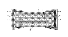
例えば図4は、チップ型コンデンサーの一例を示すもので、本体を構成するセラミック誘電体1の内部には一端を誘電体1の側部に露出させた左右複数の内部電極2が上下に所定の離間距離を保って対向配置されており、その外側面にそれぞれ前記各内部電極2に接続する外部電極内層3、外部電極中間層4、外部電極外層5を形成し、かつ各外部電極の上部及び下部を誘電体1の上面及び底面周囲に延在させている。
このチップ型コンデンサーの実際の大きさは、例えば長さ1.0mm、幅0.5mm、厚さ(高さ)0.5mmと極めて微小であり、その重量の極めて軽量である。
For example, FIG. 4 shows an example of a chip-type capacitor. Inside the
The actual size of this chip-type capacitor is extremely small, for example, a length of 1.0 mm, a width of 0.5 mm, and a thickness (height) of 0.5 mm, and its weight is extremely light.
ところで、前記のごとき微小部品を基板上に半田接合する際には、ツームストーンと称される一方の半田付け位置を基点とする立上がり現象が発生しやすく、接続不良の原因となっていた。
これは、溶融半田の界面張力が左右の接続位置でばらつきが生じ、これらによる影響を受けて一方の半田接続部に回転モーメントが生じやすいためである。
By the way, when soldering such a minute component on a substrate, a rising phenomenon called a tombstone, which is based on one soldering position, tends to occur, causing a connection failure.
This is because the interfacial tension of the molten solder varies between the left and right connection positions, and a rotational moment is likely to occur at one solder connection portion due to the influence of these.
図5はそのツームストーン現象を説明するためのもので、符号10は基板、符号11は基板10の部品設置位置の上に形成された一対の基板電極である。基板電極11上には図5(a)に示すように、印刷などにより半田ペースト12が所定の厚みに塗布され、次いで図5(b)に示すように、前記チップ型コンデンサーのごとき両側部に外部電極13を設けたチップ型電子部品14が半田ペースト12上に供給される。この状態では設置位置の半田ペースト12は押しのけられた状態となり、かつ電子部品の荷重Wと半田ペースト12中のフラックス成分による粘着力F1によってチップ型電子部品14は両基板電極11上に位置決め状態に仮固定される。
FIG. 5 is a diagram for explaining the tombstone phenomenon.
次いで、加熱することで半田ペースト12は溶融するが、このとき左右の半田ペースト12の溶融に僅かながらも時間差が生じた場合には、図5(c)に示すように、片側が溶融しても他方側が未だペースト状態にあることがある。この場合には、溶けた側の半田はその濡れにより外部電極13の側面に沿って這い上がり、略直角三角形状断面に形成される。そして、この這い上がった半田による縦方向荷重Fyと横方向荷重Fxとの合力が界面張力となり、この界面張力方向にチップ型電子部品14を傾けようとする回転モーメントM1が生じ、この回転モーメントM1が未溶融側半田ペーストの粘着力F1と荷重Wの合力である回転抑止モーメントM2より大となると、図5(d)に示すように、チップ型電子部品14は傾いてしまい、他方側の外部電極13が半田ペースト12から離間したまま所定時間遅れで加熱溶融され、冷却により固化してしまうのである。なお、溶融側における前記外部電極13の底面はそのまま回転抑止用の界面張力F’1として作用するが、高さ方向の接触面積より僅かな接触面積しかないため、有効ではなかった。
Next, the
今仮に以上のツームストーン現象の発生確率が0.1%程度であるとしても、例えば1つの基板に対し100個以上のチップ型電子部品が前記半田により接合している場合には製造された実装基板10枚のうち一枚は不良品となり、歩留りが低下するため、このツームストーン現象は実装密度を上げるための大きな障害となっていた。 Even if the probability of occurrence of the above tombstone phenomenon is about 0.1%, for example, when 100 or more chip-type electronic components are bonded to one substrate by the solder, Since one of the 10 substrates is a defective product and the yield is lowered, this tombstone phenomenon has been a major obstacle to increasing the mounting density.
ツームストーン現象の発生防止対策として、従来では、設計段階では部品が設置される左右の基板電極の均一化と、それにつながる導電パターンの均一化を図り、また、実装工程では印刷される半田量の適正化とばらつきの防止、及び左右の半田を極力同時に溶融させるためのリフロー条件設定など、如何に左右の溶融タイミングを合わせるかに主眼をおいて厳格な管理を行っていた。 As measures to prevent the occurrence of the tombstone phenomenon, conventionally, at the design stage, the left and right substrate electrodes on which components are installed are made uniform and the conductive pattern connected to them is made uniform. Strict management was performed focusing on how to match the right and left melting timings, such as optimization and prevention of dispersion, and setting of reflow conditions for melting the left and right solders as much as possible.
さらに、以上の工程管理と平行して、下記特許文献1では、外部電極及び半田の組成を工夫することでツームストーンを抑制できるようにしている。この技術では、接合材料が溶融するより先に外層電極を構成する金属が融解することで、液−液界面が形成され、界面張力を減少させてツームストーン発生モーメントを小さくするものである。
Further, in parallel with the above process control, in
しかしながら、前者の工程管理方法では、半田ペーストの印刷条件、炉内の加熱条件や温度分布が多少変動することによっても、ツームストーンの発生しやすい状態に変化するため、完全にツームストーン現象を排除することは出来なかった。 However, the former process management method completely eliminates the tombstone phenomenon because it changes to a state in which tombstones are likely to occur even if the solder paste printing conditions, heating conditions in the furnace, and temperature distribution change slightly. I couldn't do it.
また、特許文献1の方法では、外部電極と半田における材料組成の組合せが特定物質の組合せに限定され、その他は選択の自由度がないものとなる。
In the method of
本発明は、以上の課題を解決するものであり、前述のごとき製造条件や材料組成の組合せによらずに、界面張力を減少させてツームストーン発生モーメントを小さくし、半田不良を防止できるようにしたチップ型電子部品とその実装基板及び実装方法を提供するものである。 The present invention solves the above-described problems, and reduces the interfacial tension to reduce the tombstone generation moment and prevent solder defects regardless of the combination of manufacturing conditions and material composition as described above. The chip-type electronic component, its mounting substrate, and mounting method are provided.
前記課題を解決するため、本発明の第1の態様は、電子部品本体の両側部に形成されて電子部品本体の内部電極に導通し、かつその一部が前記電子部品本体の上下面周囲に延設された外部電極を備えたチップ型電子部品であって、前記外部電極の高さ方向上半部から上面周囲にかけてその外周がレジスト層で被覆されていることを特徴とするものである。 In order to solve the above-mentioned problem, a first aspect of the present invention is formed on both sides of an electronic component main body and is conducted to internal electrodes of the electronic component main body, and a part thereof is around the upper and lower surfaces of the electronic component main body. A chip-type electronic component having an extended external electrode, wherein the outer electrode is covered with a resist layer from the upper half in the height direction to the periphery of the upper surface.
本発明の第1の態様によれば、レジスト層の存在により、半田接合した際に、半田の這い上がり高さが従来の半分以下となり、両側での溶融時間差によるツームストーンを生じさせるモーメントも半減し、ツームストーンを原因とする接続不良などを防止できる。さらには製造メーカから提供される出来合のチップ型電子部品にレジストを塗布するという簡単な後加工を付加するだけで製作できるため、製造も簡単である。
なお、本発明で言う「高さ方向上半部」とは、厳密な意味合いで言う上半分でなく、ツームストーン防止性と、半田との接合性を勘案して適宜設定されるものであることは勿論である。
According to the first aspect of the present invention, due to the presence of the resist layer, when the solder is joined, the creeping height of the solder is less than half that of the prior art, and the moment causing the tombstone due to the difference in melting time on both sides is also halved. In addition, connection failures caused by tombstones can be prevented. Furthermore, since it can be manufactured simply by adding a simple post-processing of applying a resist to a ready-made chip-type electronic component provided by the manufacturer, the manufacturing is also simple.
In the present invention, the “upper half in the height direction” is not an upper half in a strict sense, and is appropriately set in consideration of tombstone prevention and solderability. Of course.
本発明の第2の態様は、電子部品本体の両側部に形成されて電子部品本体の内部電極に導通し、かつその一部が前記電子部品本体の上下面周囲に延設された外部電極を備えたチップ型電子部品であって、前記外部電極は多層構造に形成され、その最外層はその高さ方向上半部から上面周囲にかけてレジスト層で形成され、最外層の残りの部分は電極層で形成されていることを特徴とするものである。 According to a second aspect of the present invention, there is provided an external electrode formed on both sides of the electronic component main body and conducting to the internal electrode of the electronic component main body, and a part of which extends around the upper and lower surfaces of the electronic component main body. The external electronic electrode is formed in a multilayer structure, the outermost layer is formed of a resist layer from the upper half of the height direction to the periphery of the upper surface, and the remaining part of the outermost layer is an electrode layer It is characterized by being formed by.
本発明の第2の態様によれば、前記第1の態様と同様の作用効果が得られるほか、外部電極の最外層をレジスト層と電極層の厚さを同じにすることで、段差のない一様な外観構造に形成することができる。 According to the second aspect of the present invention, the same effect as the first aspect can be obtained, and there is no step by making the outermost layer of the external electrode the same thickness as the resist layer and the electrode layer. A uniform appearance structure can be formed.
本発明の第3の態様は、電子部品本体の両側部に形成されて電子部品本体の内部電極に導通し、かつその一部が前記電子部品本体の上下面周囲に延設された外部電極を備えたチップ型電子部品であって、前記外部電極は多層構造に形成され、その最外層はその高さ方向上半部から上面周囲にかけてメッキレジスト層で形成され、最外層の残りの部分は前記メッキレジスト層が形成された状態でメッキされた電極メッキ層で形成されていることを特徴とするものである。 According to a third aspect of the present invention, there is provided an external electrode formed on both sides of the electronic component main body and conducting to the internal electrode of the electronic component main body, and a part of which extends around the upper and lower surfaces of the electronic component main body. The external electrode is formed in a multilayer structure, the outermost layer is formed of a plating resist layer from the upper half in the height direction to the periphery of the upper surface, and the remaining part of the outermost layer is the chip-type electronic component It is characterized by being formed of an electrode plating layer plated in a state where a plating resist layer is formed.
本発明の第3の態様によれば、外部電極の最外層を成す前記電極メッキ層は、前記メッキレジスト層が形成された状態で最外層の残りの部分にメッキして形成されたものであるため、その製造が簡単である。 According to the third aspect of the present invention, the electrode plating layer forming the outermost layer of the external electrode is formed by plating the remaining portion of the outermost layer in a state where the plating resist layer is formed. Therefore, its manufacture is simple.
本発明の第4の態様は、チップ型電子部品がその外部電極を基板の電極部に半田接続されて実装されて成るチップ型電子部品の実装基板であって、前記チップ型電子部品は前記第1の態様から第3の態様のいずれかに記載されたチップ型電子部品であることを特徴とするものである。 According to a fourth aspect of the present invention, there is provided a chip-type electronic component mounting substrate in which the chip-type electronic component is mounted with its external electrodes soldered to the electrode portions of the substrate. A chip-type electronic component according to any one of the first to third aspects.
本発明の第4の態様によれば、ツームストーン防止効果に加え、従来の出来合のチップ型電子部品を基板上に実装する場合に比べて使用半田量も削減できるため、高密度実装を歩留り良く、かつ経済的に達成できる。 According to the fourth aspect of the present invention, in addition to the effect of preventing tombstones, the amount of solder used can be reduced as compared with the case where a conventional chip-type electronic component is mounted on a substrate. Can be achieved well and economically.
本発明の第5の態様は、基板電極の上に予め所定厚みで設けられる半田ペースト上に、前記第1の態様から第3の態様のいずれかに記載されたチップ型電子部品の外部電極の底面を位置決め状態に仮固定する工程と、仮固定状態で半田ペーストの溶融温度まで加熱する工程と、冷却により半田を固化させてチップ型電子部品の前記外部電極と前記基板電極を電気的に接続すると同時に当該チップ型電子部品を基板上に固定する工程とを有することを特徴とするチップ型電子部品の実装方法である。
本発明の第5の態様によれば、前記第4の態様と同様の作用効果が得られる。
According to a fifth aspect of the present invention, there is provided the external electrode of the chip-type electronic component according to any one of the first to third aspects, on a solder paste previously provided with a predetermined thickness on the substrate electrode. The step of temporarily fixing the bottom surface in a positioning state, the step of heating to the melting temperature of the solder paste in the temporarily fixed state, and solidifying the solder by cooling to electrically connect the external electrode and the substrate electrode of the chip-type electronic component And a step of fixing the chip-type electronic component on the substrate at the same time.
According to the fifth aspect of the present invention, the same effect as that of the fourth aspect can be obtained.
本発明の第6の態様は、被記録媒体を搬送する搬送部と、該搬送部によって搬送される被記録媒体に記録を実行する記録実行部と、前記搬送部および前記記録実行部の動作を制御する制御回路が形成されるチップ型電子部品実装基板とを備えた記録装置であって、前記チップ型電子部品実装基板は前記第1の態様から第4の態様のいずれかに記載されたチップ型電子部品の実装基板であることを特徴とするものである。
本発明によれば、記録装置の各制御実行における安定性および信頼性を向上することができる。
A sixth aspect of the present invention includes a transport unit that transports a recording medium, a recording execution unit that performs recording on the recording medium transported by the transport unit, and operations of the transport unit and the recording execution unit. A chip-type electronic component mounting board on which a control circuit to be controlled is formed, wherein the chip-type electronic component mounting board is a chip according to any one of the first to fourth aspects It is a mounting board of a mold type electronic component.
According to the present invention, it is possible to improve the stability and reliability of each control execution of the recording apparatus.
本発明の第7の態様は、制御回路が形成されるチップ型電子部品実装基板が搭載された電子機器であって、該チップ型電子部品実装基板は前記第1の態様から第4の態様のいずれかに記載されたチップ型電子部品の実装基板であることを特徴とするものである。本発明によれば、電子機器の各制御実行における安定性および信頼性を向上することができる。 A seventh aspect of the present invention is an electronic device on which a chip-type electronic component mounting board on which a control circuit is formed is mounted, the chip-type electronic component mounting board of the first to fourth aspects. It is a mounting substrate for a chip-type electronic component described in any one of the above. ADVANTAGE OF THE INVENTION According to this invention, stability and reliability in each control execution of an electronic device can be improved.
以下本発明の実施形態につき、添付図面を参照して説明する。
[チップ型電子部品]
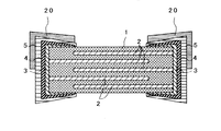
図1は、本発明をチップ型コンデンサーに適用した第1実施形態を示す断面図である。なお、以下の実施形態において、従来と同一箇所には同一符号を付してその説明を省略し、異なる箇所あるいは新たに付加された箇所にのみ異なる符号を用いて説明する。
Embodiments of the present invention will be described below with reference to the accompanying drawings.
[Chip-type electronic components]
FIG. 1 is a cross-sectional view showing a first embodiment in which the present invention is applied to a chip-type capacitor. In the following embodiments, the same reference numerals are used for the same parts as those in the prior art, and the description thereof is omitted, and only different parts or newly added parts are described using different reference numerals.
図1において、チップ型コンデンサーにおける外部電極外層5の側面上半部から上面にかけて、その外側部にはソルダーレジスト層20が形成され、外部電極外層5を覆っている。このソルダーレジスト層20は半田に対する非付着性の公知の樹脂材料が使用可能である。
In FIG. 1, a solder resist
この構造において、ソルダーレジスト層20の上面側は、誘電体1の上面周囲まで形成された状態を示しているが、ツームストーン防止の観点からは上面には設けなくてもよい。また、チップ型コンデンサーの実際の大きさは、前述のごとく長さ1.0mm、幅0.5mm、厚さ(高さ)0.5mmである。従って、ソルダーレジスト層20は、外部電極外層5の側面露出部の上半部である高さ0.25mmの位置より上の位置に形成されているが、ツームストーン防止効果と半田との付着性との兼合いで、この位置よりやや上側であっても、下側に位置していても良い。また、この構造は、チップ型電子部品の製造メーカーで製作された出来合のものに前記加工を加えるようにしても良いし、チップ型電子部品の製造の最終工程で前記加工を付加しても良く、いずれにおいてもその製作は簡単である。
In this structure, the upper surface side of the solder resist
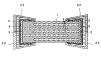
次に、図2はチップ型コンデンサーに適用した第2実施形態を示す断面図であり、本実施形態では、外部電極外層5の側面における上半部から上面にかけてその外側部をメッキレジスト層22で予め覆い、次いで外部電極外層5の下半部から下面にかけて電極メッキ層23を形成したものである。
Next, FIG. 2 is a cross-sectional view showing a second embodiment applied to a chip-type capacitor. In this embodiment, the outer side of the outer electrode
前記メッキレジスト層22は、第1実施形態のソロダーレジスト層20と同材質のものが使用可能である。メッキ方法としては、電解法、溶融金属浸漬法等をその材質や膜厚などに応じて選択できる。電極メッキ層23を構成する金属素材も、公知のものが使用可能である。
The plating resist
なお、以上の各実施形態では本発明のチップ型電子部品の一例としてチップ型コンデンサーを例示したが、各種抵抗素子、半導体など、チップ化可能な電子部品一般に適用可能である。 In each of the above embodiments, the chip type capacitor is exemplified as an example of the chip type electronic component of the present invention. However, the present invention is applicable to electronic components that can be made into chips, such as various resistance elements and semiconductors.
[チップ型電子部品の実装基板]
次に、以上のレジスト層を設けた前記チップ型コンデンサーを含むチップ型電子部品を基板上に実装する手順について、その実施形態を図3を用いて説明する。まず、基板10上に形成された基板電極11上には(a)に示すように、印刷などにより半田ペースト12が所定の厚みに塗布される。この塗布厚みは後述するチップ型電子部品の外部電極に対する接続面積が減少する分、従来に比べて薄く設計されていることは勿論である。
[Chip-type electronic component mounting board]
Next, a procedure for mounting a chip type electronic component including the chip type capacitor provided with the above resist layer on a substrate will be described with reference to FIG. First, as shown in (a), a
次いで(b)に示すように、両側部に前述する外部電極30を設け、その上半部を前記レジスト層20(22)で覆ったチップ型電子部品31が半田ペースト12上に供給される。この状態では設置位置の半田ペースト12は押しのけられた状態となり、かつチップ型電子部品31の荷重Wと半田ペースト12中のフラックス成分による粘着力F1によってチップ型電子部品31は両基板電極11上に位置決め状態に仮固定される。
Next, as shown in (b), the chip-type
その後、加熱することで半田ペースト12は溶融するが、このとき左右の半田ペースト12の溶融に僅かながらも時間差が生じた場合には、(c)に示すように、片側が溶融しても他方側が未だペースト状態にあることがある。この場合には、溶けた側の半田は、その濡れにより外部電極30の側面に沿って這い上がり、略直角三角形状断面に形成される。 但し、この這い上がり高さは、前記レジスト層20(22)の下縁までの高さであり、これ以上は該レジスト層20(22)によって阻止される。
After that, the
そして、この這い上がった半田による縦方向荷重Fyと横方向荷重Fxとの合力が界面張力となり、この界面張力方向に電子部品31を傾けようとする回転モーメントM1が生ずる。しかし、この回転モーメントM1は従来(図5参照)と比べて半減するため、この回転モーメントM1は未溶融側半田ペーストの粘着力F1と荷重Wの合力である回転抑止モーメントM2より小となることに加え、溶融側の底面に対する界面張力F1’の面積も相対的に増すことから、さらに回転力が減ぜられ、結果的には(d)に示すように、電子部品31は設置状態を保持されたまま、他方側の半田ペースト12が所定の時間遅れで溶融することで、完全に均衡が保たれる。
Then, the resultant force of the longitudinal load Fy and the lateral load Fx due to the scooped solder becomes an interfacial tension, and a rotational moment M1 is generated that tends to tilt the
その後は、冷却による半田の固化により両外側電極30を基板電極11に電気的に接続すると同時に、電子部品31の基板10に対する固定が完了するものとなる。
Thereafter, both
以上の実施形態では、ツームストーン現象を構造的な面から抑制できると同時に、半田の塗布量も削減できるため、高密度実装を歩留り良く、かつ経済的に達成できる。 In the above embodiment, the tombstone phenomenon can be suppressed from the structural aspect, and at the same time the amount of solder applied can be reduced, so that high-density mounting can be achieved with good yield and economically.
[チップ型電子部品実装基板が搭載された記録装置(電子機器)]
図1や図2に記載されたチップ型電子部品31が実装された実装基板は、各種電子機器に搭載して、各種制御実行に供される。電子機器の一例であるインクジェット式の記録装置は、被記録媒体を搬送する搬送部と、該搬送部によって搬送される被記録媒体に記録を実行する記録実行部と、前記搬送部および前記記録実行部の動作を制御する制御回路が形成されるチップ型電子部品実装基板とを備えている。このチップ型電子部品実装基板として上記実施の形態に係るチップ型電子部品の実装基板が使われている。これにより、インクジェット式の記録装置の各種動作における制御実行に際して、その安定性および信頼性を向上することができる。
[Recording device (electronic equipment) on which a chip-type electronic component mounting board is mounted]
The mounting substrate on which the chip-type
1 セラミック誘電体(電子部品本体)、 2 内部電極、 3 外部電極内層、 4 外部電極中間層、 5 外部電極外層、 10 基板、 11 基板電極、 12 半田ぺースト、 20,22 レジスト層、 23 金属メッキ層、 30 外部電極、 31 チップ型電子部品
DESCRIPTION OF
Claims (7)
前記外部電極の高さ方向上半部から上面周囲にかけてその外周がレジスト層で被覆されていることを特徴とするチップ型電子部品。 A chip-type electronic component comprising external electrodes formed on both sides of the electronic component body and conducting to the internal electrodes of the electronic component body, and a part of which extends around the upper and lower surfaces of the electronic component body; ,
A chip-type electronic component, wherein an outer periphery of the external electrode is covered with a resist layer from the upper half of the height direction to the periphery of the upper surface.
前記外部電極は多層構造に形成され、その最外層はその高さ方向上半部から上面周囲にかけてレジスト層で形成され、最外層の残りの部分は電極層で形成されていることを特徴とするチップ型電子部品。 A chip-type electronic component comprising external electrodes formed on both sides of the electronic component body and conducting to the internal electrodes of the electronic component body, and a part of which extends around the upper and lower surfaces of the electronic component body; ,
The external electrode is formed in a multilayer structure, the outermost layer is formed of a resist layer from the upper half of the height direction to the upper surface, and the remaining part of the outermost layer is formed of an electrode layer. Chip-type electronic components.
前記外部電極は多層構造に形成され、その最外層はその高さ方向上半部から上面周囲にかけてメッキレジスト層で形成され、最外層の残りの部分は前記メッキレジスト層が形成された状態でメッキされた電極メッキ層で形成されていることを特徴とするチップ型電子部品。 A chip-type electronic component comprising external electrodes formed on both sides of the electronic component body and conducting to the internal electrodes of the electronic component body, and a part of which extends around the upper and lower surfaces of the electronic component body; ,
The external electrode is formed in a multilayer structure, the outermost layer is formed of a plating resist layer from the upper half of the height direction to the periphery of the upper surface, and the remaining part of the outermost layer is plated with the plating resist layer formed. A chip-type electronic component, wherein the chip-type electronic component is formed of an electrode plating layer.
前記チップ型電子部品実装基板は請求項1から4のいずれか1項に記載されたチップ型電子部品の実装基板であることを特徴とする記録装置。 A chip on which a transport unit that transports a recording medium, a recording execution unit that performs recording on a recording medium transported by the transport unit, and a control circuit that controls operations of the transport unit and the recording execution unit are formed A recording apparatus comprising a mold-type electronic component mounting board,
5. The recording apparatus according to claim 1, wherein the chip-type electronic component mounting substrate is a chip-type electronic component mounting substrate according to claim 1.
Priority Applications (1)
| Application Number | Priority Date | Filing Date | Title |
|---|---|---|---|
| JP2006104232A JP2007281134A (en) | 2006-04-05 | 2006-04-05 | Chip-type electronic component, its mounting board, and its mounting method |
Applications Claiming Priority (1)
| Application Number | Priority Date | Filing Date | Title |
|---|---|---|---|
| JP2006104232A JP2007281134A (en) | 2006-04-05 | 2006-04-05 | Chip-type electronic component, its mounting board, and its mounting method |
Publications (1)
| Publication Number | Publication Date |
|---|---|
| JP2007281134A true JP2007281134A (en) | 2007-10-25 |
Family
ID=38682295
Family Applications (1)
| Application Number | Title | Priority Date | Filing Date |
|---|---|---|---|
| JP2006104232A Pending JP2007281134A (en) | 2006-04-05 | 2006-04-05 | Chip-type electronic component, its mounting board, and its mounting method |
Country Status (1)
| Country | Link |
|---|---|
| JP (1) | JP2007281134A (en) |
Cited By (21)
| Publication number | Priority date | Publication date | Assignee | Title |
|---|---|---|---|---|
| JP2010123865A (en) * | 2008-11-21 | 2010-06-03 | Murata Mfg Co Ltd | Ceramic electronic component and component built-in substrate |
| JP2012129272A (en) * | 2010-12-14 | 2012-07-05 | Citizen Electronics Co Ltd | Light emitting diode |
| WO2013161659A1 (en) * | 2012-04-25 | 2013-10-31 | 株式会社村田製作所 | Electronic component |
| US20140041913A1 (en) * | 2012-08-09 | 2014-02-13 | Tdk Corporation | Electronic circuit module component |
| JP2014036149A (en) * | 2012-08-09 | 2014-02-24 | Tdk Corp | Electronic component |
| JP2014053598A (en) * | 2012-08-09 | 2014-03-20 | Tdk Corp | Electronic component |
| JP2014086718A (en) * | 2012-10-26 | 2014-05-12 | Samsung Electro-Mechanics Co Ltd | Multilayered chip electronic component and board for mounting the same |
| JP2014187058A (en) * | 2013-01-14 | 2014-10-02 | Samsung Electro-Mechanics Co Ltd | Multilayer ceramic capacitor, mounting board for multilayer ceramic capacitor, and manufacturing method of multilayer ceramic capacitor |
| JP2015046422A (en) * | 2013-08-27 | 2015-03-12 | Tdk株式会社 | Ceramic electronic components |
| CN104465090A (en) * | 2013-09-25 | 2015-03-25 | 株式会社村田制作所 | Electronic component and method for manufacturing the same |
| CN104465078A (en) * | 2013-09-25 | 2015-03-25 | 株式会社村田制作所 | Electronic component and method for manufacturing the same |
| WO2016093153A1 (en) * | 2014-12-10 | 2016-06-16 | 東光株式会社 | Electronic component and method of manufacturing same |
| JP2017103321A (en) * | 2015-12-01 | 2017-06-08 | 太陽誘電株式会社 | Electronic component, manufacturing method thereof, and circuit board |
| JP2017228757A (en) * | 2016-06-21 | 2017-12-28 | サムソン エレクトロ−メカニックス カンパニーリミテッド. | Multilayer ceramic electronic component and mounting board thereof |
| JP2020035772A (en) * | 2018-08-27 | 2020-03-05 | 太陽誘電株式会社 | Ceramic electronic component, manufacturing method of ceramic electronic component and electronic component mounting circuit board |
| JP2023099426A (en) * | 2021-12-31 | 2023-07-13 | サムソン エレクトロ-メカニックス カンパニーリミテッド. | Multilayer electronic component |
| JP2023099430A (en) * | 2021-12-31 | 2023-07-13 | サムソン エレクトロ-メカニックス カンパニーリミテッド. | Multilayer electronic component |
| JP2023099433A (en) * | 2021-12-31 | 2023-07-13 | サムソン エレクトロ-メカニックス カンパニーリミテッド. | Multilayer electronic component |
| JP2023099428A (en) * | 2021-12-31 | 2023-07-13 | サムソン エレクトロ-メカニックス カンパニーリミテッド. | Multilayer electronic component |
| JP2023107724A (en) * | 2022-01-24 | 2023-08-03 | サムソン エレクトロ-メカニックス カンパニーリミテッド. | Multilayer electronic component |
| US12712127B2 (en) * | 2023-07-03 | 2026-08-18 | Samsung Electronics Co., Ltd. | Ceramic capacitor with prevention portions on end electrodes |
-
2006
- 2006-04-05 JP JP2006104232A patent/JP2007281134A/en active Pending
Cited By (33)
| Publication number | Priority date | Publication date | Assignee | Title |
|---|---|---|---|---|
| JP2010123865A (en) * | 2008-11-21 | 2010-06-03 | Murata Mfg Co Ltd | Ceramic electronic component and component built-in substrate |
| JP2012129272A (en) * | 2010-12-14 | 2012-07-05 | Citizen Electronics Co Ltd | Light emitting diode |
| WO2013161659A1 (en) * | 2012-04-25 | 2013-10-31 | 株式会社村田製作所 | Electronic component |
| US9320146B2 (en) * | 2012-08-09 | 2016-04-19 | Tdk Corporation | Electronic circuit module component |
| US20140041913A1 (en) * | 2012-08-09 | 2014-02-13 | Tdk Corporation | Electronic circuit module component |
| JP2014036149A (en) * | 2012-08-09 | 2014-02-24 | Tdk Corp | Electronic component |
| JP2014053598A (en) * | 2012-08-09 | 2014-03-20 | Tdk Corp | Electronic component |
| JP2014086718A (en) * | 2012-10-26 | 2014-05-12 | Samsung Electro-Mechanics Co Ltd | Multilayered chip electronic component and board for mounting the same |
| JP2015053503A (en) * | 2012-10-26 | 2015-03-19 | サムソン エレクトロ−メカニックス カンパニーリミテッド. | Multilayer chip electronic component and its mounting board |
| US9439301B2 (en) | 2012-10-26 | 2016-09-06 | Samsung Electro-Mechanics Co., Ltd. | Multilayered chip electronic component and board for mounting the same |
| JP2014187058A (en) * | 2013-01-14 | 2014-10-02 | Samsung Electro-Mechanics Co Ltd | Multilayer ceramic capacitor, mounting board for multilayer ceramic capacitor, and manufacturing method of multilayer ceramic capacitor |
| JP2015046422A (en) * | 2013-08-27 | 2015-03-12 | Tdk株式会社 | Ceramic electronic components |
| JP2015065284A (en) * | 2013-09-25 | 2015-04-09 | 株式会社村田製作所 | Electronic component and manufacturing method thereof |
| CN104465078A (en) * | 2013-09-25 | 2015-03-25 | 株式会社村田制作所 | Electronic component and method for manufacturing the same |
| CN104465090A (en) * | 2013-09-25 | 2015-03-25 | 株式会社村田制作所 | Electronic component and method for manufacturing the same |
| JP2015065283A (en) * | 2013-09-25 | 2015-04-09 | 株式会社村田製作所 | Electronic component and manufacturing method thereof |
| US9818511B2 (en) | 2013-09-25 | 2017-11-14 | Murata Manufacturing Co., Ltd. | Electronic component and method for manufacturing the same |
| US9818510B2 (en) | 2013-09-25 | 2017-11-14 | Murata Manufacturing Co., Ltd. | Electronic component and method for manufacturing the same |
| CN107004493B (en) * | 2014-12-10 | 2019-02-12 | 株式会社村田制作所 | Electronic component and method of manufacturing the same |
| WO2016093153A1 (en) * | 2014-12-10 | 2016-06-16 | 東光株式会社 | Electronic component and method of manufacturing same |
| CN107004493A (en) * | 2014-12-10 | 2017-08-01 | 株式会社村田制作所 | Electronic component and manufacturing method thereof |
| US10879005B2 (en) | 2014-12-10 | 2020-12-29 | Murata Manufacturing Co., Ltd. | Electronic component and method of manufacturing same |
| JP2017103321A (en) * | 2015-12-01 | 2017-06-08 | 太陽誘電株式会社 | Electronic component, manufacturing method thereof, and circuit board |
| JP2017228757A (en) * | 2016-06-21 | 2017-12-28 | サムソン エレクトロ−メカニックス カンパニーリミテッド. | Multilayer ceramic electronic component and mounting board thereof |
| JP2021153206A (en) * | 2016-06-21 | 2021-09-30 | サムソン エレクトロ−メカニックス カンパニーリミテッド. | Multilayer ceramic electronic components and their mounting boards |
| JP2020035772A (en) * | 2018-08-27 | 2020-03-05 | 太陽誘電株式会社 | Ceramic electronic component, manufacturing method of ceramic electronic component and electronic component mounting circuit board |
| JP7221616B2 (en) | 2018-08-27 | 2023-02-14 | 太陽誘電株式会社 | CERAMIC ELECTRONIC COMPONENT, METHOD FOR MANUFACTURING CERAMIC ELECTRONIC COMPONENT, AND ELECTRONIC COMPONENT MOUNTING CIRCUIT BOARD |
| JP2023099426A (en) * | 2021-12-31 | 2023-07-13 | サムソン エレクトロ-メカニックス カンパニーリミテッド. | Multilayer electronic component |
| JP2023099430A (en) * | 2021-12-31 | 2023-07-13 | サムソン エレクトロ-メカニックス カンパニーリミテッド. | Multilayer electronic component |
| JP2023099433A (en) * | 2021-12-31 | 2023-07-13 | サムソン エレクトロ-メカニックス カンパニーリミテッド. | Multilayer electronic component |
| JP2023099428A (en) * | 2021-12-31 | 2023-07-13 | サムソン エレクトロ-メカニックス カンパニーリミテッド. | Multilayer electronic component |
| JP2023107724A (en) * | 2022-01-24 | 2023-08-03 | サムソン エレクトロ-メカニックス カンパニーリミテッド. | Multilayer electronic component |
| US12712127B2 (en) * | 2023-07-03 | 2026-08-18 | Samsung Electronics Co., Ltd. | Ceramic capacitor with prevention portions on end electrodes |
Similar Documents
| Publication | Publication Date | Title |
|---|---|---|
| KR100680022B1 (en) | Substrate Reduction Structure and Substrate Reduction Method | |
| JP2014192476A (en) | Printed circuit board solder packaging method and solder packaging structure | |
| JP4200325B2 (en) | Solder bonding paste and solder bonding method | |
| JPH04192596A (en) | Mounting structure of electronic component | |
| JP2021125552A (en) | Printed circuit board and manufacturing method thereof, and printed wiring board | |
| JP2005203616A (en) | Chip component mounting structure and method therefor | |
| JP2009277777A (en) | Solder ball loading method and member for mounting electronic component | |
| JP4788754B2 (en) | Component built-in wiring board and method for manufacturing component built-in wiring board | |
| US8168525B2 (en) | Electronic part mounting board and method of mounting the same | |
| JP2006303173A (en) | Circuit board device and manufacturing method thereof | |
| US8300421B2 (en) | Electronic component and method of manufacturing electronic component | |
| JPS63273398A (en) | Reflow soldering method for printed substrate | |
| KR100764668B1 (en) | Flip chip connection board and its manufacturing method | |
| JP2007194665A (en) | Module manufacturing method | |
| JP2002026482A (en) | Mounting structure of electronic component | |
| TWM611216U (en) | Electronic circuit assembly | |
| JP2002016350A (en) | Soldering method | |
| JP5428572B2 (en) | Mounting structure for pin insertion parts | |
| JP2006319260A (en) | Chip resistor | |
| JP2013179192A (en) | Substrate and mounting method | |
| JP2011135111A (en) | Method for forming frame ground of printed circuit board | |
| JP4838277B2 (en) | Wiring board structure of electronic component mounting board and electronic component mounting structure | |
| JP2002374060A (en) | Electronic circuit board | |
| JPH11121915A (en) | Electronic component mounting method and electronic component mounting flux | |
| JP2008124363A (en) | Semiconductor device |