JP2007281181A - 半導体装置の製造方法 - Google Patents
半導体装置の製造方法 Download PDFInfo
- Publication number
- JP2007281181A JP2007281181A JP2006105442A JP2006105442A JP2007281181A JP 2007281181 A JP2007281181 A JP 2007281181A JP 2006105442 A JP2006105442 A JP 2006105442A JP 2006105442 A JP2006105442 A JP 2006105442A JP 2007281181 A JP2007281181 A JP 2007281181A
- Authority
- JP
- Japan
- Prior art keywords
- nitrogen
- layer
- semiconductor device
- silicon
- gate insulating
- Prior art date
- Legal status (The legal status is an assumption and is not a legal conclusion. Google has not performed a legal analysis and makes no representation as to the accuracy of the status listed.)
- Pending
Links
Images


Classifications
-
- H—ELECTRICITY
- H10—SEMICONDUCTOR DEVICES; ELECTRIC SOLID-STATE DEVICES NOT OTHERWISE PROVIDED FOR
- H10D—INORGANIC ELECTRIC SEMICONDUCTOR DEVICES
- H10D64/00—Electrodes of devices having potential barriers
- H10D64/01—Manufacture or treatment
- H10D64/013—Manufacture or treatment of electrodes having a conductor capacitively coupled to a semiconductor by an insulator
- H10D64/01302—Manufacture or treatment of electrodes having a conductor capacitively coupled to a semiconductor by an insulator the insulator being formed after the semiconductor body, the semiconductor being silicon
- H10D64/01332—Making the insulator
- H10D64/01336—Making the insulator on single crystalline silicon, e.g. chemical oxidation using a liquid
- H10D64/01344—Making the insulator on single crystalline silicon, e.g. chemical oxidation using a liquid in a nitrogen-containing ambient, e.g. N2O oxidation
-
- H—ELECTRICITY
- H10—SEMICONDUCTOR DEVICES; ELECTRIC SOLID-STATE DEVICES NOT OTHERWISE PROVIDED FOR
- H10P—GENERIC PROCESSES OR APPARATUS FOR THE MANUFACTURE OR TREATMENT OF DEVICES COVERED BY CLASS H10
- H10P14/00—Formation of materials, e.g. in the shape of layers or pillars
- H10P14/60—Formation of materials, e.g. in the shape of layers or pillars of insulating materials
- H10P14/63—Formation of materials, e.g. in the shape of layers or pillars of insulating materials characterised by the formation processes
- H10P14/6326—Deposition processes
- H10P14/6328—Deposition from the gas or vapour phase
- H10P14/6334—Deposition from the gas or vapour phase using decomposition or reaction of gaseous or vapour phase compounds, i.e. chemical vapour deposition
- H10P14/6336—Deposition from the gas or vapour phase using decomposition or reaction of gaseous or vapour phase compounds, i.e. chemical vapour deposition in the presence of a plasma [PECVD]
-
- H—ELECTRICITY
- H10—SEMICONDUCTOR DEVICES; ELECTRIC SOLID-STATE DEVICES NOT OTHERWISE PROVIDED FOR
- H10P—GENERIC PROCESSES OR APPARATUS FOR THE MANUFACTURE OR TREATMENT OF DEVICES COVERED BY CLASS H10
- H10P14/00—Formation of materials, e.g. in the shape of layers or pillars
- H10P14/60—Formation of materials, e.g. in the shape of layers or pillars of insulating materials
- H10P14/63—Formation of materials, e.g. in the shape of layers or pillars of insulating materials characterised by the formation processes
- H10P14/6302—Non-deposition formation processes
- H10P14/6304—Formation by oxidation, e.g. oxidation of the substrate
- H10P14/6306—Formation by oxidation, e.g. oxidation of the substrate of the semiconductor materials
- H10P14/6308—Formation by oxidation, e.g. oxidation of the substrate of the semiconductor materials of Group IV semiconductors
- H10P14/6309—Formation by oxidation, e.g. oxidation of the substrate of the semiconductor materials of Group IV semiconductors of silicon in uncombined form, i.e. pure silicon
-
- H—ELECTRICITY
- H10—SEMICONDUCTOR DEVICES; ELECTRIC SOLID-STATE DEVICES NOT OTHERWISE PROVIDED FOR
- H10P—GENERIC PROCESSES OR APPARATUS FOR THE MANUFACTURE OR TREATMENT OF DEVICES COVERED BY CLASS H10
- H10P14/00—Formation of materials, e.g. in the shape of layers or pillars
- H10P14/60—Formation of materials, e.g. in the shape of layers or pillars of insulating materials
- H10P14/63—Formation of materials, e.g. in the shape of layers or pillars of insulating materials characterised by the formation processes
- H10P14/6302—Non-deposition formation processes
- H10P14/6322—Formation by thermal treatments
-
- H—ELECTRICITY
- H10—SEMICONDUCTOR DEVICES; ELECTRIC SOLID-STATE DEVICES NOT OTHERWISE PROVIDED FOR
- H10P—GENERIC PROCESSES OR APPARATUS FOR THE MANUFACTURE OR TREATMENT OF DEVICES COVERED BY CLASS H10
- H10P14/00—Formation of materials, e.g. in the shape of layers or pillars
- H10P14/60—Formation of materials, e.g. in the shape of layers or pillars of insulating materials
- H10P14/63—Formation of materials, e.g. in the shape of layers or pillars of insulating materials characterised by the formation processes
- H10P14/6326—Deposition processes
- H10P14/6328—Deposition from the gas or vapour phase
- H10P14/6334—Deposition from the gas or vapour phase using decomposition or reaction of gaseous or vapour phase compounds, i.e. chemical vapour deposition
- H10P14/6339—Deposition from the gas or vapour phase using decomposition or reaction of gaseous or vapour phase compounds, i.e. chemical vapour deposition deposition by cyclic CVD, e.g. ALD, ALE or pulsed CVD
-
- H—ELECTRICITY
- H10—SEMICONDUCTOR DEVICES; ELECTRIC SOLID-STATE DEVICES NOT OTHERWISE PROVIDED FOR
- H10P—GENERIC PROCESSES OR APPARATUS FOR THE MANUFACTURE OR TREATMENT OF DEVICES COVERED BY CLASS H10
- H10P14/00—Formation of materials, e.g. in the shape of layers or pillars
- H10P14/60—Formation of materials, e.g. in the shape of layers or pillars of insulating materials
- H10P14/69—Inorganic materials
- H10P14/692—Inorganic materials composed of oxides, glassy oxides or oxide-based glasses
- H10P14/6921—Inorganic materials composed of oxides, glassy oxides or oxide-based glasses containing silicon
- H10P14/69215—Inorganic materials composed of oxides, glassy oxides or oxide-based glasses containing silicon the material being a silicon oxide, e.g. SiO2
-
- H—ELECTRICITY
- H10—SEMICONDUCTOR DEVICES; ELECTRIC SOLID-STATE DEVICES NOT OTHERWISE PROVIDED FOR
- H10P—GENERIC PROCESSES OR APPARATUS FOR THE MANUFACTURE OR TREATMENT OF DEVICES COVERED BY CLASS H10
- H10P14/00—Formation of materials, e.g. in the shape of layers or pillars
- H10P14/60—Formation of materials, e.g. in the shape of layers or pillars of insulating materials
- H10P14/69—Inorganic materials
- H10P14/692—Inorganic materials composed of oxides, glassy oxides or oxide-based glasses
- H10P14/6921—Inorganic materials composed of oxides, glassy oxides or oxide-based glasses containing silicon
- H10P14/6922—Inorganic materials composed of oxides, glassy oxides or oxide-based glasses containing silicon the material containing Si, O and at least one of H, N, C, F or other non-metal elements, e.g. SiOC, SiOC:H or SiONC
- H10P14/6927—Inorganic materials composed of oxides, glassy oxides or oxide-based glasses containing silicon the material containing Si, O and at least one of H, N, C, F or other non-metal elements, e.g. SiOC, SiOC:H or SiONC the material being a silicon oxynitride, e.g. SiON or SiON:H
-
- H—ELECTRICITY
- H10—SEMICONDUCTOR DEVICES; ELECTRIC SOLID-STATE DEVICES NOT OTHERWISE PROVIDED FOR
- H10P—GENERIC PROCESSES OR APPARATUS FOR THE MANUFACTURE OR TREATMENT OF DEVICES COVERED BY CLASS H10
- H10P14/00—Formation of materials, e.g. in the shape of layers or pillars
- H10P14/60—Formation of materials, e.g. in the shape of layers or pillars of insulating materials
- H10P14/69—Inorganic materials
- H10P14/694—Inorganic materials composed of nitrides
- H10P14/6943—Inorganic materials composed of nitrides containing silicon
- H10P14/69433—Inorganic materials composed of nitrides containing silicon the material being a silicon nitride not containing oxygen, e.g. SixNy or SixByNz
Landscapes
- Insulated Gate Type Field-Effect Transistor (AREA)
- Formation Of Insulating Films (AREA)
- Chemical Vapour Deposition (AREA)
Abstract
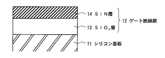
【解決手段】シリコン基板11上にSiO2層13を形成する工程と、SiO2層13上にALD法を用いてSiN膜の化学量論的組成よりも窒素が少ないSiN層14を形成する工程と、SiN層14を500℃未満の基板温度でプラズマ窒化処理する工程とを有する。
【選択図】図1
Description
SiN膜の化学量論的組成よりも窒素が少ない窒素含有シリコン膜を形成する工程と、
前記窒素含有シリコン膜を窒化する工程とを有することを特徴とする。
12:ゲート絶縁膜
13:SiO2層
14:SiN層
21:シリコン単原子層
21a:シリコン
Claims (8)
- シリコン基板上に窒素含有ゲート絶縁膜を形成する、半導体装置の製造方法であって、
SiN膜の化学量論的組成よりも窒素が少ない窒素含有シリコン膜を形成する工程と、
前記窒素含有シリコン膜を窒化する工程とを有することを特徴とする半導体装置の製造方法。 - 前記窒化工程は、500℃未満の基板温度を採用するプラズマ窒化法で行う、請求項1に記載の半導体装置の製造方法。
- 前記窒化工程は、窒素雰囲気下で800℃以下の基板温度で行う、請求項1に記載の半導体装置の製造方法。
- 前記窒素含有シリコン膜を形成する工程に先立って、シリコン基板上にシリコン酸化膜を形成する工程を更に有する、請求項1〜3の何れか一に記載の半導体装置の製造方法。
- 前記窒素含有シリコン膜を形成する工程は、シリコン単原子層を堆積する工程と、該シリコン単原子層を窒化する工程とを繰り返し行う、請求項1〜4の何れか一に記載の半導体装置の製造方法。
- 前記シリコン単原子層を窒化する工程は、500℃以上の基板温度を採用するプラズマ窒化法で行う、請求項5に記載の半導体装置の製造方法。
- 前記窒素含有シリコン膜を窒化する工程では、シリコン基板に近い側の表面部分の窒化濃度が、シリコン基板から遠い側の表面部分の窒化濃度よりも低くなるように窒化する、請求項1〜6の何れか一に記載の半導体装置の製造方法。
- 前記窒素含有シリコン膜がSiON膜である、請求項1〜4の何れか一に記載の半導体装置の製造方法。
Priority Applications (2)
| Application Number | Priority Date | Filing Date | Title |
|---|---|---|---|
| JP2006105442A JP2007281181A (ja) | 2006-04-06 | 2006-04-06 | 半導体装置の製造方法 |
| US11/697,050 US8105959B2 (en) | 2006-04-06 | 2007-04-05 | Method for manufacturing a semiconductor device having a nitrogen-containing gate insulating film |
Applications Claiming Priority (1)
| Application Number | Priority Date | Filing Date | Title |
|---|---|---|---|
| JP2006105442A JP2007281181A (ja) | 2006-04-06 | 2006-04-06 | 半導体装置の製造方法 |
Publications (1)
| Publication Number | Publication Date |
|---|---|
| JP2007281181A true JP2007281181A (ja) | 2007-10-25 |
Family
ID=38575885
Family Applications (1)
| Application Number | Title | Priority Date | Filing Date |
|---|---|---|---|
| JP2006105442A Pending JP2007281181A (ja) | 2006-04-06 | 2006-04-06 | 半導体装置の製造方法 |
Country Status (2)
| Country | Link |
|---|---|
| US (1) | US8105959B2 (ja) |
| JP (1) | JP2007281181A (ja) |
Cited By (22)
| Publication number | Priority date | Publication date | Assignee | Title |
|---|---|---|---|---|
| JP2012216631A (ja) * | 2011-03-31 | 2012-11-08 | Tokyo Electron Ltd | プラズマ窒化処理方法 |
| US8420482B2 (en) | 2008-09-05 | 2013-04-16 | Samsung Electronics Co., Ltd. | Nonvolatile memory device and method of forming the same |
| JP2014013928A (ja) * | 2008-11-26 | 2014-01-23 | Hitachi Kokusai Electric Inc | 半導体装置の製造方法及び基板処理装置 |
| US9312123B2 (en) | 2008-11-26 | 2016-04-12 | Hitachi Kokusai Electric Inc. | Method of manufacturing semiconductor device and substrate processing apparatus |
| US20170103885A1 (en) | 2014-06-25 | 2017-04-13 | Hitachi Kokusai Electric Inc. | Method for manufacturing semiconductor device, substrate-processing apparatus, and recording medium |
| US9741555B2 (en) | 2015-01-14 | 2017-08-22 | Hitachi Kokusai Electric Inc. | Method of manufacturing semiconductor device, substrate processing apparatus, and recording medium |
| WO2018089314A1 (en) * | 2016-11-11 | 2018-05-17 | Lam Research Corporation | Method for reducing the wet etch rate of a sin film without damaging the underlying substrate |
| US10074543B2 (en) | 2016-08-31 | 2018-09-11 | Lam Research Corporation | High dry etch rate materials for semiconductor patterning applications |
| US10134579B2 (en) | 2016-11-14 | 2018-11-20 | Lam Research Corporation | Method for high modulus ALD SiO2 spacer |
| US10157736B2 (en) | 2016-05-06 | 2018-12-18 | Lam Research Corporation | Methods of encapsulation |
| US10269559B2 (en) | 2017-09-13 | 2019-04-23 | Lam Research Corporation | Dielectric gapfill of high aspect ratio features utilizing a sacrificial etch cap layer |
| US10629435B2 (en) | 2016-07-29 | 2020-04-21 | Lam Research Corporation | Doped ALD films for semiconductor patterning applications |
| US10804099B2 (en) | 2014-11-24 | 2020-10-13 | Lam Research Corporation | Selective inhibition in atomic layer deposition of silicon-containing films |
| US10825680B2 (en) | 2015-12-18 | 2020-11-03 | Lam Research Corporation | Directional deposition on patterned structures |
| US10832908B2 (en) | 2016-11-11 | 2020-11-10 | Lam Research Corporation | Self-aligned multi-patterning process flow with ALD gapfill spacer mask |
| US11404275B2 (en) | 2018-03-02 | 2022-08-02 | Lam Research Corporation | Selective deposition using hydrolysis |
| US11832533B2 (en) | 2018-08-24 | 2023-11-28 | Lam Research Corporation | Conformal damage-free encapsulation of chalcogenide materials |
| US12157945B2 (en) | 2019-08-06 | 2024-12-03 | Lam Research Corporation | Thermal atomic layer deposition of silicon-containing films |
| US12237175B2 (en) | 2019-06-04 | 2025-02-25 | Lam Research Corporation | Polymerization protective liner for reactive ion etch in patterning |
| US12412742B2 (en) | 2020-07-28 | 2025-09-09 | Lam Research Corporation | Impurity reduction in silicon-containing films |
| US12473633B2 (en) | 2021-07-09 | 2025-11-18 | Lam Research Corporation | Plasma enhanced atomic layer deposition of silicon-containing films |
| US12598930B2 (en) | 2020-07-23 | 2026-04-07 | Lam Research Corporation | Conformal thermal CVD with controlled film properties and high deposition rate |
Families Citing this family (5)
| Publication number | Priority date | Publication date | Assignee | Title |
|---|---|---|---|---|
| US7910497B2 (en) * | 2007-07-30 | 2011-03-22 | Applied Materials, Inc. | Method of forming dielectric layers on a substrate and apparatus therefor |
| US7704884B2 (en) * | 2008-04-11 | 2010-04-27 | Micron Technology, Inc. | Semiconductor processing methods |
| KR101039142B1 (ko) * | 2008-12-23 | 2011-06-03 | 주식회사 하이닉스반도체 | 리세스 채널을 갖는 반도체 소자의 제조방법 |
| US9006064B2 (en) | 2013-03-11 | 2015-04-14 | International Business Machines Corporation | Multi-plasma nitridation process for a gate dielectric |
| JP6369680B2 (ja) * | 2014-05-30 | 2018-08-08 | パナソニックIpマネジメント株式会社 | 太陽電池 |
Citations (9)
| Publication number | Priority date | Publication date | Assignee | Title |
|---|---|---|---|---|
| JPS5984460A (ja) * | 1982-11-04 | 1984-05-16 | Nec Corp | 半導体装置用キヤパシタの製造方法 |
| JP2001237243A (ja) * | 1999-12-23 | 2001-08-31 | Asm America Inc | インシチュ誘電体スタックの製造方法及びそのプロセス |
| JP2002203961A (ja) * | 2000-12-28 | 2002-07-19 | Sony Corp | ゲート絶縁膜の形成方法 |
| JP2003218106A (ja) * | 2002-01-23 | 2003-07-31 | Hitachi Kokusai Electric Inc | 半導体装置の製造方法 |
| JP2004022902A (ja) * | 2002-06-18 | 2004-01-22 | Fujitsu Ltd | 半導体装置の製造方法 |
| JP2005079308A (ja) * | 2003-08-29 | 2005-03-24 | Semiconductor Leading Edge Technologies Inc | 半導体装置の製造方法 |
| JP2006073758A (ja) * | 2004-09-01 | 2006-03-16 | Hitachi Kokusai Electric Inc | 半導体装置の製造方法 |
| JP2006108493A (ja) * | 2004-10-07 | 2006-04-20 | Oki Electric Ind Co Ltd | 半導体装置の製造方法 |
| JP2007194239A (ja) * | 2006-01-17 | 2007-08-02 | Fujitsu Ltd | 半導体装置の製造方法 |
Family Cites Families (10)
| Publication number | Priority date | Publication date | Assignee | Title |
|---|---|---|---|---|
| US4398339A (en) * | 1977-04-15 | 1983-08-16 | Supertex, Inc. | Fabrication method for high power MOS device |
| US6566281B1 (en) * | 1997-10-15 | 2003-05-20 | International Business Machines Corporation | Nitrogen-rich barrier layer and structures formed |
| US6309932B1 (en) * | 1999-01-14 | 2001-10-30 | Agere Systems Guardian Corp | Process for forming a plasma nitride film suitable for gate dielectric application in sub-0.25 μm technologies |
| JP3538081B2 (ja) * | 1999-08-24 | 2004-06-14 | 松下電器産業株式会社 | 半導体装置の製造方法 |
| US20030059535A1 (en) * | 2001-09-25 | 2003-03-27 | Lee Luo | Cycling deposition of low temperature films in a cold wall single wafer process chamber |
| US6638879B2 (en) * | 2001-12-06 | 2003-10-28 | Macronix International Co., Ltd. | Method for forming nitride spacer by using atomic layer deposition |
| KR100469126B1 (ko) * | 2002-06-05 | 2005-01-29 | 삼성전자주식회사 | 수소 함유량이 적은 박막 형성방법 |
| US6821868B2 (en) * | 2002-12-27 | 2004-11-23 | Taiwan Semiconductor Manufacturing Co., Ltd. | Method of forming nitrogen enriched gate dielectric with low effective oxide thickness |
| US7545001B2 (en) * | 2003-11-25 | 2009-06-09 | Taiwan Semiconductor Manufacturing Company | Semiconductor device having high drive current and method of manufacture therefor |
| US7429538B2 (en) * | 2005-06-27 | 2008-09-30 | Applied Materials, Inc. | Manufacturing method for two-step post nitridation annealing of plasma nitrided gate dielectric |
-
2006
- 2006-04-06 JP JP2006105442A patent/JP2007281181A/ja active Pending
-
2007
- 2007-04-05 US US11/697,050 patent/US8105959B2/en not_active Expired - Fee Related
Patent Citations (9)
| Publication number | Priority date | Publication date | Assignee | Title |
|---|---|---|---|---|
| JPS5984460A (ja) * | 1982-11-04 | 1984-05-16 | Nec Corp | 半導体装置用キヤパシタの製造方法 |
| JP2001237243A (ja) * | 1999-12-23 | 2001-08-31 | Asm America Inc | インシチュ誘電体スタックの製造方法及びそのプロセス |
| JP2002203961A (ja) * | 2000-12-28 | 2002-07-19 | Sony Corp | ゲート絶縁膜の形成方法 |
| JP2003218106A (ja) * | 2002-01-23 | 2003-07-31 | Hitachi Kokusai Electric Inc | 半導体装置の製造方法 |
| JP2004022902A (ja) * | 2002-06-18 | 2004-01-22 | Fujitsu Ltd | 半導体装置の製造方法 |
| JP2005079308A (ja) * | 2003-08-29 | 2005-03-24 | Semiconductor Leading Edge Technologies Inc | 半導体装置の製造方法 |
| JP2006073758A (ja) * | 2004-09-01 | 2006-03-16 | Hitachi Kokusai Electric Inc | 半導体装置の製造方法 |
| JP2006108493A (ja) * | 2004-10-07 | 2006-04-20 | Oki Electric Ind Co Ltd | 半導体装置の製造方法 |
| JP2007194239A (ja) * | 2006-01-17 | 2007-08-02 | Fujitsu Ltd | 半導体装置の製造方法 |
Cited By (46)
| Publication number | Priority date | Publication date | Assignee | Title |
|---|---|---|---|---|
| USRE46389E1 (en) | 2008-09-05 | 2017-05-02 | Samsung Electronics Co., Ltd. | Nonvolatile memory device and method of forming the same |
| US8420482B2 (en) | 2008-09-05 | 2013-04-16 | Samsung Electronics Co., Ltd. | Nonvolatile memory device and method of forming the same |
| US9384972B2 (en) | 2008-11-26 | 2016-07-05 | Hitachi Kokusai Electric Inc. | Method of manufacturing semiconductor device by forming a film on a substrate |
| US9385013B2 (en) | 2008-11-26 | 2016-07-05 | Hitachi Kokusai Electric Inc. | Method and apparatus of manufacturing a semiconductor device by forming a film on a substrate |
| US9312123B2 (en) | 2008-11-26 | 2016-04-12 | Hitachi Kokusai Electric Inc. | Method of manufacturing semiconductor device and substrate processing apparatus |
| US9318316B2 (en) | 2008-11-26 | 2016-04-19 | Hitachi Kokusai Electric Inc. | Method of manufacturing semiconductor device, method of processing substrate and substrate processing apparatus for forming thin film containing at least two different elements |
| US9330904B2 (en) | 2008-11-26 | 2016-05-03 | Hitachi Kokusai Electric Inc. | Method of manufacturing semiconductor device and substrate processing apparatus |
| US9384967B2 (en) | 2008-11-26 | 2016-07-05 | Hitachi Kokusai Electric Inc. | Method of manufacturing a semiconductor device by forming a film on a substrate |
| US9384968B2 (en) | 2008-11-26 | 2016-07-05 | Hitachi Kokusai Electric Inc. | Method of manufacturing a semiconductor device by forming a film on a substrate |
| US9384971B2 (en) | 2008-11-26 | 2016-07-05 | Hitachi Kokusai Electric Inc. | Method of manufacturing semiconductor device by forming a film on a substrate |
| US9384970B2 (en) | 2008-11-26 | 2016-07-05 | Hitachi Kokusai Electric Inc. | Method of manufacturing semiconductor device by forming a film on a substrate |
| US9384969B2 (en) | 2008-11-26 | 2016-07-05 | Hitachi Kokusai Electric Inc. | Method of manufacturing semiconductor device by forming a film on a substrate |
| US9384966B2 (en) | 2008-11-26 | 2016-07-05 | Hitachi Kokusai Electric Inc. | Method of manufacturing a semiconductor device by forming a film on a substrate |
| US9487861B2 (en) | 2008-11-26 | 2016-11-08 | Hitachi Kokusai Electric Inc. | Substrate processing apparatus capable of forming films including at least two different elements |
| US10026607B2 (en) | 2008-11-26 | 2018-07-17 | Hitachi Kokusai Electric, Inc. | Substrate processing apparatus for forming film including at least two different elements |
| US9443720B2 (en) | 2008-11-26 | 2016-09-13 | Hitachi Kokusai Electric Inc. | Method of manufacturing semiconductor device for forming film including at least two different elements |
| JP2015133506A (ja) * | 2008-11-26 | 2015-07-23 | 株式会社日立国際電気 | 半導体装置の製造方法及び基板処理装置 |
| US9478417B2 (en) | 2008-11-26 | 2016-10-25 | Hitachi Kokusai Electric Inc. | Method of manufacturing semiconductor device for forming film including at least two different elements |
| US9443719B2 (en) | 2008-11-26 | 2016-09-13 | Hitachi Kokusai Electric Inc. | Method of manufacturing semiconductor device for forming film including at least two different elements |
| JP2014013928A (ja) * | 2008-11-26 | 2014-01-23 | Hitachi Kokusai Electric Inc | 半導体装置の製造方法及び基板処理装置 |
| JP2012216631A (ja) * | 2011-03-31 | 2012-11-08 | Tokyo Electron Ltd | プラズマ窒化処理方法 |
| US20170103885A1 (en) | 2014-06-25 | 2017-04-13 | Hitachi Kokusai Electric Inc. | Method for manufacturing semiconductor device, substrate-processing apparatus, and recording medium |
| US10229829B2 (en) | 2014-06-25 | 2019-03-12 | Kokusai Electric Corporation | Method for manufacturing semiconductor device, substrate-processing apparatus, and recording medium |
| US10497561B2 (en) | 2014-06-25 | 2019-12-03 | Kokusai Electric Corporation | Method for manufacturing semiconductor device, substrate-processing apparatus, and recording medium |
| US10163625B2 (en) | 2014-06-25 | 2018-12-25 | Hitachi Kokusai Electric Inc. | Method for manufacturing semiconductor device, substrate-processing apparatus, and recording medium |
| US10804099B2 (en) | 2014-11-24 | 2020-10-13 | Lam Research Corporation | Selective inhibition in atomic layer deposition of silicon-containing films |
| US9741555B2 (en) | 2015-01-14 | 2017-08-22 | Hitachi Kokusai Electric Inc. | Method of manufacturing semiconductor device, substrate processing apparatus, and recording medium |
| US10825680B2 (en) | 2015-12-18 | 2020-11-03 | Lam Research Corporation | Directional deposition on patterned structures |
| US10157736B2 (en) | 2016-05-06 | 2018-12-18 | Lam Research Corporation | Methods of encapsulation |
| US10763107B2 (en) | 2016-05-06 | 2020-09-01 | Lam Research Corporation | Methods of encapsulation |
| US10566186B2 (en) | 2016-05-06 | 2020-02-18 | Lam Research Corporation | Methods of encapsulation |
| US10629435B2 (en) | 2016-07-29 | 2020-04-21 | Lam Research Corporation | Doped ALD films for semiconductor patterning applications |
| US10074543B2 (en) | 2016-08-31 | 2018-09-11 | Lam Research Corporation | High dry etch rate materials for semiconductor patterning applications |
| US10832908B2 (en) | 2016-11-11 | 2020-11-10 | Lam Research Corporation | Self-aligned multi-patterning process flow with ALD gapfill spacer mask |
| WO2018089314A1 (en) * | 2016-11-11 | 2018-05-17 | Lam Research Corporation | Method for reducing the wet etch rate of a sin film without damaging the underlying substrate |
| US10454029B2 (en) | 2016-11-11 | 2019-10-22 | Lam Research Corporation | Method for reducing the wet etch rate of a sin film without damaging the underlying substrate |
| US10134579B2 (en) | 2016-11-14 | 2018-11-20 | Lam Research Corporation | Method for high modulus ALD SiO2 spacer |
| US10658172B2 (en) | 2017-09-13 | 2020-05-19 | Lam Research Corporation | Dielectric gapfill of high aspect ratio features utilizing a sacrificial etch cap layer |
| US10269559B2 (en) | 2017-09-13 | 2019-04-23 | Lam Research Corporation | Dielectric gapfill of high aspect ratio features utilizing a sacrificial etch cap layer |
| US11404275B2 (en) | 2018-03-02 | 2022-08-02 | Lam Research Corporation | Selective deposition using hydrolysis |
| US11832533B2 (en) | 2018-08-24 | 2023-11-28 | Lam Research Corporation | Conformal damage-free encapsulation of chalcogenide materials |
| US12237175B2 (en) | 2019-06-04 | 2025-02-25 | Lam Research Corporation | Polymerization protective liner for reactive ion etch in patterning |
| US12157945B2 (en) | 2019-08-06 | 2024-12-03 | Lam Research Corporation | Thermal atomic layer deposition of silicon-containing films |
| US12598930B2 (en) | 2020-07-23 | 2026-04-07 | Lam Research Corporation | Conformal thermal CVD with controlled film properties and high deposition rate |
| US12412742B2 (en) | 2020-07-28 | 2025-09-09 | Lam Research Corporation | Impurity reduction in silicon-containing films |
| US12473633B2 (en) | 2021-07-09 | 2025-11-18 | Lam Research Corporation | Plasma enhanced atomic layer deposition of silicon-containing films |
Also Published As
| Publication number | Publication date |
|---|---|
| US8105959B2 (en) | 2012-01-31 |
| US20070238316A1 (en) | 2007-10-11 |
Similar Documents
| Publication | Publication Date | Title |
|---|---|---|
| JP2007281181A (ja) | 半導体装置の製造方法 | |
| US7994070B1 (en) | Low-temperature dielectric film formation by chemical vapor deposition | |
| KR100640638B1 (ko) | 원자층 증착법에 의한 고유전막 형성 방법 및 고유전막을 갖는 반도체소자의 제조 방법 | |
| KR101340098B1 (ko) | 반도체 장치의 제조 방법 | |
| US7704858B2 (en) | Methods of forming nickel silicide layers with low carbon content | |
| US7768036B2 (en) | Integrated circuitry | |
| US7482234B2 (en) | Method of fabricating a metal oxynitride thin film that includes a first annealing of a metal oxide film in a nitrogen-containing atmosphere to form a metal oxynitride film and a second annealing of the metal oxynitride film in an oxidizing atmosphere | |
| KR20150090848A (ko) | 반도체 장치의 제조 방법 | |
| US7402472B2 (en) | Method of making a nitrided gate dielectric | |
| WO2004107451A1 (ja) | Mis型電界効果トランジスタを備える半導体装置及びその製造方法並びに金属酸化膜の形成方法 | |
| US7592234B2 (en) | Method for forming a nitrogen-containing gate insulating film | |
| KR100788361B1 (ko) | 모스펫 소자의 형성 방법 | |
| US20060273411A1 (en) | In-situ nitridation of high-k dielectrics | |
| CN105336784A (zh) | 半导体器件及其制造方法 | |
| JP2008235397A (ja) | 半導体装置の製造方法 | |
| JP4719422B2 (ja) | 半導体装置の製造方法 | |
| JP2006066706A (ja) | 高誘電体膜、この高誘電体膜を用いた電界効果トランジスタおよび半導体集積回路装置ならびに高誘電体膜の製造方法 | |
| JP5141321B2 (ja) | 半導体装置の製造方法 | |
| KR20080062743A (ko) | 반도체소자 및 그 제조방법 | |
| JP5325759B2 (ja) | 半導体装置の製造方法 | |
| JP2008041825A (ja) | 半導体装置の製造方法 | |
| KR100680970B1 (ko) | 반도체 소자의 게이트 형성방법 | |
| KR100745073B1 (ko) | 하프늄니오븀옥사이드(HfNbO) 게이트절연막을 갖는반도체소자 및 그 제조방법 | |
| JP2005285805A (ja) | 半導体装置の製造方法 | |
| KR100650758B1 (ko) | 반도체 소자의 게이트 형성방법 |
Legal Events
| Date | Code | Title | Description |
|---|---|---|---|
| A621 | Written request for application examination |
Free format text: JAPANESE INTERMEDIATE CODE: A621 Effective date: 20090310 |
|
| A977 | Report on retrieval |
Free format text: JAPANESE INTERMEDIATE CODE: A971007 Effective date: 20090910 |
|
| RD01 | Notification of change of attorney |
Free format text: JAPANESE INTERMEDIATE CODE: A7421 Effective date: 20100205 |
|
| A131 | Notification of reasons for refusal |
Free format text: JAPANESE INTERMEDIATE CODE: A131 Effective date: 20111011 |
|
| A521 | Request for written amendment filed |
Free format text: JAPANESE INTERMEDIATE CODE: A523 Effective date: 20111207 |
|
| A02 | Decision of refusal |
Free format text: JAPANESE INTERMEDIATE CODE: A02 Effective date: 20111227 |