JP2007281187A - Electronic apparatus - Google Patents
Electronic apparatus Download PDFInfo
- Publication number
- JP2007281187A JP2007281187A JP2006105532A JP2006105532A JP2007281187A JP 2007281187 A JP2007281187 A JP 2007281187A JP 2006105532 A JP2006105532 A JP 2006105532A JP 2006105532 A JP2006105532 A JP 2006105532A JP 2007281187 A JP2007281187 A JP 2007281187A
- Authority
- JP
- Japan
- Prior art keywords
- lead
- electrode terminal
- electronic component
- electronic device
- electrolytic capacitor
- Prior art date
- Legal status (The legal status is an assumption and is not a legal conclusion. Google has not performed a legal analysis and makes no representation as to the accuracy of the status listed.)
- Pending
Links
- 239000003990 capacitor Substances 0.000 claims abstract description 60
- 238000003466 welding Methods 0.000 claims description 15
- 230000033228 biological regulation Effects 0.000 claims description 6
- 230000001105 regulatory effect Effects 0.000 claims description 2
- RYGMFSIKBFXOCR-UHFFFAOYSA-N Copper Chemical compound [Cu] RYGMFSIKBFXOCR-UHFFFAOYSA-N 0.000 abstract description 52
- 229910052802 copper Inorganic materials 0.000 abstract description 52
- 239000010949 copper Substances 0.000 abstract description 52
- 239000011347 resin Substances 0.000 abstract description 14
- 229920005989 resin Polymers 0.000 abstract description 14
- 230000003534 oscillatory effect Effects 0.000 abstract 1
- 238000005452 bending Methods 0.000 description 5
- 238000005476 soldering Methods 0.000 description 4
- 230000000694 effects Effects 0.000 description 3
- 125000006850 spacer group Chemical group 0.000 description 3
- 235000014676 Phragmites communis Nutrition 0.000 description 2
- 230000004308 accommodation Effects 0.000 description 2
- 239000012141 concentrate Substances 0.000 description 2
- 230000006378 damage Effects 0.000 description 2
- 238000006073 displacement reaction Methods 0.000 description 2
- 229910052782 aluminium Inorganic materials 0.000 description 1
- XAGFODPZIPBFFR-UHFFFAOYSA-N aluminium Chemical compound [Al] XAGFODPZIPBFFR-UHFFFAOYSA-N 0.000 description 1
- 239000000919 ceramic Substances 0.000 description 1
- 230000007423 decrease Effects 0.000 description 1
- 230000003247 decreasing effect Effects 0.000 description 1
- 239000011810 insulating material Substances 0.000 description 1
- 239000000463 material Substances 0.000 description 1
- 229910052751 metal Inorganic materials 0.000 description 1
- 239000002184 metal Substances 0.000 description 1
- 238000000465 moulding Methods 0.000 description 1
Images

Landscapes
- Mounting Components In General For Electric Apparatus (AREA)
Abstract
Description
本発明は、リードが電極端子と電気的に接続されるように固着された電子部品を備えた電子機器に関する。 The present invention relates to an electronic device including an electronic component fixed so that a lead is electrically connected to an electrode terminal.
従来、電子機器において、コンデンサ(電解コンデンサ)を収容部に収容するとともに、コンデンサのリードをL字状に屈曲させた状態で電極端子と電気的に接続している場合がある。この場合、収容部とコンデンサとにそれぞれ寸法公差が存在するため、電子部品を収容部に収容すると、コンデンサと収容部との間には隙間(ガタ)が存在する。そこで、リードと電極端子とを接続する際には、リードと電極との接続位置がずれることのないように、作業者が電子部品を保持しつつ接続作業を行うか、若しくは、コンデンサと収容部との間に存在する隙間を埋めるためのスペーサを配置していた。 2. Description of the Related Art Conventionally, in an electronic device, a capacitor (electrolytic capacitor) may be housed in a housing portion and electrically connected to an electrode terminal with a capacitor lead bent in an L shape. In this case, since there is a dimensional tolerance between the housing part and the capacitor, when the electronic component is housed in the housing part, there is a gap (backlash) between the capacitor and the housing part. Therefore, when connecting the lead and the electrode terminal, the operator performs the connection work while holding the electronic component so that the connection position of the lead and the electrode is not shifted, or the capacitor and the housing portion. A spacer for filling a gap existing between the two is disposed.
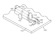
また、従来、作業者が保持しなくとも、電子部品を電極と電気的に接続する際に電子部品を保持できる電子機器が提案されている(特許文献1参照。)。特許文献1に記載の電子機器100では、図4に示すように、電子部品101の幅方向において当接する一対の幅方向ガイド102を端子基板103に一体成形している。そして、電子部品101のリード104を電極端子105と電気的に接続する際に一対の幅方向ガイド102に電子部品101を嵌着させることで、電子部品101の位置を保持している。さらに、特許文献1に記載の電子機器では、図4に示すように一対の長手方向嵌着片106の上端部に形成されている抜止め突起107によって電子部品101が端子基板103から抜けることを防止している。
ところが、従来の電子機器では、コンデンサの寸法公差と収容部の寸法公差との影響を受けるため、リードと電極端子との接続位置が予め設定していた位置からずれることがあった。そして、リードがL字状に屈曲された構成では、接続位置のずれが大きいとリードを電極端子と電気的に接続した状態でリードに引っ張り力を加える状態となる場合がある。また、スペーサを隙間に配置して対応したとしても、スペーサを配置することを作業者が忘れてしまい、隙間が存在したままの状態になる場合もある。この状態で、電子機器を振動状態で使用すると、リードの基端部に応力が集中してコンデンサの耐久性が低下する。 However, in the conventional electronic device, since the dimensional tolerance of the capacitor and the dimensional tolerance of the housing portion are affected, the connection position between the lead and the electrode terminal may deviate from the preset position. In the configuration in which the lead is bent in an L shape, there is a case where a tensile force is applied to the lead while the lead is electrically connected to the electrode terminal when the displacement of the connection position is large. Further, even if the spacer is arranged in the gap, the operator may forget to arrange the spacer, and the gap may remain. In this state, when the electronic device is used in a vibration state, stress concentrates on the base end portion of the lead, and the durability of the capacitor is lowered.
特許文献1に記載の電子機器100においては、電子部品101における寸法T1の公差と、一対の長手方向嵌着片106間の寸法T2の公差の影響によって電子部品101と一対の長手方向嵌着片106との間には隙間が存在している。そして、リード104は、真っ直ぐに延ばされた状態で電極端子105と接続されているため、電子機器100を振動状態で使用すると、電子部品101が電子部品101と一対の長手方向嵌着片106との間に存在する隙間において振動することで、リード104の基端部に応力が集中して電子部品101の耐久性が低下するという問題があった。
In the
本発明は、こうした事情に鑑みてなされたものであり、その目的は、リードと電極端子とを電気的に接続する際に、電子部品の寸法公差の影響を受けることが無く、振動状態で使用してもリードの基端部に応力が集中しない電子機器を提供することにある。また、本発明のその他の目的は、リードと電極端子との接続部における信頼性を高めることができる電子機器を提供することにある。 The present invention has been made in view of such circumstances, and the object thereof is to use it in a vibrating state without being affected by the dimensional tolerance of the electronic component when electrically connecting the lead and the electrode terminal. Even so, an object of the present invention is to provide an electronic device in which stress is not concentrated on the base end portion of the lead. Another object of the present invention is to provide an electronic device that can improve the reliability of the connection portion between the lead and the electrode terminal.
請求項1に記載の発明は、リードを備える電子部品が収容されたハウジングと電極端子とを備えた電子機器であって、前記ハウジングは、前記リードの突出側に位置する壁部と、前記壁部に連続するとともに前記電子部品を支持する支持部とを備え、前記電極端子が前記電子部品のリードの突出側に設けられ、前記ハウジングは、収容された前記電子部品を前記リードの突出側に向けて押圧して前記壁部の前記電極端子側の面に押し付ける押し付け部をさらに備え、前記リードは、前記電子部品が収容されることにより前記電極端子と電気的に接続されていることを要旨とする。
The invention according to
この構成によれば、電子部品から突出するリードを電極端子と電気的に接続する際には、壁部の電極端子側の面を基準面として、その基準面に電子部品を押し付けた状態で行うことができる。したがって、リードと電極端子とを電気的に接続する際に、電子部品自体の寸法公差については考慮に入れる必要がなくなるため、リードと電極端子とを電気的に接続する位置の誤差は小さくなる。すなわち、リードと電極端子とを確実に接続することができる位置で容易に接続することができる。 According to this configuration, when the lead protruding from the electronic component is electrically connected to the electrode terminal, the surface of the wall portion on the electrode terminal side is used as the reference surface, and the electronic component is pressed against the reference surface. be able to. Therefore, when the lead and the electrode terminal are electrically connected, it is not necessary to take into account the dimensional tolerance of the electronic component itself, and the error in the position where the lead and the electrode terminal are electrically connected is reduced. That is, it is possible to easily connect at a position where the lead and the electrode terminal can be reliably connected.
また、電子部品は壁部の電極端子側の面に押し付けられているため、電子機器が振動する状態で使用されても、電子部品が収容部内でガタつくことは抑制されて、リードと電極端子との接続部における信頼性を向上させることができる。 In addition, since the electronic component is pressed against the surface of the wall on the electrode terminal side, even if the electronic device is used in a vibrating state, the electronic component is prevented from rattling in the housing portion, and the lead and the electrode terminal The reliability at the connecting portion can be improved.
請求項2に記載の発明は、請求項1に記載の発明において、前記リードは、曲げ部を有し、前記曲げ部より先端側で前記電極端子と固着されていることを要旨とする。
この構成によれば、電子機器が振動して電極端子が振動すると、その振動は固着部からリードに伝達されるため、リードには応力が生じる。この構成によれば、リードが振動することによって生じる応力がリードの曲げ部で吸収されるため、リードに生じた応力がリードの基端部に対して集中的に加わることはない。したがって、電子部品が基端部から破損することを抑制でき、リードが真っ直ぐに延出している状態で電極端子と接続されている場合に比べて、電子機器の耐久性を向上させることができる。
The invention according to
According to this configuration, when the electronic device vibrates and the electrode terminal vibrates, the vibration is transmitted from the fixing portion to the lead, so that stress is generated in the lead. According to this configuration, since the stress generated by the vibration of the lead is absorbed by the bent portion of the lead, the stress generated in the lead is not concentrated on the base end portion of the lead. Therefore, it is possible to prevent the electronic component from being damaged from the base end portion, and it is possible to improve the durability of the electronic device as compared with the case where the lead is straightly connected to the electrode terminal.
請求項3に記載の発明は、請求項2に記載の発明において、前記電子部品が前記ハウジングに収容された状態におけるリードの基端部からリードの先端部までの水平成分の距離が、前記電子部品が前記ハウジングに収容される前の前記リードの基端部から前記リードの先端部までの水平成分の距離より短くなる状態で、前記リードは前記電極端子に接続されていることを要旨とする。 According to a third aspect of the present invention, in the second aspect of the present invention, a distance of a horizontal component from a proximal end portion of the lead to a distal end portion of the lead in a state where the electronic component is accommodated in the housing is the electronic component. The gist of the invention is that the lead is connected to the electrode terminal in a state where the distance is shorter than the distance of the horizontal component from the base end portion of the lead to the tip end portion of the lead before the component is accommodated in the housing. .
ここで、「リードの基端部からリードの先端部までの水平成分の距離」とは、リードの基端部に垂直な仮想平面からリードの先端部までの距離のことを意味する。この構成によれば、リードに対して電極端子が押し付けられた状態で、リードが電極端子と接続される。したがって、リードと電極端子とを、互いが離間する方向に力が作用しない状態で接続することができる。 Here, “the distance of the horizontal component from the base end portion of the lead to the tip end portion of the lead” means the distance from a virtual plane perpendicular to the base end portion of the lead to the tip end portion of the lead. According to this configuration, the lead is connected to the electrode terminal in a state where the electrode terminal is pressed against the lead. Therefore, the lead and the electrode terminal can be connected in a state where no force acts in a direction in which the leads and the electrode terminals are separated from each other.
請求項4に記載の発明は、請求項1〜請求項3のいずれか一項に記載の発明において、前記リードを規制する規制溝が前記壁部に形成されており、前記規制溝は、前記リードを前記電極端子と対向する位置へ案内するように前記電極端子に向かって延びていることを要旨とする。
The invention according to
この構成によれば、電子部品をハウジングに収容する際に、リードを規制溝に入れて収容位置に配置すると、自動的にリードは電極端子へ向かうように規制されつつ案内され、リードは電極端子と対向する状態になる。したがって、リードと電極端子とを電気的に接続させる接続作業を容易に行うことができる。 According to this configuration, when the electronic component is accommodated in the housing, the lead is automatically guided while being regulated so as to be directed to the electrode terminal when the lead is placed in the regulation groove and placed in the accommodation groove, and the lead is the electrode terminal. It will be in the state of facing. Therefore, the connection work for electrically connecting the lead and the electrode terminal can be easily performed.
請求項5に記載の発明は、請求項1〜請求項4のいずれか一項に記載の発明において、前記リードは、抵抗溶接によって前記電極端子と電気的に接続されていることを要旨とする。
The invention according to
この構成によれば、半田付けによってリードと電極端子とを電気的に接続する場合に比べて、接続作業時間を短縮することができる。また、溶接を行う時間が短いため、溶接作業時に周囲に及ぼす熱影響を抑えることができる。 According to this configuration, the connection work time can be shortened as compared with the case where the lead and the electrode terminal are electrically connected by soldering. Moreover, since the time for performing welding is short, it is possible to suppress the thermal effect on the surroundings during welding work.
請求項6に記載の発明は、請求項1〜請求項5のいずれか一項に記載の発明において、前記電子部品は、コンデンサであることを要旨とする。
この構成によれば、電子部品としてのコンデンサを使用した場合には、請求項1〜請求項5に対応する作用効果が得られる。
The invention according to
According to this configuration, when a capacitor as an electronic component is used, the operational effects corresponding to
請求項7に記載の発明は、請求項1〜請求項6のいずれか一項に記載の発明において、前記押し付け部は、前記コンデンサの前記リードの突出側と反対側端部の縁部を押圧していることを要旨とする。 According to a seventh aspect of the present invention, in the invention according to any one of the first to sixth aspects, the pressing portion presses the edge of the capacitor opposite to the protruding side of the lead. It is a summary.
通常、コンデンサ(アルミ電解コンデンサ)は、破壊を防ぐための防爆弁をコンデンサの端部中央部分に備えている。この発明によれば、押し付け部が押圧するのはコンデンサのリードの突出側と反対側端部の縁部であるため、コンデンサに設けられている防爆弁の作動を押し付け部が阻害することは回避される。 Usually, a capacitor (aluminum electrolytic capacitor) is provided with an explosion-proof valve at the center of the end of the capacitor to prevent destruction. According to this invention, since the pressing portion presses the edge of the end opposite to the protruding side of the capacitor lead, it is avoided that the pressing portion hinders the operation of the explosion-proof valve provided in the capacitor. Is done.
本発明によれば、リードと電極端子とを電気的に接続する際に、電子部品の寸法公差の影響を受けることが無く、電子機器を振動状態で使用しても、リードの基端部に応力が集中することを抑制できる。また、本発明のその他の目的は、リードと電極端子との接続部における信頼性を、まっすぐなリードと電極端子との接続部の信頼性より高めることができる。 According to the present invention, when the lead and the electrode terminal are electrically connected, there is no influence of the dimensional tolerance of the electronic component, and even if the electronic device is used in a vibration state, the base end portion of the lead is not affected. Concentration of stress can be suppressed. Another object of the present invention is to improve the reliability at the connection portion between the lead and the electrode terminal, compared with the reliability at the connection portion between the straight lead and the electrode terminal.
以下、本発明を具体化した一実施形態を図1〜図3に従って説明する。
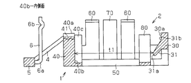
図1に示すように、電子機器は、ハウジングとしての樹脂ケース1を備える。樹脂ケース1は、一体成形品である。樹脂ケース1は、並列に並んでいる複数の収容部2を備えている。そして、収容部2には、電解コンデンサ3が収容されている。なお、図1においては、収容部2の内部構造を図示するため、電解コンデンサ3を収容していない状態の収容部2も一部図示している。
Hereinafter, an embodiment embodying the present invention will be described with reference to FIGS.
As shown in FIG. 1, the electronic device includes a
電解コンデンサ3は、円筒状のボディ部10と、リード20とを備えている。ボディ部10の前端部10aからは一対のリード20が突出している。また、ボディ部10は、リード20の突出側と反対側の端部である後端部10bに図示しない防爆弁を備えている。防爆弁は、後端部10bの中央に配置されている。
The
リード20は、可撓性を有する金属端子であるとともに、略L字状に曲がっている。一対のリード20は、所定間隔をあけて互いに平行に設けられている。
図1に示すように、樹脂ケース1は、ボディ部10の前端部10aと対向するように壁部としての前壁40が設けられ、ボディ部10の後端部10bと対向するように後壁30が設けられている。そして、前壁40と後壁30との間には、支持部50が設けられている。支持部50は、収容部2毎に一対ずつ設けられるとともに前壁40と後壁30とを連結している。すなわち、支持部50は、前壁40及び後壁30に連続している。支持部50は、前後方向に延びており、一対の支持部50の間には後壁30寄りに載置部80が架設されている。載置部80は、円弧状に湾曲形成されている。また、図2に示すように、前壁40の内側面40bに載置部80と同じ形状の載置部40cが突設されている。載置部40c及び載置部80には、電解コンデンサ3のボディ部10が載置されている。
The
As shown in FIG. 1, the
また、図1に示すように、一対の支持部50のうち一方の支持部50からは第1係合片60が二つ立設され、他方の支持部50からは第2係合片70が一つ立設されている。第1係合片60及び第2係合片70は、弾性変形可能に構成されるとともに、ボディ部10側が凹となるように湾曲形成されている。
Further, as shown in FIG. 1, two first engaging
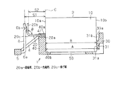
そして、一つの収容部2は、後壁30、前壁40、載置部40c、支持部50、第1係合片60、第2係合片70、載置部80によって構成されている。図3に示すように、収容部2の長手方向寸法A(リード20の突出方向における収容部2の寸法)は、前壁40の内側面40bと後壁30の内側面30aとの距離によって設定されている。収容部2の長手方向寸法Aは、ボディ部10の長手方向寸法B(リード20の突出方向におけるボディ部10の寸法)より大きく設定されているため、ボディ部10と収容部2との間には隙間が存在している。
The single
図2に示すように、後壁30には、収容部2に収容された電解コンデンサ3を前壁40に押し付けるための押し付け部31が設けられており、押し付け部31は、先端部31aが基端部31bより下方に位置するように斜め前方に向かって延出している。押し付け部31は、上方から付勢力が加えられた時には後壁30側に変形するように弾性変形可能になっている。電解コンデンサ3が収容されていない状態における、押し付け部31の先端部31aから前壁40までの距離t1は、ボディ部10の前端部10aからボディ部10の後端部10bまでの距離(ボディ部10の長手方向寸法B)より短くなっている。ボディ部10と収容部2との間には隙間が存在しているが、図3に示すように、電解コンデンサ3が収容部2に収容されている状態において、押し付け部31は、ボディ部10の後端部10bの縁部と当接するとともにボディ部10を前壁40に向けて押圧している。したがって、ボディ部10の前端部10aは、前壁40の内側面40bに押し付けられている。
As shown in FIG. 2, the
後壁30と対向するように前壁40は設けられており、前壁40は、リード20の突出側に位置している。前壁40には、その上面40aの各収容部2と対応する位置に一対のリード20を規制するための規制溝41が形成されている。
The
規制溝41は、前後方向に延設されており、規制溝41の幅は、リード20の直径よりやや大きくなっている。一対の規制溝41の間隔(ピッチ)は、一対のリード20の間隔(ピッチ)と同じとなるように形成されている。そして、規制溝41内には、リード20の一部が配置されている。
The
前壁40の前面には、連結腕部4が複数設けられている。図3に示すように、連結腕部4は、前方に向かって延設されている。そして、図1に示すように、連結腕部4を介して支持棒体5が前壁40と連結されている。支持棒体5は、前壁40の下部と対向する位置において前壁40と平行に設けられるとともに、支持棒体5には、インサート成形によって電極端子としての銅バー6が一体に形成され、銅バー6の基端部6aが支持棒体5に埋め込まれている。
A plurality of connecting
銅バー6は、その基端部6aにおいて略直角に屈曲されて上方に延びている。そして、銅バー6の先端部6bはリード20へ向かって屈曲されており、銅バー6の先端部6bには、リード20へ向かう凸部が形成されている。各収容部2には二つの銅バー6が対応するように配備されている。図3に示すように、銅バー6の先端部6bは、リード20と対向している。そして、リード20の突出側に位置する銅バー6は、リード20と抵抗溶接によって電気的に接続されるように固着されている。リード20は後方に撓んだ状態で銅バー6と固着されている。
The
電子機器を組み立てる際、電解コンデンサ3を樹脂ケース1の収容部2に収容する際に、リード20を規制溝41に入れて収容位置に配置すると、銅バー6に向かって延びている規制溝41がリード20を案内して、自動的にリード20は銅バー6と対向する位置に位置決めされる。また、電解コンデンサ3は押し付け部31により前壁40の内側面40bに押し付けられる。図3に示すように、電解コンデンサ3が収容部2に収容されると、リード20の先端側は銅バー6によって後方へ押圧されるため、リード20の基端部20aからリード20の先端部20bまでの水平成分の距離S1が、電解コンデンサ3が収容される前のリード20の基端部20aからリード20の先端部20bまでの水平成分の距離S2より短くなる。なお、「リード20の基端部20aからリード20の先端部20bまでの水平成分の距離」とは、リード20の基端部20aに垂直な仮想平面Cからリード20の先端部までの距離を意味するものである。そして、リード20は、曲げ部20cより先端側(上側)が後方に撓んだ状態になる。さらに詳述すると、リード20は、曲げ部20cにおける湾曲角度θが少なくとも90度以下となるように撓んだ状態になる。次にリード20を抵抗溶接によって銅バー6の先端部6bと固着させる。
When assembling the electronic device, when the
電解コンデンサ3を収容部2に収容した状態において、銅バー6の先端部6bがリード20を後方に押圧する状態となるように、公差を含めて設計する際、距離S1,S2は電解コンデンサ3の長さに関係なく、前壁40の内側面40bを基準面として決まる。したがって、電解コンデンサ3自体の寸法公差については、考慮に入れる必要がない。
When the
次に前記のように構成された電子機器の作用を説明する。
電解コンデンサ3を収容した電子機器は、収容部2に電解コンデンサ3を収容した状態で車両に搭載される。電子機器が搭載された状態で車両が走行すると、電子機器には振動が加えられる。電子機器に加えられた振動は、電解コンデンサ3にも伝達されるが、電解コンデンサ3は、押し付け部31によってボディ部10が前壁40に押し付けられているため、ボディ部10と後壁30との間に存在している隙間において振動することは抑制される。
Next, the operation of the electronic device configured as described above will be described.
The electronic device that houses the
また、銅バー6を介してリード20に振動が伝達されるとリード20には応力が発生する。しかし、リード20に発生した応力はリード20の曲げ部20cにおいて吸収されるため、リード20の基端部20aに対して集中的に応力が加わることは抑制される。
Further, when vibration is transmitted to the
この実施形態では次の効果を得ることができる。
(1)押し付け部31は、ボディ部10の前端部10aを前壁40の内側面40bに押し付けている。したがって、予め設定された位置に対するリード20と銅バー6とを電気的に接続する接続位置の誤差を小さくすることができる。また、電解コンデンサ3と収容部2との間に存在する隙間において電解コンデンサ3が振動することを抑制できるため、リード20と銅バー6との接続部に負荷がかかって破断することは抑制される。したがって、リード20と銅バー6との接続部の信頼性を向上させることができる。
In this embodiment, the following effects can be obtained.
(1) The
(2)リード20は、曲げ部20cを有するとともに、曲げ部20cより先端側で銅バー6と固着されている。したがって、リード20が振動することによって生じる応力がリード20の曲げ部20cで吸収されるため、リード20に生じた応力がリード20の基端部20aに対して集中的に加わることはない。したがって、電解コンデンサ3が基端部20aから破損することを抑制でき、リード20が真っ直ぐに延出している状態で銅バー6と接続されている場合に比べて、電子機器の耐久性を向上させることができる。
(2) The
(3)電解コンデンサ3が収容部2に収容された状態におけるリード20の基端部20aからリード20の先端部までの水平成分の距離S1は、電解コンデンサ3が収容される前のリード20の基端部20aからリード20の先端部20bまでの距離S2より短くなっている。そして、リード20は銅バー6に押圧されて撓んだ状態で接続されているため、リード20と銅バー6とを互いが離間する方向に力が作用しない状態で接続することができる。また、リード20は銅バー6に押圧されて撓んだ状態で接触しているため、抵抗溶接によってリード20と銅バー6とを電気的に接続する際に、一対の抵抗溶接端子はリード20の突出方向において、リード20と銅バー6の先端部6bとを挟んで加圧できる。したがって、リード20同士の間隔が小さいような電子機器であっても、抵抗溶接を容易に行うことができ、連続的にリード20と銅バー6との接続作業をし易い。
(3) The horizontal component distance S1 from the
(4)前壁40には、その上面40aに規制溝41が形成されており、規制溝41は、リード20を銅バー6へ案内するように銅バー6へ向かって延びている。したがって、リード20を規制溝41に入れて収容位置に配置すると、自動的にリード20が銅バー6へと案内されて銅バー6と対向する位置に位置決めされるため、リード20と銅バー6とを電気的に接続させる接続作業を容易に行うことができる。
(4) A
(5)リード20は、抵抗溶接によって銅バー6と電気的に接続されている。リード20と銅バー6とを抵抗溶接によって電気的に接続すれば、半田付けによってリード20と銅バー6とを電気的に接続する場合に比べて、接続作業時間を短縮することができる。また、溶接時間を短くすることができるため、接続部の周囲に対する熱影響を抑えることができ半田付けによってリード20と銅バー6とを電気的に接続する場合に比べて、品質を向上させることができる。また、放電溶接によってリード20と銅バー6とを電気的に接続すると電解コンデンサ3にサージ電圧が生じ、電解コンデンサ3が破損することがあるが、このような事態が生じることは回避される。
(5) The
(6)押し付け部31は、電解コンデンサ3の後端部10bの縁部を押圧している。したがって、電解コンデンサ3の防爆弁の作動に支障を来たす虞がない。
(7)電解コンデンサ3を収容するハウジングとしては、樹脂ケース1が用いられている。ハウジングとして樹脂ケース1を用いれば、プリント基板に配設される断面積の小さい配線でなく、銅バー6のような断面積の大きい電極端子を容易に用いることができる。したがって、電解コンデンサ3に対して大電流を流しても支障がない。
(6) The
(7) The
(8)電極端子としては、銅バー6が用いられている。プリント基板に配設されるような断面積の小さい配線に大電流を流した場合には、導線に過大な熱が発生し導線自体が損傷するが、電極端子として銅バー6を用いれば、大電流を流しても損傷することはないため、電子機器が許容する電流値の幅を大きくすることができる。
(8) The
(9)収容部2には、第1係合片60と第2係合片70とが設けられている。そして、電解コンデンサ3は、電解コンデンサ3が収容部2に収容された状態において、第1係合片60と第2係合片70とによって係合されているため、電解コンデンサ3の位置ずれを抑制することができる。
(9) The
実施の形態は、前記に限定されるものではなく、例えば、次のように具体化してもよい。
○ リード20と銅バー6とを固着するための方策として抵抗溶接を採用しなくてもよい。すなわち、リード20と銅バー6とは電気的に接続されている状態で固着されればよいため、例えば、放電溶接によってリード20と銅バー6とを固着してもよいし、半田付けによってリード20と銅バー6とを固着してもよい。
The embodiment is not limited to the above, and may be embodied as follows, for example.
O Resistance welding may not be adopted as a measure for fixing the
○ リード20の長さや形状については、変更してもよい。リード20は、銅バー6と電気的に接続することができればよいため、このような目的を達成することができるのであれば、リード20を延長してもよいし、短縮してもよい。また、リード20の径を大きくしてもよいし、径を小さくしてもよい。
○ The length and shape of the
○ L字状に曲がっているリード20を銅バー6と電気的に接続する代わりに、真っ直ぐに延びているリード20を銅バー6と電気的に接続してもよい。この場合、リード20を銅バー6と交差するよう接触させて電気的に接続すればよい。
O Instead of electrically connecting the
○ 電極端子として用いる銅バー6の形状については、リード20と接続することができる形状であればどんな形状でもよい。したがって、例えば、銅バー6の断面形状を扁平形状ではなく、円形状にしてもよい。
The shape of the
○ 電子部品は電解コンデンサ3に限らず、電解コンデンサのような他のリードを備える電子部品に適用してもよい。例えば、コイルや抵抗などを電子部品として使用してもよい。
The electronic component is not limited to the
○ ハウジングとして用いる樹脂ケース1の材質は、絶縁性を有する材質であればよいため、例えば、セラミック製のケースを用いてもよい。
○ 収容部2の大きさや形は電子部品の大きさや形状に対応して変更してもよい。
The material of the
O The size and shape of the
○ 収容部2は、樹脂ケース1に複数設けなくてもよい。すなわち、収容部2は、一つのみでもよい。
○ 押し付け部31は、ボディ部10の後端部10bを押し付けることができるのなら、どのような形状でもよい。例えば、押し付け部31は、側断面半円形状の突起でもよいし、側断面長方形状の突起でもよい。
○ A plurality of
The
○ 押し付け部31は、ボディ部10の後端部10bを押し付けることができるのなら、後壁30に形成されていなくてもよい。例えば、押し付け部31は、支持部50から伸びる形状でもよい。また、押し付け部31が支持部50から伸びる形状である場合には、後壁30を省略してもよい。
The
○ 押し付け部31が押圧する電解コンデンサ3の後端部10bの位置は、後端部10bの縁部であればどの位置でもよい。したがって、例えば、押し付け部31が後端部10bの上側縁部を押圧するように構成してもよい。
The position of the
○ リード20の曲がり具合については特に限定しない。リード20は、電子部品の耐久性向上に寄与できる程度、すなわち、銅バー6から振動が伝達された際に撓んで応力を吸収できる程度に曲げられていればよい。
○ The bending of the
○ 規制溝41を設ける位置や形状は、一対のリード20の間隔やリード20の形状に対応して変更してもよい。また、規制溝41を設けなくてもよい。規制溝41を設けない場合には、例えば、作業者がリード20を保持してリード20が銅バー6と対向するように位置決めしたうえでリード20と銅バー6とを電気的に接続すればよい。
The position and shape of the
○ 電子部品として防爆弁を備えていない場合には、押し付け部31が押圧する部位は、電子部品のリード20の突出側と反対側端部の縁部を押えなくてよい。例えば、押し付け部31によって電子部品のリード20の突出側と反対側端部の中央を押圧してもよい。
O When the explosion-proof valve is not provided as an electronic component, the portion pressed by the
以下の技術的思想は、前記実施形態から把握できる。
(1) 前記ハウジングは、一体成形されていることを特徴とする請求項1〜請求項7のいずれか一項に記載の電子機器。
The following technical idea can be understood from the embodiment.
(1) The electronic apparatus according to any one of
(2) 前記ハウジングは、前記電子部品を収容する収容部を複数備えることを特徴とする請求項1〜請求項7及び(1)のいずれか一項に記載の電子機器。
(3) 前記リードの突出方向における前記収容部の寸法は、前記リードの突出方向における前記電子部品の寸法より大きいことを特徴とする(2)に記載の電子機器。
(2) The electronic device according to any one of
(3) The electronic device according to (2), wherein a dimension of the housing portion in the protruding direction of the lead is larger than a dimension of the electronic component in the protruding direction of the lead.
A…収容部の長手方向寸法、B…ボディ部の長手方向寸法、C…仮想平面、S1…距離、S2…距離、t1…距離、1…ハウジングとしての樹脂ケース、2…収容部、3…電子部品としての電解コンデンサ、6…電極端子としての銅バー、6a…基端部、6b…先端部、10…ボディ部、20…リード、20a…基端部、20b…先端部、20c…曲げ部、31…押し付け部、31a…先端部、31b…基端部、40…壁部としての前壁、40a…上面、40b…内側面、41…規制溝、50…支持部。
A: Longitudinal dimension of housing part, B: Longitudinal dimension of body part, C: Virtual plane, S1: Distance, S2: Distance, t1: Distance, 1 ... Resin case as housing, 2 ... Housing part, 3 ... Electrolytic capacitor as electronic component, 6 ... Copper bar as electrode terminal, 6a ... Base end, 6b ... Tip, 10 ... Body, 20 ... Lead, 20a ... Base end, 20b ... Tip, 20c ...
Claims (7)
前記ハウジングは、前記リードの突出側に位置する壁部と、前記壁部に連続するとともに前記電子部品を支持する支持部とを備え、前記電極端子が前記電子部品のリードの突出側に設けられ、前記ハウジングは、前記電子部品を前記リードの突出側に向けて押圧して前記壁部の前記電極端子側の面に押し付ける押し付け部をさらに備え、
前記リードは、前記電子部品が収容されることにより前記電極端子と電気的に接続されていることを特徴とする電子機器。 An electronic device including a housing in which an electronic component including a lead is accommodated and an electrode terminal,
The housing includes a wall portion located on a protruding side of the lead, and a support portion that is continuous with the wall portion and supports the electronic component, and the electrode terminal is provided on the protruding side of the lead of the electronic component. The housing further includes a pressing portion that presses the electronic component toward the protruding side of the lead and presses the electronic component against the surface of the wall portion on the electrode terminal side,
The electronic device is characterized in that the lead is electrically connected to the electrode terminal by accommodating the electronic component.
Priority Applications (1)
| Application Number | Priority Date | Filing Date | Title |
|---|---|---|---|
| JP2006105532A JP2007281187A (en) | 2006-04-06 | 2006-04-06 | Electronic apparatus |
Applications Claiming Priority (1)
| Application Number | Priority Date | Filing Date | Title |
|---|---|---|---|
| JP2006105532A JP2007281187A (en) | 2006-04-06 | 2006-04-06 | Electronic apparatus |
Publications (1)
| Publication Number | Publication Date |
|---|---|
| JP2007281187A true JP2007281187A (en) | 2007-10-25 |
Family
ID=38682336
Family Applications (1)
| Application Number | Title | Priority Date | Filing Date |
|---|---|---|---|
| JP2006105532A Pending JP2007281187A (en) | 2006-04-06 | 2006-04-06 | Electronic apparatus |
Country Status (1)
| Country | Link |
|---|---|
| JP (1) | JP2007281187A (en) |
Cited By (5)
| Publication number | Priority date | Publication date | Assignee | Title |
|---|---|---|---|---|
| JP2010199397A (en) * | 2009-02-26 | 2010-09-09 | Kitagawa Ind Co Ltd | Holding component |
| JP2015163034A (en) * | 2014-02-28 | 2015-09-07 | 新電元工業株式会社 | Electronic part module and method of manufacturing the same |
| JP2017118041A (en) * | 2015-12-25 | 2017-06-29 | Kyb株式会社 | Electronic component holder |
| WO2017199748A1 (en) * | 2016-05-19 | 2017-11-23 | 株式会社オートネットワーク技術研究所 | Power supply device and method for manufacturing same |
| CN114963520A (en) * | 2021-06-02 | 2022-08-30 | 青岛经济技术开发区海尔热水器有限公司 | Cylindrical capacitor assembly structure and assembly method thereof and heat pump water heater |
-
2006
- 2006-04-06 JP JP2006105532A patent/JP2007281187A/en active Pending
Cited By (9)
| Publication number | Priority date | Publication date | Assignee | Title |
|---|---|---|---|---|
| JP2010199397A (en) * | 2009-02-26 | 2010-09-09 | Kitagawa Ind Co Ltd | Holding component |
| JP2015163034A (en) * | 2014-02-28 | 2015-09-07 | 新電元工業株式会社 | Electronic part module and method of manufacturing the same |
| JP2017118041A (en) * | 2015-12-25 | 2017-06-29 | Kyb株式会社 | Electronic component holder |
| WO2017110265A1 (en) * | 2015-12-25 | 2017-06-29 | Kyb株式会社 | Electronic component holder |
| CN108475578A (en) * | 2015-12-25 | 2018-08-31 | Kyb株式会社 | electronic component holder |
| WO2017199748A1 (en) * | 2016-05-19 | 2017-11-23 | 株式会社オートネットワーク技術研究所 | Power supply device and method for manufacturing same |
| JP2017208481A (en) * | 2016-05-19 | 2017-11-24 | 株式会社オートネットワーク技術研究所 | Power supply device and manufacturing method thereof |
| US10464510B2 (en) | 2016-05-19 | 2019-11-05 | Sumitomo Wiring Systems, Ltd. | Power supply device and method for producing the same |
| CN114963520A (en) * | 2021-06-02 | 2022-08-30 | 青岛经济技术开发区海尔热水器有限公司 | Cylindrical capacitor assembly structure and assembly method thereof and heat pump water heater |
Similar Documents
| Publication | Publication Date | Title |
|---|---|---|
| JP6970875B2 (en) | Capacitor | |
| JP4580999B2 (en) | Motor control unit | |
| US8382512B2 (en) | Flat cable connector, harness, and method for manufacturing harness | |
| CN101093920A (en) | Electronic equipment and method of manufacturing the electronic equipment | |
| CN105900303B (en) | Electric connection box and connector shell | |
| JP6501116B2 (en) | Electrical connection box | |
| CN111989797B (en) | wiring module | |
| CN106463934B (en) | Electrical connection box | |
| JP6993383B2 (en) | Temperature sensor mounting structure | |
| US8254126B2 (en) | Electronic circuit device | |
| WO2013054727A1 (en) | Power supply control device | |
| WO2017168932A1 (en) | Bus bar unit and electronic apparatus provided with bus bar unit | |
| JP5348495B2 (en) | Circuit structure and electrical junction box | |
| WO2014034801A1 (en) | Structure for holding voltage detecting terminal | |
| WO2016002749A1 (en) | Electrical junction box | |
| CN114556685B (en) | Wiring module | |
| JP5950013B2 (en) | Terminal module | |
| JP5080326B2 (en) | Terminal connection structure of electronic component, control unit structure of electric power steering device, and terminal connection method of electronic component | |
| JP5171866B2 (en) | Electronic equipment | |
| CN112400361B (en) | Substrate structure | |
| JP5531565B2 (en) | Electrical junction box and method of manufacturing electrical junction box | |
| JP4844131B2 (en) | Circuit assembly and electrical junction box | |
| JP4442219B2 (en) | Lighting device | |
| US8142205B2 (en) | Electronic apparatus | |
| JP6512451B2 (en) | Power supply |