JP2008218655A - Nitride semiconductor forming substrate, nitride semiconductor using the substrate, and manufacturing method thereof - Google Patents
Nitride semiconductor forming substrate, nitride semiconductor using the substrate, and manufacturing method thereof Download PDFInfo
- Publication number
- JP2008218655A JP2008218655A JP2007053129A JP2007053129A JP2008218655A JP 2008218655 A JP2008218655 A JP 2008218655A JP 2007053129 A JP2007053129 A JP 2007053129A JP 2007053129 A JP2007053129 A JP 2007053129A JP 2008218655 A JP2008218655 A JP 2008218655A
- Authority
- JP
- Japan
- Prior art keywords
- nitride semiconductor
- substrate
- silicon layer
- forming
- porous silicon
- Prior art date
- Legal status (The legal status is an assumption and is not a legal conclusion. Google has not performed a legal analysis and makes no representation as to the accuracy of the status listed.)
- Pending
Links
- 239000000758 substrate Substances 0.000 title claims abstract description 98
- 239000004065 semiconductor Substances 0.000 title claims abstract description 74
- 150000004767 nitrides Chemical class 0.000 title claims abstract description 70
- 238000004519 manufacturing process Methods 0.000 title claims abstract description 19
- 229910021426 porous silicon Inorganic materials 0.000 claims abstract description 89
- XUIMIQQOPSSXEZ-UHFFFAOYSA-N Silicon Chemical compound [Si] XUIMIQQOPSSXEZ-UHFFFAOYSA-N 0.000 claims abstract description 55
- 229910052710 silicon Inorganic materials 0.000 claims abstract description 54
- 239000010703 silicon Substances 0.000 claims abstract description 54
- 239000013078 crystal Substances 0.000 claims abstract description 40
- 239000010409 thin film Substances 0.000 claims abstract description 35
- 239000010408 film Substances 0.000 claims abstract description 21
- 238000000034 method Methods 0.000 claims abstract description 17
- 238000007743 anodising Methods 0.000 claims abstract description 8
- 239000008151 electrolyte solution Substances 0.000 claims abstract description 5
- 239000003792 electrolyte Substances 0.000 claims abstract description 4
- KRHYYFGTRYWZRS-UHFFFAOYSA-N Fluorane Chemical compound F KRHYYFGTRYWZRS-UHFFFAOYSA-N 0.000 claims description 19
- 150000001875 compounds Chemical class 0.000 claims description 7
- LFQSCWFLJHTTHZ-UHFFFAOYSA-N Ethanol Chemical compound CCO LFQSCWFLJHTTHZ-UHFFFAOYSA-N 0.000 claims description 6
- 230000015572 biosynthetic process Effects 0.000 claims description 6
- 239000011259 mixed solution Substances 0.000 claims description 3
- 239000000463 material Substances 0.000 abstract description 2
- 239000010410 layer Substances 0.000 description 91
- 230000008646 thermal stress Effects 0.000 description 8
- 239000011148 porous material Substances 0.000 description 7
- 230000003647 oxidation Effects 0.000 description 6
- 238000007254 oxidation reaction Methods 0.000 description 6
- 230000035882 stress Effects 0.000 description 6
- IJGRMHOSHXDMSA-UHFFFAOYSA-N Atomic nitrogen Chemical compound N#N IJGRMHOSHXDMSA-UHFFFAOYSA-N 0.000 description 5
- 230000007547 defect Effects 0.000 description 4
- 235000019441 ethanol Nutrition 0.000 description 4
- 239000001257 hydrogen Substances 0.000 description 4
- 229910052739 hydrogen Inorganic materials 0.000 description 4
- BASFCYQUMIYNBI-UHFFFAOYSA-N platinum Chemical compound [Pt] BASFCYQUMIYNBI-UHFFFAOYSA-N 0.000 description 4
- 230000000694 effects Effects 0.000 description 3
- 238000005868 electrolysis reaction Methods 0.000 description 3
- 229910052594 sapphire Inorganic materials 0.000 description 3
- 239000010980 sapphire Substances 0.000 description 3
- ZOXJGFHDIHLPTG-UHFFFAOYSA-N Boron Chemical compound [B] ZOXJGFHDIHLPTG-UHFFFAOYSA-N 0.000 description 2
- UFHFLCQGNIYNRP-UHFFFAOYSA-N Hydrogen Chemical compound [H][H] UFHFLCQGNIYNRP-UHFFFAOYSA-N 0.000 description 2
- 229910008310 Si—Ge Inorganic materials 0.000 description 2
- 238000002048 anodisation reaction Methods 0.000 description 2
- 229910052796 boron Inorganic materials 0.000 description 2
- 230000003247 decreasing effect Effects 0.000 description 2
- 238000002248 hydride vapour-phase epitaxy Methods 0.000 description 2
- 150000002431 hydrogen Chemical class 0.000 description 2
- 229910052757 nitrogen Inorganic materials 0.000 description 2
- 229910052697 platinum Inorganic materials 0.000 description 2
- 239000002994 raw material Substances 0.000 description 2
- 238000001953 recrystallisation Methods 0.000 description 2
- 239000002344 surface layer Substances 0.000 description 2
- JLTRXTDYQLMHGR-UHFFFAOYSA-N trimethylaluminium Chemical compound C[Al](C)C JLTRXTDYQLMHGR-UHFFFAOYSA-N 0.000 description 2
- XCZXGTMEAKBVPV-UHFFFAOYSA-N trimethylgallium Chemical compound C[Ga](C)C XCZXGTMEAKBVPV-UHFFFAOYSA-N 0.000 description 2
- OAICVXFJPJFONN-UHFFFAOYSA-N Phosphorus Chemical compound [P] OAICVXFJPJFONN-UHFFFAOYSA-N 0.000 description 1
- 230000002411 adverse Effects 0.000 description 1
- 229910052787 antimony Inorganic materials 0.000 description 1
- WATWJIUSRGPENY-UHFFFAOYSA-N antimony atom Chemical compound [Sb] WATWJIUSRGPENY-UHFFFAOYSA-N 0.000 description 1
- 229910052785 arsenic Inorganic materials 0.000 description 1
- RQNWIZPPADIBDY-UHFFFAOYSA-N arsenic atom Chemical compound [As] RQNWIZPPADIBDY-UHFFFAOYSA-N 0.000 description 1
- 125000004429 atom Chemical group 0.000 description 1
- 239000012159 carrier gas Substances 0.000 description 1
- 238000006243 chemical reaction Methods 0.000 description 1
- 238000005229 chemical vapour deposition Methods 0.000 description 1
- 230000000052 comparative effect Effects 0.000 description 1
- 238000005336 cracking Methods 0.000 description 1
- 230000006866 deterioration Effects 0.000 description 1
- 239000003085 diluting agent Substances 0.000 description 1
- 229910001873 dinitrogen Inorganic materials 0.000 description 1
- 238000004090 dissolution Methods 0.000 description 1
- 239000007789 gas Substances 0.000 description 1
- 229910000040 hydrogen fluoride Inorganic materials 0.000 description 1
- 239000012212 insulator Substances 0.000 description 1
- 238000011835 investigation Methods 0.000 description 1
- 238000004943 liquid phase epitaxy Methods 0.000 description 1
- 229910052751 metal Inorganic materials 0.000 description 1
- 239000002184 metal Substances 0.000 description 1
- 238000001451 molecular beam epitaxy Methods 0.000 description 1
- 229910052698 phosphorus Inorganic materials 0.000 description 1
- 239000011574 phosphorus Substances 0.000 description 1
- 239000000243 solution Substances 0.000 description 1
- 239000002904 solvent Substances 0.000 description 1
- 238000001179 sorption measurement Methods 0.000 description 1
- 230000008022 sublimation Effects 0.000 description 1
- 238000000859 sublimation Methods 0.000 description 1
- 230000003746 surface roughness Effects 0.000 description 1
- 238000010301 surface-oxidation reaction Methods 0.000 description 1
- 238000000927 vapour-phase epitaxy Methods 0.000 description 1
- XLYOFNOQVPJJNP-UHFFFAOYSA-N water Substances O XLYOFNOQVPJJNP-UHFFFAOYSA-N 0.000 description 1
Images
Landscapes
- Weting (AREA)
Abstract
【課題】 シリコン基板上への窒化物半導体薄膜成長時における、各材料間の格子定数差および熱膨張係数差から生じる、該薄膜の歪み、および熱応力に伴うクラック・反りの問題を低減した、窒化物半導体薄膜形成に好適な窒化物半導体薄膜形成用基板を提供すること。
【解決手段】 シリコン単結晶基板片面上に、相対的に多孔度の高い第2多孔質シリコン層および酸化膜除去された相対的に多孔度の低い第1多孔質シリコン層が順次設けられてなることを特徴とする窒素化物半導体形成用基板およびシリコン単結晶基板片面を、電解液中で相対的に低い電流密度で陽極酸化することによって、相対的に低い多孔度の第1多孔質シリコン層を形成する工程、電解液中で相対的に高い電流密度で陽極酸化することによって、シリコン単結晶基板と前記第1シリコン層の間に相対的に高い多孔度の第2多孔質シリコン層を形成する工程、前記第1多孔質層シリコン層および第2多孔質シリコン層を形成した後、酸化膜を除去する工程を含む窒化物半導体形成用基板の製造法。
【選択図】 図1
PROBLEM TO BE SOLVED: To reduce the problem of cracks and warpage caused by thermal distortion and thin film distortion caused by difference in lattice constant and thermal expansion coefficient between materials during growth of a nitride semiconductor thin film on a silicon substrate. To provide a nitride semiconductor thin film forming substrate suitable for forming a nitride semiconductor thin film.
A second porous silicon layer having a relatively high porosity and a first porous silicon layer having a relatively low porosity removed from an oxide film are sequentially provided on one surface of a silicon single crystal substrate. A first porous silicon layer having a relatively low porosity is formed by anodizing a nitride semiconductor forming substrate and a silicon single crystal substrate on one side in an electrolyte at a relatively low current density. Forming a second porous silicon layer having a relatively high porosity between the silicon single crystal substrate and the first silicon layer by anodizing at a relatively high current density in the electrolytic solution; A method for manufacturing a substrate for forming a nitride semiconductor, comprising: a step of removing an oxide film after forming the first porous layer silicon layer and the second porous silicon layer.
[Selection] Figure 1
Description
本発明は、窒素化物半導体形成用基板に関し、更に詳細には、その上に窒素化物半導体皮膜を形成しても、クラック・反り等の生じにくい窒素化物半導体形成用基板、当該基板を用いてなる窒化物半導体及びその製造法に関する。 The present invention relates to a substrate for forming a nitride semiconductor, and more specifically, using a substrate for forming a nitride semiconductor that hardly causes cracking or warping even when a nitride semiconductor film is formed thereon, and the substrate. The present invention relates to a nitride semiconductor and a manufacturing method thereof.
従来、GaNをはじめとする窒化物半導体は、格子整合した基板が高価なために、格子定数の異なる基板上に形成される。現在、GaN形成用基板としては、シリコンと比較してコストの高いサファイアが一般的に用いられているが、これは主に以下のような理由によるものと考えられる。 Conventionally, nitride semiconductors such as GaN are formed on substrates having different lattice constants because lattice-matched substrates are expensive. At present, sapphire, which is more expensive than silicon, is generally used as a substrate for GaN formation, and this is mainly due to the following reasons.
すなわち、通常のc面サファイア(c軸に平行な熱膨張係数7.5×10⁻⁶[K−1])上へのc面GaN(c軸に平行な熱膨張係数5.59×10⁻⁶[K−1])の成長の場合、サファイアの熱膨張係数はGaNより大きいため、結晶成長後の降温時にはGaNに面内圧縮応力が生ずる。そして、一般的に、面内圧縮応力は引っ張り応力に比べクラックを生じさせにくいので、4μm以上のGaNの厚膜形成が可能となる。また、基板とGaN層の界面付近には格子定数差に起因した結晶欠陥が集中する領域があるが、厚膜形成によりデバイス動作層を欠陥が集中した領域から遠ざけることができ、デバイス動作に悪影響を与える結晶欠陥の影響を回避できる。 That is, c-plane GaN (thermal expansion coefficient parallel to c-axis 5.59 × 10 − on parallel c-plane sapphire (thermal expansion coefficient 7.5 × 10 −6 [K −1 ] parallel to c-axis)) In the case of growth of 6 [K −1 ]), since the thermal expansion coefficient of sapphire is larger than that of GaN, in-plane compressive stress is generated in GaN when the temperature is lowered after crystal growth. In general, since the in-plane compressive stress is less likely to cause cracks than the tensile stress, a GaN thick film of 4 μm or more can be formed. In addition, there is a region where crystal defects due to the difference in lattice constant are concentrated near the interface between the substrate and the GaN layer, but the device operation layer can be moved away from the region where defects are concentrated by forming a thick film, which adversely affects device operation. It is possible to avoid the influence of crystal defects that give
一方シリコンを基板とした場合には、熱膨張係数(2.4×10⁻⁶[K−1])がGaNよりも小さいため、結晶成長後の降温時にはGaNに引っ張り応力が生じる。この引っ張り応力は、クラックを発生しやすく、更に夫々の膨張係数の差が大きいことから、極度の凹型反りを発生させ、GaNの厚膜形成が難しく、結晶欠陥の低減が困難となっている。 On the other hand, when silicon is used as the substrate, since the thermal expansion coefficient (2.4 × 10 −6 [K −1 ]) is smaller than that of GaN, tensile stress is generated in GaN when the temperature is lowered after crystal growth. This tensile stress is liable to generate cracks and has a large difference in expansion coefficient between them, which causes extreme concave warpage, making it difficult to form a thick GaN film and reducing crystal defects.
これらの問題を回避し、よりコストの安いシリコンを基板として利用するために、特許文献1においては、多孔質シリコン層の多孔質構造を、細孔径が1nm〜10μm、厚みが3nm〜10μm、多孔度が10%〜90%とコントロールすることで格子不整合を緩和し、良好な結晶性を維持できるとしている。 In order to avoid these problems and to use cheaper silicon as a substrate, in Patent Document 1, the porous structure of the porous silicon layer has a pore diameter of 1 nm to 10 μm, a thickness of 3 nm to 10 μm, and a porous structure. By controlling the degree to 10% to 90%, it is said that the lattice mismatch can be relaxed and good crystallinity can be maintained.
一方、特許文献2においては、多孔質シリコン層の細孔径を3nm以上10nm以下、厚みを0.1μm以上10μm以下、多孔度を0超、0.7以下とすることで、格子不整合、ならびに熱応力を緩和し、クラックの数が減少されるとしている。 On the other hand, in Patent Document 2, the pore size of the porous silicon layer is 3 nm or more and 10 nm or less, the thickness is 0.1 μm or more and 10 μm or less, and the porosity is more than 0 or 0.7 or less, It is said that the number of cracks is reduced by relieving thermal stress.
しかし、特許文献1および2のいずれの技術でも、格子不整合の抑制のために、細孔径を小さくして多孔度を下げれば、熱応力緩和に必要な多孔質シリコン層の構造的脆さを十分に稼げず、クラック・反りの抑制に対して十分な効果が発揮されないという問題があった。一方、多孔度を大きくし過ぎると、多孔質シリコン層の孔構造変化に伴って、化合物半導体薄膜表面が荒れて結晶性が低下してしまう。したがって、格子不整合緩和と熱応力緩和の双方を達成することが困難であるという問題があった。 However, in both techniques of Patent Documents 1 and 2, the structural brittleness of the porous silicon layer necessary for thermal stress relaxation can be reduced by reducing the pore diameter and decreasing the porosity in order to suppress lattice mismatch. There was a problem that it was not able to earn enough, and a sufficient effect was not exhibited for suppressing cracks and warpage. On the other hand, if the porosity is too large, the surface of the compound semiconductor thin film is roughened and the crystallinity is lowered with the change in the pore structure of the porous silicon layer. Therefore, there is a problem that it is difficult to achieve both lattice mismatch relaxation and thermal stress relaxation.
また、特許文献3には、化合物半導体エピタキシャル成長用多孔質シリコン層を、結晶成長面側は低多孔度とし、内部を高多孔度とした2層構造を用いることが開示されている。しかし、この多孔質シリコン層は、基板と化合物半導体薄膜を基板より分離するために用いられるのみのものであり、熱応力緩和への利用は示唆さえされていない。
更に、特許文献4には、化合物半導体(Si−Ge)との格子不整合を緩和するために、基板表層に形成した多孔質シリコン層の多孔度を、表層から内部へ連続的もしくは段階的に変化させ、多孔質層表面をSi−Geの結晶層へと還元性雰囲気下で再結晶化し、再結晶層に生じる格子歪みを内部多孔質シリコン層で緩和することが開示されている。しかし、一般に、再結晶化は、水素などの還元ガス雰囲気下の高温処理が必須となり、水分の存在で面荒れが発生するため、高度な設備とノウハウが必要であり、また、コスト高になるという問題があった。更に、上記特許文献には、上記技術の熱応力緩和への利用は開示されていない。
本発明は、上記実情に鑑みなされたものであり、シリコン基板上への窒化物半導体薄膜の成長時における、各材料間の格子定数差および熱膨張係数差から生じる、該薄膜の歪み、および熱応力に伴うクラック・反りの問題を低減した、窒化物半導体薄膜形成に好適な窒化物半導体薄膜形成用基板を提供することをその課題とするものである。 The present invention has been made in view of the above circumstances, and distortion of the thin film and heat generated from the difference in lattice constant and thermal expansion coefficient between materials during the growth of the nitride semiconductor thin film on the silicon substrate. An object of the present invention is to provide a substrate for forming a nitride semiconductor thin film suitable for forming a nitride semiconductor thin film, in which the problem of cracks and warpage due to stress is reduced.
本願発明者らは、上記課題を解決すべく鋭意検討を重ねた結果、シリコン単結晶基体上に、異なる多孔質構造を有するシリコン層を組み合わせ設けたものを基板とし、更に、その表面から酸化膜を排除することにより、窒化物半導体形成用基板として極めて優れたものが得られることを見出し、本発明を完成するに至った。 As a result of intensive investigations to solve the above problems, the inventors of the present application made a silicon single crystal substrate combined with a silicon layer having a different porous structure as a substrate, and an oxide film from the surface thereof. As a result, it was found that a very excellent substrate for forming a nitride semiconductor can be obtained, and the present invention has been completed.
すなわち本発明は、シリコン単結晶基板片面上に、相対的に多孔度の高い第2多孔質シリコン層および酸化膜除去された相対的に多孔度の低い第1多孔質シリコン層が順次設けられてなることを特徴とする窒素化物半導体形成用基板である。 That is, according to the present invention, a second porous silicon layer having a relatively high porosity and a first porous silicon layer having a relatively low porosity removed from an oxide film are sequentially provided on one surface of a silicon single crystal substrate. This is a nitride semiconductor forming substrate.
また本発明は、シリコン単結晶基板片面を、電解液中で相対的に低い電流密度で陽極酸化することによって、相対的に低い多孔度の第1多孔質シリコン層を形成する工程、電解液中で相対的に高い電流密度で陽極酸化することによって、シリコン単結晶基板と前記第1多孔質シリコン層の間に相対的に高い多孔度の第2多孔質シリコン層を形成する工程、前記第1多孔質シリコン層および第2多孔質シリコン層を形成した後、酸化膜を除去する工程を含む窒化物半導体形成用基板の製造法である。 The present invention also provides a step of forming a first porous silicon layer having a relatively low porosity by anodizing one surface of a silicon single crystal substrate at a relatively low current density in the electrolyte. Forming a second porous silicon layer having a relatively high porosity between the silicon single crystal substrate and the first porous silicon layer by anodizing at a relatively high current density in the first step, This is a method for manufacturing a nitride semiconductor forming substrate including a step of removing an oxide film after forming a porous silicon layer and a second porous silicon layer.
更に本発明は、前記窒化物半導体形成用基板を利用する窒化物半導体および上記窒化物半導体形成用基板の製造法を利用する窒化物半導体薄膜の製造法である。 Furthermore, the present invention relates to a nitride semiconductor using the nitride semiconductor forming substrate and a method for manufacturing a nitride semiconductor thin film using the method for manufacturing the nitride semiconductor forming substrate.
本発明の窒化物半導体形成用基板は、その上でGaNをはじめとする窒化物半導体を成長させ、薄膜を形成させても、窒化物半導体の格子歪みや、熱応力に伴うクラック、反り等を低減させることができ、シリコン基板上の窒化物半導体素子を高性能化することができる。 The nitride semiconductor forming substrate of the present invention grows a nitride semiconductor such as GaN on the substrate and forms a thin film, thereby causing lattice distortion of the nitride semiconductor, cracks and warpage associated with thermal stress, etc. Therefore, the performance of the nitride semiconductor device on the silicon substrate can be improved.
また、本発明の窒化物半導体形成用基板の製造法や、これを利用する窒化物半導体薄膜の製造法では、還元雰囲気下での再結晶化処理が不要となり、製造コストが減少するため、経済性に優れた方法として、窒化物半導体の製造に利用可能性が大きいものである。 Further, in the method for manufacturing a nitride semiconductor forming substrate of the present invention and the method for manufacturing a nitride semiconductor thin film using the same, recrystallization treatment under a reducing atmosphere is unnecessary, and the manufacturing cost is reduced. As an excellent method, the method is highly applicable to the production of nitride semiconductors.
本明細書中において、「相対的に」とは、対応する相手側と比べた場合の大小を意味する。例えば、「相対的に多孔度の高い第2多孔質シリコン層」とは、対応する第1多孔質シリコン層より多孔度が高いことを意味する。同様に、前段の陽極酸化について「相対的に低い電流密度」とは、対応する後段の陽極酸化より、電流密度が低いことを意味する。なお、本発明において、第2多孔質シリコン層では、単一の多孔度の多孔質シリコン層のみならず、複数の異なる多孔度の多孔質シリコン層も含むが、この場合は、平均多孔度を意味する。また本明細書中での多孔度とは、多孔質シリコン層の体積に対する孔体積の比を意味する。 In the present specification, “relatively” means the size when compared with the corresponding counterpart. For example, “a relatively porous second porous silicon layer” means that the porosity is higher than that of the corresponding first porous silicon layer. Similarly, “relatively low current density” for the former stage anodization means that the current density is lower than the corresponding latter stage anodization. In the present invention, the second porous silicon layer includes not only a single porous silicon layer but also a plurality of different porous silicon layers. In this case, the average porosity is means. Moreover, the porosity in this specification means the ratio of the pore volume to the volume of the porous silicon layer.
本発明の窒化物半導体形成用基板は、例えば、電解液中で、裏面に電極を取り付けたシリコン単結晶基板を陽極、白金を陰極とし、シリコン単結晶基板を陽極酸化することにより得られる。 The substrate for forming a nitride semiconductor of the present invention can be obtained, for example, by anodizing a silicon single crystal substrate in an electrolytic solution using a silicon single crystal substrate with an electrode attached to the back surface as an anode and platinum as a cathode.
すなわち、上記陽極酸化においては、まず、シリコン単結晶基板片面上を相対的に低い電流密度で電解することにより、相対的に多孔度の低い第1多孔質シリコン層が形成される。ついで相対的に高い電流密度に変えて、第1多孔質シリコン層が形成されたシリコン単結晶基板を陽極酸化することにより、シリコン単結晶基板上に相対的に高多孔度の第2多孔質シリコン層を形成することができる。 That is, in the anodic oxidation, first, a first porous silicon layer having a relatively low porosity is formed by electrolysis on one surface of a silicon single crystal substrate at a relatively low current density. Next, the second porous silicon having a relatively high porosity is formed on the silicon single crystal substrate by anodizing the silicon single crystal substrate on which the first porous silicon layer is formed in place of the relatively high current density. A layer can be formed.
この陽極酸化は、例えば、フッ化水素酸とアルコール等、好ましくは、フッ化水素酸とエチルアルコールの混液を電解液として実施することができる。このフッ化水素酸とアルコールの比は、特に制約されるものではないが、30質量%のフッ化水素酸とアルコールの比が、1:1〜2:1であることが好ましい。 This anodic oxidation can be performed using, for example, a hydrofluoric acid and alcohol, preferably a mixed solution of hydrofluoric acid and ethyl alcohol as an electrolytic solution. The ratio of hydrofluoric acid to alcohol is not particularly limited, but the ratio of 30% by mass of hydrofluoric acid to alcohol is preferably 1: 1 to 2: 1.
本発明において原料として用いられるシリコン単結晶基板としては、ボロン、リン、アンチモン、ヒ素や他の元素をドープしたものが利用できる。またその厚みは、0.3ないし2mmであることが好ましい。厚みが0.3mm未満の場合、基板の反りが大きすぎて不都合であり、また厚みが2mm超の場合、シリコン単結晶インゴットよりスライス可能な基板枚数が減少して非効率的である。 As the silicon single crystal substrate used as a raw material in the present invention, a substrate doped with boron, phosphorus, antimony, arsenic or other elements can be used. The thickness is preferably 0.3 to 2 mm. When the thickness is less than 0.3 mm, the warpage of the substrate is too large, which is inconvenient. When the thickness is more than 2 mm, the number of slicable substrates is less than that of the silicon single crystal ingot, which is inefficient.
一方、陽極酸化により、シリコン結晶基板上に形成される、第1多孔質シリコン層および第2多孔質シリコン層の多孔度及び厚みは、電流密度や、時間を変えることで制御可能である。具体的には、電流密度が高いほど、陽極酸化により多孔度が高くなり、また、時間が長いほど 膜厚が厚くなる。実際の実施に当たっては、これらの関係を実験的に確認し、これに基づいて条件を定めればよい。 On the other hand, the porosity and thickness of the first porous silicon layer and the second porous silicon layer formed on the silicon crystal substrate by anodic oxidation can be controlled by changing the current density and time. Specifically, the higher the current density, the higher the porosity due to anodic oxidation, and the longer the time, the thicker the film thickness. In actual implementation, these relationships may be confirmed experimentally, and conditions may be determined based on this.
前記のシリコン単結晶基板上の第1多孔質シリコン層は、その多孔度が0.1ないし3%であることが好ましく、また、その厚みも、0.1ないし2μmであることが好ましい。このような多孔度、膜厚の条件を満たす第1多孔質シリコン層を形成させる電解条件の一例としては、電流密度が0.1ないし1mA/cm2、好ましくは、1mA/cm2の条件を挙げることができる。 The first porous silicon layer on the silicon single crystal substrate preferably has a porosity of 0.1 to 3% and a thickness of 0.1 to 2 μm. As an example of the electrolysis conditions for forming the first porous silicon layer satisfying such conditions of porosity and film thickness, the current density is 0.1 to 1 mA / cm 2 , preferably 1 mA / cm 2 . Can be mentioned.
このようにして得られる第1多孔質シリコン層は、その多孔度が低く、膜厚が薄い方が窒化物半導体薄膜の成長に適している。例えば、多孔度が3%超の場合、窒化物半導体薄膜成長時の孔構造変化により、結晶成長面が荒れて、該薄膜にクラックが発生し、不都合である。また、厚みが前記範囲外では、GaN成長時の第2多孔質シリコン層の構造変化に影響されてクラックが発生するので不都合である。 The first porous silicon layer thus obtained has a lower porosity and a smaller thickness is suitable for growing a nitride semiconductor thin film. For example, when the porosity is more than 3%, the crystal growth surface is rough due to the change in the pore structure during the growth of the nitride semiconductor thin film, and cracks are generated in the thin film. On the other hand, if the thickness is out of the above range, it is inconvenient because cracks occur due to the structural change of the second porous silicon layer during GaN growth.
また、前記第2多孔質シリコン層は、多孔度が20ないし50%、好ましくは、30ないし50%で、厚みが10μmないし60μm、好ましくは、20ないし25μmである。このような多孔度、膜厚の第2多孔質シリコン層を形成させるための電解条件としては、の例としては、電流密度1ないし50mA/cm2を挙げることができる。 The second porous silicon layer has a porosity of 20 to 50%, preferably 30 to 50%, and a thickness of 10 to 60 μm, preferably 20 to 25 μm. Examples of electrolysis conditions for forming the second porous silicon layer having such a porosity and film thickness include a current density of 1 to 50 mA / cm 2 .
第2多孔質シリコン層は、多孔度や厚みを上記範囲に調整することにより、格子歪みおよび熱応力の緩和に効果を発揮することができ、クラック・反りを低減できる。第2シリコン層の厚みが10μm未満の場合、熱応力緩和が不十分となってクラック・反りが生じ、また60μm超の場合、孔構造が著しく変化して、窒化物半導体薄膜が割れて剥離し、不都合である。 By adjusting the porosity and thickness of the second porous silicon layer to the above ranges, the second porous silicon layer can exert an effect on relaxation of lattice strain and thermal stress, and can reduce cracks and warpage. If the thickness of the second silicon layer is less than 10 μm, thermal stress relaxation becomes insufficient and cracks and warpage occur, and if it exceeds 60 μm, the pore structure changes significantly and the nitride semiconductor thin film is cracked and peeled off. Inconvenient.
なお、上記第2多孔質シリコン層は、抵抗が106Ωcm以上、107Ωcm以下の半絶縁体であり、例えば、GaN結晶を用いた高周波トランジスタの用途においては、該多孔質層が抵抗層として機能するため有用である。 The second porous silicon layer is a semi-insulator having a resistance of 10 6 Ωcm or more and 10 7 Ωcm or less. For example, in the use of a high-frequency transistor using a GaN crystal, the porous layer is a resistance layer. It is useful because it functions as
上記した第2多孔質シリコン層は、上記記載の多孔度の範囲内で、高多孔度の層と低多孔度の層を交互に少なくとも一層積層させた構造でもよい。このような構造は、第2多孔質シリコン層を形成する陽極酸化の際に、一定時間電流密度を変化させることにより、簡単に形成することができる。すなわち、高多孔度の層を形成する場合は、電流密度を高く、低多孔度の層を形成する場合は、電流密度を低くすればよい。そして、高多孔度である第2多孔質シリコン層の中に存在する低多孔度層は、第1多孔質シリコン層の過度の構造変化を抑制し、第1多孔質シリコン層上に形成される窒化物半導体薄膜の結晶品質の低下を阻止できる。 The above-mentioned second porous silicon layer may have a structure in which at least one layer of high porosity and low porosity are alternately laminated within the above-described range of porosity. Such a structure can be easily formed by changing the current density for a certain time during the anodic oxidation for forming the second porous silicon layer. That is, when forming a highly porous layer, the current density may be increased, and when forming a low porosity layer, the current density may be decreased. And the low-porosity layer which exists in the 2nd porous silicon layer which is high porosity suppresses the excessive structural change of a 1st porous silicon layer, and is formed on a 1st porous silicon layer. The deterioration of the crystal quality of the nitride semiconductor thin film can be prevented.
さらに、第2多孔質シリコン層が、垂直方向に、多孔度の高い部分から多孔度の低い部分、あるいは多孔度の低い部分から多孔度の高い部分へと、連続的あるいは段階的に変化する構造であっても良い。このような構造も、第2多孔質シリコン層を形成する陽極酸化の際に、電流密度を連続的あるいは段階的に変化させることにより、簡単に形成することができ、上記記載と同様の効果を得ることができる。 Further, the second porous silicon layer has a structure in which the second porous silicon layer is changed continuously or stepwise from a high porosity portion to a low porosity portion, or from a low porosity portion to a high porosity portion in the vertical direction. It may be. Such a structure can also be easily formed by changing the current density continuously or stepwise during the anodic oxidation for forming the second porous silicon layer, and has the same effect as described above. Obtainable.
上記のように、表面に第1および第2多孔質シリコン層が形成されたシリコン単結晶基板は、さらにその多孔質シリコン層表面からの酸化膜除去と、水素終端化のための処理が行われる。この処理は、窒化物半導体薄膜成長において存在が問題となる酸化膜を除去し、酸化され難い多孔質シリコン層表面構造を形成するためであり、窒化物半導体結晶成長に適した表面構造を得るために重要なものである。 As described above, the silicon single crystal substrate having the first and second porous silicon layers formed on the surface is further subjected to the treatment for removing the oxide film from the surface of the porous silicon layer and hydrogen termination. . This treatment is for removing an oxide film that is problematic in the growth of nitride semiconductor thin films, and forming a porous silicon layer surface structure that is difficult to oxidize, in order to obtain a surface structure suitable for nitride semiconductor crystal growth. It is important to.
この処理は、例えば、フッ化水素酸を用いて行うことができ、特に、50〜40質量%程度のフッ化水素酸で行うことが好ましい。この際、濃度の低いフッ化水素酸を用いた場合、希釈溶媒である水による多孔質表面酸化とフッ化水素による溶解が繰り返されるため、多孔質シリコン層の表面が荒れ、不都合である。 This treatment can be performed using, for example, hydrofluoric acid, and is particularly preferably performed with about 50 to 40% by mass of hydrofluoric acid. At this time, when hydrofluoric acid having a low concentration is used, porous surface oxidation with water as a diluent solvent and dissolution with hydrogen fluoride are repeated, which is inconvenient because the surface of the porous silicon layer becomes rough.
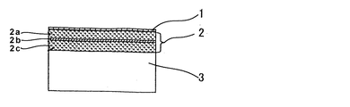
以上の処理が終わった状態の、本発明の窒化物半導体形成用基板の一態様の模式図を、図1に示す。図中、1は酸化膜除去および水素終端化された第1多孔質シリコン層、2は第2多孔質シリコン層、3はシリコン結晶基板である。 FIG. 1 shows a schematic view of one embodiment of the nitride semiconductor forming substrate of the present invention after the above processing is completed. In the figure, 1 is a first porous silicon layer from which an oxide film is removed and hydrogen-terminated, 2 is a second porous silicon layer, and 3 is a silicon crystal substrate.
図1に示すように、本発明の窒化物半導体形成用基板は、シリコン結晶基板3の上に、第2多孔質シリコン層2および酸化膜除去および水素終端化された第1多孔質シリコン層1が順次設けられた構造になっている。また、第2多孔質シリコン層2は、その中が基板1側から、高多孔質層2c、低多孔質層2b、高多孔質層2aの積層構造となっている。このように積層構造にすることにより、低多孔質層2bが第2多孔質シリコン層の強度を高め、変形を防ぐことが可能となるのである。
As shown in FIG. 1, the substrate for forming a nitride semiconductor of the present invention has a second porous silicon layer 2 and a first porous silicon layer 1 which is oxide-removed and hydrogen-terminated on a
かくして得られた本発明の窒化物半導体形成用基体上に、窒化物半導体薄膜を成長、形成させるには、公知の技術を用いることができ、特に限定されない。公知の技術としては、常圧有機金属気相成長法(MOCVD法)、分子線エピタキシー法(MBE法)、ハイドライド気相成長法(HVPE法)、昇華法、液相成長法等があげられる。 In order to grow and form the nitride semiconductor thin film on the nitride semiconductor forming substrate of the present invention thus obtained, a known technique can be used, and there is no particular limitation. Known techniques include atmospheric pressure metalorganic vapor phase epitaxy (MOCVD), molecular beam epitaxy (MBE), hydride vapor phase epitaxy (HVPE), sublimation and liquid phase epitaxy.
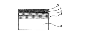
このように、本発明の窒化物半導体形成用基板上に、GaN結晶を成長させた状態を模式的に図2に示す。図2に示すGaN結晶の成長工程は、常圧有機金属気相成長法(MOCVD法)によるもので、第1多孔質シリコン層1上に、初期層としてAlN層4を成長、形成させた後、GaN層5を成長、形成させたものである。
FIG. 2 schematically shows a state in which a GaN crystal is grown on the nitride semiconductor formation substrate of the present invention. The GaN crystal growth step shown in FIG. 2 is performed by atmospheric pressure metal organic chemical vapor deposition (MOCVD), and after an AlN layer 4 is grown and formed as an initial layer on the first porous silicon layer 1.
本発明の窒化物半導体形成用基体は、種々の窒化物半導体薄膜を成長、形成させることが可能であるが、このうち、好ましいもの例として、下記一般式
BXAlYGa(1−X−Y−Z)InZN
(式中、0≦X≦1、0≦Y≦1、0≦Z≦1)
で表される化合物を挙げることができる。
The nitride semiconductor-forming substrate of the present invention can grow and form various nitride semiconductor thin films. Among these, as preferred examples, the following general formula B X Al Y Ga (1-X— Y-Z) In Z N
(Where 0 ≦ X ≦ 1, 0 ≦ Y ≦ 1, 0 ≦ Z ≦ 1)
The compound represented by these can be mentioned.
次に実施例を挙げ、本発明を更に詳しく説明するが、本発明はこれら実施例により何ら制約されるものではない。 EXAMPLES Next, although an Example is given and this invention is demonstrated in more detail, this invention is not restrict | limited at all by these Examples.
実 施 例 1
次に、シリコン単結晶基板片面上に、厚さ0.46μmの第1多孔質シリコン層と、第1シリコン層下のシリコン単結晶基板に形成された、厚さ24μmの第2多孔質シリコン層とからなる2種類の多孔質シリコン層が形成されたシリコン単結晶基板上にGaN層を製造させる方法の一例を実施例として説明する。
Example 1
Next, a first porous silicon layer having a thickness of 0.46 μm and a second porous silicon layer having a thickness of 24 μm formed on the silicon single crystal substrate below the first silicon layer on one surface of the silicon single crystal substrate. An example of a method for producing a GaN layer on a silicon single crystal substrate on which two types of porous silicon layers comprising:
電解液である30質量%フッ化水素酸−エチルアルコール混合液(容量比1:1))中、ボロンが5×10¹⁸atoms/cm3でドープされ、比抵抗値が0.01ΩcmのP型シリコン(111)を陽極、白金電極を陰極として、電流密度1mA/cm2で4分間通電して、P型シリコン上に第1多孔質シリコン層を形成させた。この第1多孔質シリコン層の多孔度は、1%であり、その厚みは0.46μmであった。尚、多孔度の測定は窒素ガス吸着法にて行った。 Boron is doped at 5 × 10 18 atoms / cm 3 in a 30% by mass hydrofluoric acid-ethyl alcohol mixed solution (capacity ratio 1: 1), which is an electrolytic solution, and a specific resistance value is 0.01 Ωcm. Using silicon (111) as an anode and a platinum electrode as a cathode, current was passed at a current density of 1 mA / cm 2 for 4 minutes to form a first porous silicon layer on P-type silicon. This first porous silicon layer had a porosity of 1% and a thickness of 0.46 μm. The porosity was measured by a nitrogen gas adsorption method.
その後、更に電流密度21mA/cm2で8分、電流密度1mA/cm2で4分、電流密度21mA/cm2で8分間通電して、第1多孔質シリコン層下のシリコン単結晶基板上面に、第2多孔質シリコン層を形成させ、本発明の窒化物半導体形成用シリコン基板を作製した。この第2多孔質シリコン層の多孔度は、50%であり、その厚みは24μmであった。 Thereafter, further 8 minutes at a current density of 21 mA / cm 2, 4 minutes at a current density of 1 mA / cm 2, by energizing a current density 21 mA / cm 2 8 min, the silicon single crystal substrate top surface under the first porous silicon layer Then, a second porous silicon layer was formed, and a silicon substrate for forming a nitride semiconductor of the present invention was produced. This second porous silicon layer had a porosity of 50% and a thickness of 24 μm.
更に、第1および第2多孔質シリコン層が形成されたシリコン基板を、50重量%HF液に1分間浸して酸化膜を除去した。その結果、表面が水素終端化された第1多孔質シリコン層を有するシリコン基板が得られた。 Furthermore, the silicon substrate on which the first and second porous silicon layers were formed was immersed in 50 wt% HF solution for 1 minute to remove the oxide film. As a result, a silicon substrate having a first porous silicon layer whose surface was hydrogen-terminated was obtained.
次に、作製した該シリコン基板を、MOCVD装置の反応炉内にセットし、成膜を行った。まず、窒素および水素の混合キャリアガス(窒素10L/min、水素7.5L/min)を流しながら、該シリコン基板温度を1150℃とし、第2多孔質シリコン層表面のサーマルクリーニングを行った。ついで、該シリコン基板の温度を1120℃とし、反応炉内にトリメチルアルミニウム(TMA)を17μmol/min、NH3を2.5L/minで供給し、第1多孔質シリコン層上に、厚さ50nmのAlN薄膜を成長させた。 Next, the produced silicon substrate was set in a reactor of a MOCVD apparatus, and film formation was performed. First, while flowing a mixed carrier gas of nitrogen and hydrogen (nitrogen 10 L / min, hydrogen 7.5 L / min), the silicon substrate temperature was set to 1150 ° C., and the surface of the second porous silicon layer was thermally cleaned. Next, the temperature of the silicon substrate was set to 1120 ° C., trimethylaluminum (TMA) was supplied into the reaction furnace at 17 μmol / min, and NH 3 was supplied at 2.5 L / min, and a thickness of 50 nm was formed on the first porous silicon layer. An AlN thin film was grown.
続いて、シリコン基板の温度は1120℃で、トリメチルガリウム(TMG)69μmol/min、NH3を2.5L/minで供給し、AlN上に、厚さ1μmのGaN薄膜を成長させた。 Subsequently, the temperature of the silicon substrate was 1120 ° C., trimethylgallium (TMG) was supplied at 69 μmol / min, and NH 3 was supplied at 2.5 L / min to grow a GaN thin film having a thickness of 1 μm on AlN.
成長させたGaN表面は鏡面状であり、ノルマルスキー顕微鏡(100倍)を用いてその表面を観察したが、クラックやビットは認められなかった。また、一片が約2cmの正三角形状と半径約2cm、中心角60度の扇形状の基板をレーザー測長器で測定したところ、GaN形成させた後の反りは2.6μmであった。 The grown GaN surface was mirror-like, and the surface was observed using a normalsky microscope (100 times), but no cracks or bits were observed. Further, when a fan-shaped substrate having a regular triangle shape of about 2 cm, a radius of about 2 cm, and a central angle of 60 degrees was measured with a laser length measuring instrument, the warp after forming GaN was 2.6 μm.
比 較 例 1
本発明の多孔化処理したシリコン基板の代わりに、洗浄した面方位(111)のシリコン基板(原料シリコン板)を用いた以外は、実施例1と同様にして、シリコン基板上に、厚さ50nmのAlN薄膜及び厚さ1μmのGaN薄膜を順次成長させた。
Comparative Example 1
A thickness of 50 nm is formed on the silicon substrate in the same manner as in Example 1 except that a silicon substrate (raw material silicon plate) having a cleaned plane orientation (111) is used instead of the porous silicon substrate of the present invention. The AlN thin film and the GaN thin film having a thickness of 1 μm were sequentially grown.
成長させたGaN表面は鏡面状であったが、ノルマルスキー顕微鏡(100倍)を用いて観察したしたところ、クラックが認められた。また、実施例1と同様に、レーザー測長器で基板を測定したところ、GaN形成させた後の反りは10μmであった。 The grown GaN surface was specular, but cracks were observed when observed using a normalsky microscope (100 times). Further, when the substrate was measured with a laser length measuring device in the same manner as in Example 1, the warpage after forming GaN was 10 μm.
本発明では、シリコン基板上に表面平坦性や結晶性に優れた窒化物半導体薄膜を成長させることができ、シリコン基板上の窒化物半導体素子を高性能化することができる。 In the present invention, a nitride semiconductor thin film having excellent surface flatness and crystallinity can be grown on a silicon substrate, and the performance of the nitride semiconductor device on the silicon substrate can be improved.
1 … … 酸化膜除去された第1多孔質シリコン層
2 … … 第2多孔質シリコン層
3 … … シリコン基板
4 … … AlN薄膜
5 … … GaN薄膜
DESCRIPTION OF SYMBOLS 1 ...... The 1st porous silicon layer from which the oxide film was removed 2 ...... The 2nd
Claims (16)
BXAlYGa(1−X−Y−Z)InZN
(式中、0≦X≦1、0≦Y≦1、0≦Z≦1)
で表される化合物で形成されたものである請求項第8項記載の窒化物半導体。 The nitride semiconductor thin film has the following formula: B X Al Y Ga (1-XYZ) In Z N
(Where 0 ≦ X ≦ 1, 0 ≦ Y ≦ 1, 0 ≦ Z ≦ 1)
The nitride semiconductor according to claim 8, which is formed of a compound represented by the formula:
BXAlYGa(1−X−Y−Z)InZN
(式中、0≦X≦1、0≦Y≦1、0≦Z≦1)
で表される化合物で形成されたものである請求項第15項記載の窒化物半導体薄膜の製造法。
The nitride semiconductor thin film has the following formula: B X Al Y Ga (1-XYZ) In Z N
(Where 0 ≦ X ≦ 1, 0 ≦ Y ≦ 1, 0 ≦ Z ≦ 1)
The method for producing a nitride semiconductor thin film according to claim 15, wherein the nitride semiconductor thin film is formed of a compound represented by the formula:
Priority Applications (1)
| Application Number | Priority Date | Filing Date | Title |
|---|---|---|---|
| JP2007053129A JP2008218655A (en) | 2007-03-02 | 2007-03-02 | Nitride semiconductor forming substrate, nitride semiconductor using the substrate, and manufacturing method thereof |
Applications Claiming Priority (1)
| Application Number | Priority Date | Filing Date | Title |
|---|---|---|---|
| JP2007053129A JP2008218655A (en) | 2007-03-02 | 2007-03-02 | Nitride semiconductor forming substrate, nitride semiconductor using the substrate, and manufacturing method thereof |
Publications (1)
| Publication Number | Publication Date |
|---|---|
| JP2008218655A true JP2008218655A (en) | 2008-09-18 |
Family
ID=39838353
Family Applications (1)
| Application Number | Title | Priority Date | Filing Date |
|---|---|---|---|
| JP2007053129A Pending JP2008218655A (en) | 2007-03-02 | 2007-03-02 | Nitride semiconductor forming substrate, nitride semiconductor using the substrate, and manufacturing method thereof |
Country Status (1)
| Country | Link |
|---|---|
| JP (1) | JP2008218655A (en) |
Cited By (2)
| Publication number | Priority date | Publication date | Assignee | Title |
|---|---|---|---|---|
| JP2010165934A (en) * | 2009-01-16 | 2010-07-29 | Furukawa Electric Co Ltd:The | Semiconductor electronic device |
| CN105789026A (en) * | 2014-12-25 | 2016-07-20 | 中国科学院微电子研究所 | Substrate structure and manufacturing method thereof |
Citations (6)
| Publication number | Priority date | Publication date | Assignee | Title |
|---|---|---|---|---|
| JPH0536669A (en) * | 1991-07-30 | 1993-02-12 | Nippondenso Co Ltd | Method for manufacturing semiconductor device |
| JPH10321535A (en) * | 1997-03-17 | 1998-12-04 | Canon Inc | Semiconductor substrate having compound semiconductor layer, method of manufacturing the same, and electronic device manufactured on the semiconductor substrate |
| JPH11195562A (en) * | 1997-12-26 | 1999-07-21 | Sony Corp | Semiconductor substrate, thin film semiconductor member, and method of manufacturing the same |
| JP2003282464A (en) * | 2002-03-27 | 2003-10-03 | Seiko Epson Corp | Semiconductor substrate and method of manufacturing the same |
| JP2005129876A (en) * | 2003-10-22 | 2005-05-19 | Sc Technology Kk | Method of laminating compound semiconductor material |
| JP2005210097A (en) * | 2003-12-22 | 2005-08-04 | Interuniv Micro Electronica Centrum Vzw | Method and apparatus for growing a group III nitride material on a silicon substrate |
-
2007
- 2007-03-02 JP JP2007053129A patent/JP2008218655A/en active Pending
Patent Citations (6)
| Publication number | Priority date | Publication date | Assignee | Title |
|---|---|---|---|---|
| JPH0536669A (en) * | 1991-07-30 | 1993-02-12 | Nippondenso Co Ltd | Method for manufacturing semiconductor device |
| JPH10321535A (en) * | 1997-03-17 | 1998-12-04 | Canon Inc | Semiconductor substrate having compound semiconductor layer, method of manufacturing the same, and electronic device manufactured on the semiconductor substrate |
| JPH11195562A (en) * | 1997-12-26 | 1999-07-21 | Sony Corp | Semiconductor substrate, thin film semiconductor member, and method of manufacturing the same |
| JP2003282464A (en) * | 2002-03-27 | 2003-10-03 | Seiko Epson Corp | Semiconductor substrate and method of manufacturing the same |
| JP2005129876A (en) * | 2003-10-22 | 2005-05-19 | Sc Technology Kk | Method of laminating compound semiconductor material |
| JP2005210097A (en) * | 2003-12-22 | 2005-08-04 | Interuniv Micro Electronica Centrum Vzw | Method and apparatus for growing a group III nitride material on a silicon substrate |
Cited By (2)
| Publication number | Priority date | Publication date | Assignee | Title |
|---|---|---|---|---|
| JP2010165934A (en) * | 2009-01-16 | 2010-07-29 | Furukawa Electric Co Ltd:The | Semiconductor electronic device |
| CN105789026A (en) * | 2014-12-25 | 2016-07-20 | 中国科学院微电子研究所 | Substrate structure and manufacturing method thereof |
Similar Documents
| Publication | Publication Date | Title |
|---|---|---|
| JP3886341B2 (en) | Method for manufacturing gallium nitride crystal substrate and gallium nitride crystal substrate | |
| JP4597259B2 (en) | Group III nitride semiconductor growth substrate, group III nitride semiconductor epitaxial substrate, group III nitride semiconductor device, group III nitride semiconductor free-standing substrate, and methods of manufacturing the same | |
| JP4117156B2 (en) | Method for manufacturing group III nitride semiconductor substrate | |
| US20090057835A1 (en) | Group III nitride semiconductor and a manufacturing method thereof | |
| CN102465342B (en) | Method of manufacturing gan-based film | |
| CN102465343A (en) | Method of manufacturing gan-based film | |
| US9896780B2 (en) | Method for pretreatment of base substrate and method for manufacturing layered body using pretreated base substrate | |
| JP2012009483A (en) | Semiconductor element manufacturing method, laminated structure manufacturing method, and semiconductor wafer and laminated structure | |
| JP2006062931A (en) | Sapphire substrate, heat treatment method thereof, and crystal growth method | |
| JP4768759B2 (en) | Group III nitride semiconductor substrate | |
| JP5230522B2 (en) | Manufacturing method of laminated body and semiconductor device having the laminated body | |
| JP2002299267A (en) | Semiconductor substrate manufacturing method | |
| KR101358541B1 (en) | Ⅲ-nitride semiconductor growth substrate, ⅲ-nitride semiconductor epitaxial substrate, ⅲ-nitride semiconductor element, ⅲ-nitride semiconductor freestanding substrate, and method for fabricating these | |
| JP2020075842A (en) | Nitride semiconductor | |
| JP2008218655A (en) | Nitride semiconductor forming substrate, nitride semiconductor using the substrate, and manufacturing method thereof | |
| JP2010225947A (en) | Nitride-semiconductor forming substrate and method of manufacturing the same | |
| JP5430467B2 (en) | Group III nitride semiconductor growth substrate, group III nitride semiconductor free-standing substrate, group III nitride semiconductor device, and methods of manufacturing the same | |
| JP5684551B2 (en) | Group III nitride semiconductor growth substrate, group III nitride semiconductor epitaxial substrate, group III nitride semiconductor device, group III nitride semiconductor free-standing substrate, and methods of manufacturing the same | |
| JP2018065711A (en) | Group III nitride semiconductor substrate and method for manufacturing group III nitride semiconductor substrate | |
| TW201513176A (en) | Semiconductor wafer and method of producing semiconductor wafer | |
| JP2017214232A (en) | Method of manufacturing nitride compound semiconductor substrate | |
| JP2010278470A (en) | Substrate for growing group-iii nitride semiconductor, epitaxial substrate for group-iii nitride semiconductor, group-iii nitride semiconductor element, stand-alone substrate for group-iii nitride semiconductor, and methods for manufacturing the same | |
| JP4507810B2 (en) | Nitride semiconductor substrate manufacturing method and nitride semiconductor substrate | |
| JP2008308349A (en) | Group III nitride single crystal manufacturing method, base crystal substrate having metal nitride layer, and multilayer structure wafer | |
| JP2005340379A (en) | Compound semiconductor and manufacturing method thereof |
Legal Events
| Date | Code | Title | Description |
|---|---|---|---|
| A621 | Written request for application examination |
Effective date: 20100208 Free format text: JAPANESE INTERMEDIATE CODE: A621 |
|
| RD02 | Notification of acceptance of power of attorney |
Free format text: JAPANESE INTERMEDIATE CODE: A7422 Effective date: 20100218 |
|
| A521 | Written amendment |
Free format text: JAPANESE INTERMEDIATE CODE: A821 Effective date: 20100218 |
|
| A977 | Report on retrieval |
Effective date: 20111129 Free format text: JAPANESE INTERMEDIATE CODE: A971007 |
|
| A02 | Decision of refusal |
Free format text: JAPANESE INTERMEDIATE CODE: A02 Effective date: 20120403 |