JP2009005178A - チョッパ型コンパレータ - Google Patents
チョッパ型コンパレータ Download PDFInfo
- Publication number
- JP2009005178A JP2009005178A JP2007165341A JP2007165341A JP2009005178A JP 2009005178 A JP2009005178 A JP 2009005178A JP 2007165341 A JP2007165341 A JP 2007165341A JP 2007165341 A JP2007165341 A JP 2007165341A JP 2009005178 A JP2009005178 A JP 2009005178A
- Authority
- JP
- Japan
- Prior art keywords
- comparison
- resistance value
- unit
- voltage
- power supply
- Prior art date
- Legal status (The legal status is an assumption and is not a legal conclusion. Google has not performed a legal analysis and makes no representation as to the accuracy of the status listed.)
- Granted
Links
Images



Classifications
-
- H—ELECTRICITY
- H03—ELECTRONIC CIRCUITRY
- H03K—PULSE TECHNIQUE
- H03K5/00—Manipulating of pulses not covered by one of the other main groups of this subclass
- H03K5/22—Circuits having more than one input and one output for comparing pulses or pulse trains with each other according to input signal characteristics, e.g. slope, integral
- H03K5/24—Circuits having more than one input and one output for comparing pulses or pulse trains with each other according to input signal characteristics, e.g. slope, integral the characteristic being amplitude
-
- H—ELECTRICITY
- H03—ELECTRONIC CIRCUITRY
- H03K—PULSE TECHNIQUE
- H03K5/00—Manipulating of pulses not covered by one of the other main groups of this subclass
- H03K5/01—Shaping pulses
- H03K5/08—Shaping pulses by limiting; by thresholding; by slicing, i.e. combined limiting and thresholding
-
- H—ELECTRICITY
- H03—ELECTRONIC CIRCUITRY
- H03M—CODING; DECODING; CODE CONVERSION IN GENERAL
- H03M1/00—Analogue/digital conversion; Digital/analogue conversion
- H03M1/06—Continuously compensating for, or preventing, undesired influence of physical parameters
- H03M1/0602—Continuously compensating for, or preventing, undesired influence of physical parameters of deviations from the desired transfer characteristic
- H03M1/0604—Continuously compensating for, or preventing, undesired influence of physical parameters of deviations from the desired transfer characteristic at one point, i.e. by adjusting a single reference value, e.g. bias or gain error
- H03M1/0607—Offset or drift compensation
-
- H—ELECTRICITY
- H03—ELECTRONIC CIRCUITRY
- H03M—CODING; DECODING; CODE CONVERSION IN GENERAL
- H03M1/00—Analogue/digital conversion; Digital/analogue conversion
- H03M1/12—Analogue/digital converters
- H03M1/34—Analogue value compared with reference values
- H03M1/38—Analogue value compared with reference values sequentially only, e.g. successive approximation type
- H03M1/46—Analogue value compared with reference values sequentially only, e.g. successive approximation type with digital/analogue converter for supplying reference values to converter
Landscapes
- Physics & Mathematics (AREA)
- Nonlinear Science (AREA)
- Engineering & Computer Science (AREA)
- Theoretical Computer Science (AREA)
- Analogue/Digital Conversion (AREA)
- Manipulation Of Pulses (AREA)
Abstract
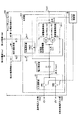
【解決手段】第1の電源が供給される第1の電源供給ラインと、前記第1の電源よりも電圧の低い第2の電源が供給される第2の電源供給ラインと、基準電圧が入力される基準電圧入力部と、比較対象電圧が入力される比較対象電圧入力部と、前記基準電圧入力部から入力される前記基準電圧と前記比較対象電圧入力部から入力される前記比較対象電圧との大小を比較する比較部と、前記比較部の比較結果を出力する出力部とを備えたチョッパ型コンパレータであって、前記第1の電源供給ライン及び/又は前記第2の電源供給ラインの抵抗値を設定する抵抗値設定部を備えたことを特徴とする。
【選択図】図1
Description
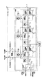
図1は本発明の実施例1のチョッパ型コンパレータ100の回路構成例を示す図である。
図8は本発明の実施例2のチョッパ型コンパレータ300の回路構成例を示す図である。同図中、図1と同一部品については、同一符号を付し、その説明は省略する。図1と異なる部分は、比較部310の構成である。比較部310は、電圧保持部25、35、短絡選択部SW4、SW5、反転型比較増幅器20−2、20−3が追加され、電圧保持部と反転型比較増幅器と短絡選択部が3段直列に接続された構成となっている。抵抗R3、R4、R5、R6、R7、R8は配線等によって生じる抵抗である。また、抵抗値設定部30を構成する抵抗R1、R2は、反転型比較増幅器20−1、20−2、20−3の共通インピーダンスとなる。
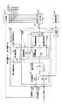
図9は本発明のチョッパ型コンパレータ100を備えたA/D変換器の回路構成例を示す図である。同図中、図1と同一部品については、同一符号を付し、その説明は省略する。図9は、6ビットのA/D変換器の例である。
15 電圧保持部
20−1 反転型比較増幅器
20−2 反転型比較増幅器
20−3 反転型比較増幅器
21 正側電源供給部
22 負側電源供給部
23 PMOS・FET
24 NMOS・FET
25 電圧保持部
30 抵抗値設定部
35 電圧保持部
40 第1の電源供給ライン
50 第2の電源供給ライン
51 正側電源供給部
52 負側電源供給部
60 スイッチ制御部
61 正側電源供給部
62 負側電源供給部
100 チョッパ型コンパレータ
110 比較部
200 チョッパ型コンパレータ
210 比較部
300 チョッパ型コンパレータ
310 比較部
500 D/A変換部
600 レジスタ部
700 変換制御部
R1〜R8 抵抗
C1〜C3 コンデンサ
SW1、SW2 スイッチ
SW3〜SW5 短絡選択部
Vdd 第1の電源
Vss 第2の電源
Vref 基準電圧入力部
Vin0 比較対象電圧入力部
Vin1〜Vin3 入力
Vout0〜Vout3 出力
Iinv、Iinv1〜Iinv3 電流
Vth 閾値電圧
A アナログ電圧
Claims (7)
- 第1の電源が供給される第1の電源供給ラインと、
前記第1の電源よりも電圧の低い第2の電源が供給される第2の電源供給ラインと、
基準電圧が入力される基準電圧入力部と、
比較対象電圧が入力される比較対象電圧入力部と、
前記基準電圧入力部から入力される前記基準電圧と前記比較対象電圧入力部から入力される前記比較対象電圧との大小を比較する比較部と、
前記比較部の比較結果を出力する出力部とを備えたチョッパ型コンパレータであって、
前記第1の電源供給ライン及び/又は前記第2の電源供給ラインの抵抗値を設定する抵抗値設定部を備えたことを特徴とするチョッパ型コンパレータ。 - 前記比較部は、閾値電圧が所定の値である反転型比較増幅器を備え、前記抵抗値設定部の抵抗値は、前記反転型比較増幅器の前記閾値電圧の変動を低減するような抵抗値に設定されることを特徴とする請求項1記載のチョッパ型コンパレータ。
- 前記反転型比較増幅器の前記所定の閾値電圧の変動を低減するような抵抗値は、前記反転型比較増幅器に流れる電流値の変化に基づいて設定されることを特徴とする請求項1又は2記載のチョッパ型コンパレータ。
- 前記抵抗値設定部の抵抗値は、配線により形成された抵抗の抵抗値を含むことを特徴とする請求項1乃至3のいずれか一項に記載のチョッパ型コンパレータ。
- 前記抵抗値設定部の抵抗値は、ボンディングワイヤで形成された抵抗の抵抗値を含むことを特徴とする請求項1乃至4のいずれか一項に記載のチョッパ型コンパレータ。
- 前記抵抗値設定部の抵抗値は、スルーホールで形成された抵抗の抵抗値を含むことを特徴とする請求項1乃至5のいずれか一項に記載のチョッパ型コンパレータ。
- 請求項1乃至6のいずれか一項に記載のチョッパ型コンパレータを備えたA/D変換器。
Priority Applications (5)
| Application Number | Priority Date | Filing Date | Title |
|---|---|---|---|
| JP2007165341A JP5186818B2 (ja) | 2007-06-22 | 2007-06-22 | チョッパ型コンパレータ |
| EP08765265A EP2178209A1 (en) | 2007-06-22 | 2008-06-06 | Chopper-type comparator and a/d converter |
| PCT/JP2008/060452 WO2009001657A1 (ja) | 2007-06-22 | 2008-06-06 | チョッパ型コンパレータ及びa/d変換器 |
| CN200880021131A CN101689850A (zh) | 2007-06-22 | 2008-06-06 | 斩波型比较器以及a/d变换器 |
| US12/665,356 US8149019B2 (en) | 2007-06-22 | 2008-06-06 | Chopper type comparator and A/D converter |
Applications Claiming Priority (1)
| Application Number | Priority Date | Filing Date | Title |
|---|---|---|---|
| JP2007165341A JP5186818B2 (ja) | 2007-06-22 | 2007-06-22 | チョッパ型コンパレータ |
Publications (2)
| Publication Number | Publication Date |
|---|---|
| JP2009005178A true JP2009005178A (ja) | 2009-01-08 |
| JP5186818B2 JP5186818B2 (ja) | 2013-04-24 |
Family
ID=40185478
Family Applications (1)
| Application Number | Title | Priority Date | Filing Date |
|---|---|---|---|
| JP2007165341A Expired - Fee Related JP5186818B2 (ja) | 2007-06-22 | 2007-06-22 | チョッパ型コンパレータ |
Country Status (5)
| Country | Link |
|---|---|
| US (1) | US8149019B2 (ja) |
| EP (1) | EP2178209A1 (ja) |
| JP (1) | JP5186818B2 (ja) |
| CN (1) | CN101689850A (ja) |
| WO (1) | WO2009001657A1 (ja) |
Cited By (1)
| Publication number | Priority date | Publication date | Assignee | Title |
|---|---|---|---|---|
| JP2012145418A (ja) * | 2011-01-11 | 2012-08-02 | Lapis Semiconductor Co Ltd | 半導体回路、半導体装置、断線検出方法、及び断線検出プログラム |
Families Citing this family (2)
| Publication number | Priority date | Publication date | Assignee | Title |
|---|---|---|---|---|
| JP5718067B2 (ja) * | 2011-01-17 | 2015-05-13 | ラピスセミコンダクタ株式会社 | 昇圧システム、診断方法、及び診断プログラム |
| KR20230159144A (ko) | 2022-05-13 | 2023-11-21 | 삼성전자주식회사 | 피드백 회로를 포함하는 비교기 회로 |
Citations (6)
| Publication number | Priority date | Publication date | Assignee | Title |
|---|---|---|---|---|
| JPS63260316A (ja) * | 1987-04-17 | 1988-10-27 | Nec Corp | 発振回路 |
| JPS63276316A (ja) * | 1987-05-07 | 1988-11-14 | Nec Corp | 発振回路 |
| JPH02101814A (ja) * | 1988-10-08 | 1990-04-13 | Sharp Corp | チョッパ型コンパレータ |
| JPH08316801A (ja) * | 1995-05-19 | 1996-11-29 | Sanyo Electric Co Ltd | チョッパインバータ比較器及びa/dコンバータ |
| JPH118534A (ja) * | 1997-06-18 | 1999-01-12 | Seiko Epson Corp | 半導体集積回路 |
| JP2004056649A (ja) * | 2002-07-23 | 2004-02-19 | Renesas Technology Corp | チョッパ型コンパレータおよびそれを用いたad変換器 |
Family Cites Families (9)
| Publication number | Priority date | Publication date | Assignee | Title |
|---|---|---|---|---|
| JPH02124624A (ja) * | 1988-07-04 | 1990-05-11 | Toshiba Corp | インバータ回路及び該回路を用いたチョッパ型コンパレータ回路 |
| JPH05235767A (ja) | 1992-02-20 | 1993-09-10 | Hitachi Ltd | A/d変換器 |
| JP2937027B2 (ja) * | 1994-09-07 | 1999-08-23 | 日本電気株式会社 | コンパレータ |
| JP3529212B2 (ja) * | 1995-12-12 | 2004-05-24 | シャープ株式会社 | 反転増幅回路 |
| JP2001016079A (ja) * | 1999-06-30 | 2001-01-19 | Toshiba Lsi System Support Kk | チョッパ型電圧比較回路 |
| JP3621358B2 (ja) * | 2001-05-25 | 2005-02-16 | Necマイクロシステム株式会社 | コンパレータ及びアナログディジタルコンバータ |
| JP2005057717A (ja) * | 2003-07-23 | 2005-03-03 | Oki Electric Ind Co Ltd | チョッパー型コンパレータ回路 |
| JP2007329518A (ja) * | 2006-06-06 | 2007-12-20 | Oki Electric Ind Co Ltd | チョッパ型コンパレータ |
| JP4825704B2 (ja) | 2007-03-09 | 2011-11-30 | トヨタ自動車株式会社 | 燃料電池発電システムおよびその運転方法 |
-
2007
- 2007-06-22 JP JP2007165341A patent/JP5186818B2/ja not_active Expired - Fee Related
-
2008
- 2008-06-06 US US12/665,356 patent/US8149019B2/en active Active
- 2008-06-06 WO PCT/JP2008/060452 patent/WO2009001657A1/ja not_active Ceased
- 2008-06-06 EP EP08765265A patent/EP2178209A1/en not_active Withdrawn
- 2008-06-06 CN CN200880021131A patent/CN101689850A/zh active Pending
Patent Citations (6)
| Publication number | Priority date | Publication date | Assignee | Title |
|---|---|---|---|---|
| JPS63260316A (ja) * | 1987-04-17 | 1988-10-27 | Nec Corp | 発振回路 |
| JPS63276316A (ja) * | 1987-05-07 | 1988-11-14 | Nec Corp | 発振回路 |
| JPH02101814A (ja) * | 1988-10-08 | 1990-04-13 | Sharp Corp | チョッパ型コンパレータ |
| JPH08316801A (ja) * | 1995-05-19 | 1996-11-29 | Sanyo Electric Co Ltd | チョッパインバータ比較器及びa/dコンバータ |
| JPH118534A (ja) * | 1997-06-18 | 1999-01-12 | Seiko Epson Corp | 半導体集積回路 |
| JP2004056649A (ja) * | 2002-07-23 | 2004-02-19 | Renesas Technology Corp | チョッパ型コンパレータおよびそれを用いたad変換器 |
Cited By (2)
| Publication number | Priority date | Publication date | Assignee | Title |
|---|---|---|---|---|
| JP2012145418A (ja) * | 2011-01-11 | 2012-08-02 | Lapis Semiconductor Co Ltd | 半導体回路、半導体装置、断線検出方法、及び断線検出プログラム |
| US8930159B2 (en) | 2011-01-11 | 2015-01-06 | Lapis Semiconductor Co., Ltd. | Semiconductor circuit, semiconductor device, line break detection method, and computer readable medium storing line break detection program |
Also Published As
| Publication number | Publication date |
|---|---|
| EP2178209A1 (en) | 2010-04-21 |
| WO2009001657A1 (ja) | 2008-12-31 |
| US20100182052A1 (en) | 2010-07-22 |
| US8149019B2 (en) | 2012-04-03 |
| CN101689850A (zh) | 2010-03-31 |
| JP5186818B2 (ja) | 2013-04-24 |
Similar Documents
| Publication | Publication Date | Title |
|---|---|---|
| CN101867373B (zh) | 模拟到数字转换器 | |
| JP7061110B2 (ja) | 高電圧ブートストラップサンプリング回路 | |
| US20090015451A1 (en) | Flash a/d converter | |
| CN101267193A (zh) | 进行电压比较,防止电压比较精度恶化的半导体集成电路 | |
| US20110273231A1 (en) | Semiconductor integrated circuit | |
| US8456343B2 (en) | Switched capacitor type D/A converter | |
| US20080284634A1 (en) | Differential amplifying circuit | |
| JP5186818B2 (ja) | チョッパ型コンパレータ | |
| CN116015256B (zh) | 自带失调消除的比较器 | |
| US20100289936A1 (en) | Buffer circuit, image sensor chip comprising the same, and image pickup device | |
| JP2002118466A (ja) | Ad変換回路 | |
| CN1700598B (zh) | 半导体集成电路 | |
| TWI293521B (en) | Electronic circuit device | |
| CN222638508U (zh) | 运算放大器、调制器和温度传感器 | |
| US7358813B2 (en) | Differential operational amplifier | |
| CN103425168A (zh) | 电压-电流变换器电路 | |
| TWI783245B (zh) | 運算放大器的降電容方案 | |
| US20080191920A1 (en) | Low-voltage drop reference generation circuit for A/D converter | |
| KR101939147B1 (ko) | 가변 기준전압 발생회로 및 이를 포함한 아날로그 디지털 변환기 | |
| JP2008283284A (ja) | Ad変換器 | |
| JP4635612B2 (ja) | サンプル・ホールド回路 | |
| CN110785925A (zh) | 跨导放大器和芯片 | |
| JP2010063072A (ja) | 電圧電流変換回路 | |
| JP4725472B2 (ja) | 引き算回路および演算増幅器 | |
| JP2009171338A (ja) | 減衰補償回路 |
Legal Events
| Date | Code | Title | Description |
|---|---|---|---|
| A621 | Written request for application examination |
Free format text: JAPANESE INTERMEDIATE CODE: A621 Effective date: 20100615 |
|
| A131 | Notification of reasons for refusal |
Free format text: JAPANESE INTERMEDIATE CODE: A131 Effective date: 20120417 |
|
| A521 | Request for written amendment filed |
Free format text: JAPANESE INTERMEDIATE CODE: A523 Effective date: 20120612 |
|
| TRDD | Decision of grant or rejection written | ||
| A01 | Written decision to grant a patent or to grant a registration (utility model) |
Free format text: JAPANESE INTERMEDIATE CODE: A01 Effective date: 20121225 |
|
| A61 | First payment of annual fees (during grant procedure) |
Free format text: JAPANESE INTERMEDIATE CODE: A61 Effective date: 20130107 |
|
| FPAY | Renewal fee payment (event date is renewal date of database) |
Free format text: PAYMENT UNTIL: 20160201 Year of fee payment: 3 |
|
| R150 | Certificate of patent or registration of utility model |
Ref document number: 5186818 Country of ref document: JP Free format text: JAPANESE INTERMEDIATE CODE: R150 Free format text: JAPANESE INTERMEDIATE CODE: R150 |
|
| LAPS | Cancellation because of no payment of annual fees |