JP2009043256A - 記憶装置のアクセス方法及び装置 - Google Patents
記憶装置のアクセス方法及び装置 Download PDFInfo
- Publication number
- JP2009043256A JP2009043256A JP2008200750A JP2008200750A JP2009043256A JP 2009043256 A JP2009043256 A JP 2009043256A JP 2008200750 A JP2008200750 A JP 2008200750A JP 2008200750 A JP2008200750 A JP 2008200750A JP 2009043256 A JP2009043256 A JP 2009043256A
- Authority
- JP
- Japan
- Prior art keywords
- storage device
- main
- interface
- interrupt
- processing
- Prior art date
- Legal status (The legal status is an assumption and is not a legal conclusion. Google has not performed a legal analysis and makes no representation as to the accuracy of the status listed.)
- Granted
Links
Images

Classifications
-
- G—PHYSICS
- G06—COMPUTING OR CALCULATING; COUNTING
- G06F—ELECTRIC DIGITAL DATA PROCESSING
- G06F13/00—Interconnection of, or transfer of information or other signals between, memories, input/output devices or central processing units
- G06F13/14—Handling requests for interconnection or transfer
- G06F13/16—Handling requests for interconnection or transfer for access to memory bus
- G06F13/1605—Handling requests for interconnection or transfer for access to memory bus based on arbitration
- G06F13/1652—Handling requests for interconnection or transfer for access to memory bus based on arbitration in a multiprocessor architecture
- G06F13/1663—Access to shared memory
-
- G—PHYSICS
- G06—COMPUTING OR CALCULATING; COUNTING
- G06F—ELECTRIC DIGITAL DATA PROCESSING
- G06F13/00—Interconnection of, or transfer of information or other signals between, memories, input/output devices or central processing units
- G06F13/14—Handling requests for interconnection or transfer
- G06F13/20—Handling requests for interconnection or transfer for access to input/output bus
- G06F13/24—Handling requests for interconnection or transfer for access to input/output bus using interrupt
Landscapes
- Engineering & Computer Science (AREA)
- Theoretical Computer Science (AREA)
- Physics & Mathematics (AREA)
- General Engineering & Computer Science (AREA)
- General Physics & Mathematics (AREA)
- Multi Processors (AREA)
- Storage Device Security (AREA)
- Bus Control (AREA)
Abstract
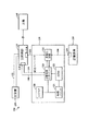
【解決手段】本発明によるシステム装置は、記憶装置、バス、第一主装置、及び第二主装置を有する。記憶装置は自由なハンドシェークプロトコルに合わせた記憶装置インターフェースを有し、該記憶装置インターフェースは記憶装置とアクセス主装置の間にある。バスは記憶装置に電気接続される。第一主装置はバスと記憶装置インターフェースを介して記憶装置をアクセスし、及び割り込みインターフェースを介して割り込み要求を受信した後、割り込み操作を実行する。第二主装置はバスと記憶装置アクセスインターフェースを介して記憶装置をアクセスし、記憶装置をアクセスする前に第一主装置に割り込み要求を伝送する。
【選択図】 図1
Description
102、 第一バス部分
104、 第二バス部分
110、 主制御器(Host Controller)
114、134、 直列周辺インターフェース
118、 割り込みインターフェース
120、 組込コントローラ
121、 処理ユニット
122、 ランダムアクセス記憶装置(RAM)
123、 記憶装置インターフェース
125、 多重化装置
128、 レジスタ
130、 記憶装置
140、 主機(host computer)
144、 配線
146、 線路
154、 主装置
200、202、204、206、208、210、212、230、240、 ステップ
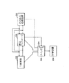
320、 組込コントローラ
322、 スイッチ
324、 開閉器
350、 他の処理装置
Claims (15)
- システム装置であって、
記憶装置とアクセス主装置の間にあり、自由なハンドシェークプロトコルに合わせた記憶装置インターフェースを有する記憶装置と、
該記憶装置に電気接続されたバスと、
該バスと該記憶装置インターフェースを介して該記憶装置をアクセスし、割り込みインターフェースを介して割り込み要求を受信した後、割り込み操作を実行する第一主装置と、
該バスと該記憶装置インターフェースを介して該記憶装置をアクセスし、該記憶装置をアクセスする前に該第一主装置に該割り込み要求を伝送する第二主装置と、
を含むシステム装置。 - 該記憶装置インターフェースは該バスの衝突識別のプロトコルをサポートしないインターフェースを含む請求項1記載のシステム装置。
- 該記憶装置インターフェースはプロトコルインターフェースであり、該プロトコルインターフェースは、直列周辺インターフェースプロトコル又は単一処理装置を選択して記憶装置をアクセスするのをサポートしないプロトコルに従って稼動される、請求項1記載のシステム装置。
- 該第一主装置はコンピューターの主機を有し、該コンピューターの主機は主制御器を介して、少なくとも
(i)該記憶装置をアクセスするステップ、及び
(ii)割り込み要求を受信するステップ
を実行する、請求項1記載のシステム装置。 - 該第一主装置はコンピューターの主機を有し、該第二主装置は該コンピューターの組込コントローラを有する、請求項1記載のシステム装置。
- 該第二主装置はコンピューターの制御器を有し、該制御器はシステム制御器、キーボード制御器又はノートパソコンの組込コントローラである、請求項1記載のシステム装置。
- 該第二主装置は該第一主装置及び該記憶装置に電気接続された該バスに位置する、請求項1記載のシステム装置。
- 該第二主装置は該第一主装置より発送された割り込み確認情報を受信した後、又は該割り込み要求を発送してから所定時間後に記憶装置をアクセスし、該割り込み確認情報は該第一主装置から該割り込み要求に応じて発送された情報である、請求項1記載のシステム装置。
- 該第一主装置と該第二主装置は処理装置を有する、請求項1記載のシステム装置。
- 処理装置であって、
自由なハンドシェークプロトコルに従って記憶装置を制御する記憶装置インターフェースと、
割り込み要求を処理装置に伝送する割り込みインターフェースと、
過程の任務を実行し、該記憶装置インターフェースを介して該記憶装置からデータを読み出し又はデータを該記憶装置に保存し、該割り込みインターフェースを介して該割り込み要求を伝送し、該記憶装置インターフェースを介して該記憶装置をアクセスする前に割り込み確認情報を受信する処理ユニットと、
を含む処理装置。 - 該処理ユニットは割り込みインターフェースとそれぞれ独立したレジスタを介して割り込み確認情報を受信する、請求項10記載の処理装置。
- 該処理ユニットは該記憶装置から符号のブロックを読み出す、請求項10記載の処理装置。
- 前記処理装置は内部記憶装置を有し、該内部記憶装置は処理ユニットより実行されるアプリケーションの部分符号を保存し、該内部記憶装置は該記憶装置インターフェースを介して記憶装置から該符号ブロックを入れ替える、請求項12記載の処理装置。
- 記憶装置をアクセスする方法であって、
少なくとも一つの第一主装置を記憶装置に接続する段階と、
第二主装置から該少なくとも一つの第一主装置に割り込み要求を発送する段階と、
該少なくとも一つの第一主装置より割り込み要求に応じて発送された割り込み確認情報を受信する段階と、
該少なくとも一つの第一主装置が割り込み要求を処理する間に、記憶装置をアクセスする段階と、
を含む記憶装置をアクセスする方法。 - 記憶装置へのアクセスが完了した後、該少なくとも一つの第一主装置の該割り込み要求処理を解放する段階を含む、請求項14記載の記憶装置をアクセスする方法。
Applications Claiming Priority (2)
| Application Number | Priority Date | Filing Date | Title |
|---|---|---|---|
| US11/834,053 US8285895B2 (en) | 2007-08-06 | 2007-08-06 | Handshake free sharing in a computer architecture |
| US11/834,053 | 2007-08-06 |
Publications (2)
| Publication Number | Publication Date |
|---|---|
| JP2009043256A true JP2009043256A (ja) | 2009-02-26 |
| JP4855451B2 JP4855451B2 (ja) | 2012-01-18 |
Family
ID=40347542
Family Applications (1)
| Application Number | Title | Priority Date | Filing Date |
|---|---|---|---|
| JP2008200750A Active JP4855451B2 (ja) | 2007-08-06 | 2008-08-04 | 記憶装置のアクセス方法及び装置 |
Country Status (4)
| Country | Link |
|---|---|
| US (1) | US8285895B2 (ja) |
| JP (1) | JP4855451B2 (ja) |
| CN (1) | CN101364212B (ja) |
| TW (1) | TWI394048B (ja) |
Families Citing this family (14)
| Publication number | Priority date | Publication date | Assignee | Title |
|---|---|---|---|---|
| US20090037932A1 (en) * | 2007-08-01 | 2009-02-05 | Clark Michael T | Mechanism for broadcasting system management interrupts to other processors in a computer system |
| TWI397009B (zh) * | 2009-04-30 | 2013-05-21 | Inventec Corp | 基本輸入輸出系統的資料處理裝置 |
| EP2430528A1 (en) * | 2009-05-15 | 2012-03-21 | Thomson Licensing | System and method for sharing memory |
| US8510492B2 (en) * | 2010-09-08 | 2013-08-13 | Integrated Device Technology Inc. | System and method for communication handshaking between a master processors and a slave processor |
| US9268721B2 (en) | 2010-11-25 | 2016-02-23 | International Business Machines Corporation | Holding by a memory controller multiple central processing unit memory access requests, and performing the multiple central processing unit memory requests in one transfer cycle |
| US9448954B2 (en) * | 2011-02-28 | 2016-09-20 | Dsp Group Ltd. | Method and an apparatus for coherency control |
| CN102999471B (zh) * | 2011-09-09 | 2015-11-04 | 中国科学院声学研究所 | 一种多处理器共享非易失性存储卡的方法及系统 |
| JP5915192B2 (ja) * | 2012-01-12 | 2016-05-11 | ミツミ電機株式会社 | センサ出力補正回路及びセンサ出力補正装置 |
| TWI510903B (zh) * | 2012-11-19 | 2015-12-01 | Wistron Corp | 電腦系統及資料回復方法 |
| US20160350240A1 (en) * | 2015-05-29 | 2016-12-01 | Analog Devices Global | Serial peripheral interface host port |
| US20180373653A1 (en) * | 2017-06-21 | 2018-12-27 | Hewlett Packard Enterprise Development Lp | Commitment of acknowledged data in response to request to commit |
| US10579280B2 (en) * | 2018-06-28 | 2020-03-03 | Montage Technology Co., Ltd. | On-die termination control for memory systems |
| KR102813343B1 (ko) * | 2018-08-06 | 2025-05-27 | 에스케이하이닉스 주식회사 | 데이터 처리 시스템 및 그의 동작 방법 |
| TWI775436B (zh) * | 2021-05-17 | 2022-08-21 | 新唐科技股份有限公司 | 匯流排系統 |
Citations (5)
| Publication number | Priority date | Publication date | Assignee | Title |
|---|---|---|---|---|
| JPS60237566A (ja) * | 1984-05-10 | 1985-11-26 | Oki Electric Ind Co Ltd | プロセツサ間通信方式 |
| JPS6159516A (ja) * | 1984-08-30 | 1986-03-27 | Fujitsu Ltd | タイマ機構 |
| JPH03116335A (ja) * | 1989-09-29 | 1991-05-17 | Oki Electric Ind Co Ltd | 非特権cpuから特権cpuヘの乗り移り方式 |
| JP2003196251A (ja) * | 2001-12-27 | 2003-07-11 | Denso Corp | マルチcpuシステム |
| JP2004528656A (ja) * | 2001-05-16 | 2004-09-16 | インターナショナル・ビジネス・マシーンズ・コーポレーション | 組込み制御環境におけるリモート入出力機能への効率的なアクセスのための方法およびシステム |
Family Cites Families (19)
| Publication number | Priority date | Publication date | Assignee | Title |
|---|---|---|---|---|
| EP0601715A1 (en) | 1992-12-11 | 1994-06-15 | National Semiconductor Corporation | Bus of CPU core optimized for accessing on-chip memory devices |
| US5603055A (en) | 1994-01-27 | 1997-02-11 | Vlsi Technology, Inc. | Single shared ROM for storing keyboard microcontroller code portion and CPU code portion and disabling access to a portion while accessing to the other |
| US5819087A (en) | 1996-07-19 | 1998-10-06 | Compaq Computer Corporation | Flash ROM sharing between processor and microcontroller during booting and handling warm-booting events |
| US5794054A (en) | 1996-07-19 | 1998-08-11 | Compaq Computer Corporation | Flash ROM sharing between a processor and a controller |
| US5892943A (en) | 1996-12-30 | 1999-04-06 | Standard Microsystems Corp. | Shared bios ROM warm boot |
| US5999476A (en) | 1997-11-21 | 1999-12-07 | Advanced Micro Devices, Inc. | Bios memory and multimedia data storage combination |
| US6272584B1 (en) | 1998-09-10 | 2001-08-07 | Compaq Computer Corporation | System board with consolidated EEPROM module |
| US7089339B2 (en) | 2001-03-16 | 2006-08-08 | National Semiconductor Corporation | Sharing of functions between an embedded controller and a host processor |
| US6976136B2 (en) | 2001-05-07 | 2005-12-13 | National Semiconductor Corporation | Flash memory protection scheme for secured shared BIOS implementation in personal computers with an embedded controller |
| TW515959B (en) * | 2001-05-10 | 2003-01-01 | Via Tech Inc | Method for memory data access by system management interrupt and computer system thereof |
| TWI240861B (en) * | 2002-01-11 | 2005-10-01 | Integrated Circuit Solution In | Data access method and architecture of flash memory |
| US8037224B2 (en) * | 2002-10-08 | 2011-10-11 | Netlogic Microsystems, Inc. | Delegating network processor operations to star topology serial bus interfaces |
| US6886089B2 (en) * | 2002-11-15 | 2005-04-26 | Silicon Labs Cp, Inc. | Method and apparatus for accessing paged memory with indirect addressing |
| US7079427B2 (en) * | 2004-07-02 | 2006-07-18 | Taiwan Semiconductor Manufacturing Company, Ltd. | System and method for a high-speed access architecture for semiconductor memory |
| US7814377B2 (en) * | 2004-07-09 | 2010-10-12 | Sandisk Corporation | Non-volatile memory system with self test capability |
| JP2006172142A (ja) * | 2004-12-16 | 2006-06-29 | Matsushita Electric Ind Co Ltd | マルチプロセッサシステム |
| KR100725099B1 (ko) * | 2005-12-22 | 2007-06-04 | 삼성전자주식회사 | 멀티패쓰 억세스블 반도체 메모리 장치에서의 메모리확장구조 |
| US7987464B2 (en) * | 2006-07-25 | 2011-07-26 | International Business Machines Corporation | Logical partitioning and virtualization in a heterogeneous architecture |
| CN101000596A (zh) | 2007-01-22 | 2007-07-18 | 北京中星微电子有限公司 | 一种可实现芯片内多核间通信的芯片及通信方法 |
-
2007
- 2007-08-06 US US11/834,053 patent/US8285895B2/en active Active
-
2008
- 2008-07-24 TW TW097128083A patent/TWI394048B/zh active
- 2008-08-04 CN CN2008101452551A patent/CN101364212B/zh active Active
- 2008-08-04 JP JP2008200750A patent/JP4855451B2/ja active Active
Patent Citations (5)
| Publication number | Priority date | Publication date | Assignee | Title |
|---|---|---|---|---|
| JPS60237566A (ja) * | 1984-05-10 | 1985-11-26 | Oki Electric Ind Co Ltd | プロセツサ間通信方式 |
| JPS6159516A (ja) * | 1984-08-30 | 1986-03-27 | Fujitsu Ltd | タイマ機構 |
| JPH03116335A (ja) * | 1989-09-29 | 1991-05-17 | Oki Electric Ind Co Ltd | 非特権cpuから特権cpuヘの乗り移り方式 |
| JP2004528656A (ja) * | 2001-05-16 | 2004-09-16 | インターナショナル・ビジネス・マシーンズ・コーポレーション | 組込み制御環境におけるリモート入出力機能への効率的なアクセスのための方法およびシステム |
| JP2003196251A (ja) * | 2001-12-27 | 2003-07-11 | Denso Corp | マルチcpuシステム |
Also Published As
| Publication number | Publication date |
|---|---|
| TWI394048B (zh) | 2013-04-21 |
| JP4855451B2 (ja) | 2012-01-18 |
| US20090043916A1 (en) | 2009-02-12 |
| CN101364212A (zh) | 2009-02-11 |
| CN101364212B (zh) | 2013-12-11 |
| TW200907688A (en) | 2009-02-16 |
| US8285895B2 (en) | 2012-10-09 |
Similar Documents
| Publication | Publication Date | Title |
|---|---|---|
| JP4855451B2 (ja) | 記憶装置のアクセス方法及び装置 | |
| US8700835B2 (en) | Computer system and abnormality detection circuit | |
| KR20110130435A (ko) | 메모리 세그먼테이션 및 acpi 기반 컨텍스트 전환을 사용하는 운영 시스템 로딩 | |
| KR102805985B1 (ko) | 집적 회로에서의 컴퓨트 유닛들의 프로그래밍 및 제어 | |
| KR20170013882A (ko) | 플래시 메모리 기반 저장 디바이스의 멀티 호스트 전력 제어기(mhpc) | |
| US7007126B2 (en) | Accessing a primary bus messaging unit from a secondary bus through a PCI bridge | |
| JP2002245022A (ja) | マルチプロセッサシステムとその共有メモリ制御方法、及び共有メモリ制御プログラム | |
| JP2963426B2 (ja) | バスブリッジ装置及びトランザクションフォワード方法 | |
| US9047264B2 (en) | Low pin count controller | |
| US9563775B2 (en) | Security co-processor boot performance | |
| JP4359618B2 (ja) | コンフィグレーション・レジスター・アクセス方法、設定方法、集積回路部品、コンピューター・システム、製品 | |
| US20060190637A1 (en) | Control apparatus, information processing apparatus, and data transferring method | |
| CN114253883B (zh) | 一种endpoint设备访问方法、系统及endpoint设备 | |
| JPH0855097A (ja) | データ処理システム及びそのメモリアクセス方法 | |
| CN114595188B (zh) | 片上系统和事务处理 | |
| JP4585249B2 (ja) | 情報処理装置 | |
| WO2013027297A1 (ja) | 半導体装置、管理装置、及びデータ処理装置 | |
| JP5146796B2 (ja) | ホストコントローラ | |
| US7107373B2 (en) | Method of hot switching data transfer rate on bus | |
| CN105468562B (zh) | 芯片组以及服务器系统 | |
| JPH1185673A (ja) | 共有バスの制御方法とその装置 | |
| CN119759815A (zh) | Ec串口的配置方法、设备及存储介质 | |
| JP2001337839A (ja) | マルチ機能カード | |
| JPH05242008A (ja) | データ処理装置 | |
| JPH02190956A (ja) | メツセージ・バツフア・システム |
Legal Events
| Date | Code | Title | Description |
|---|---|---|---|
| A977 | Report on retrieval |
Free format text: JAPANESE INTERMEDIATE CODE: A971007 Effective date: 20110228 |
|
| A131 | Notification of reasons for refusal |
Free format text: JAPANESE INTERMEDIATE CODE: A131 Effective date: 20110308 |
|
| A601 | Written request for extension of time |
Free format text: JAPANESE INTERMEDIATE CODE: A601 Effective date: 20110607 |
|
| A602 | Written permission of extension of time |
Free format text: JAPANESE INTERMEDIATE CODE: A602 Effective date: 20110610 |
|
| A521 | Request for written amendment filed |
Free format text: JAPANESE INTERMEDIATE CODE: A523 Effective date: 20110907 |
|
| TRDD | Decision of grant or rejection written | ||
| A01 | Written decision to grant a patent or to grant a registration (utility model) |
Free format text: JAPANESE INTERMEDIATE CODE: A01 Effective date: 20111018 |
|
| A01 | Written decision to grant a patent or to grant a registration (utility model) |
Free format text: JAPANESE INTERMEDIATE CODE: A01 |
|
| A61 | First payment of annual fees (during grant procedure) |
Free format text: JAPANESE INTERMEDIATE CODE: A61 Effective date: 20111026 |
|
| FPAY | Renewal fee payment (event date is renewal date of database) |
Free format text: PAYMENT UNTIL: 20141104 Year of fee payment: 3 |
|
| R150 | Certificate of patent or registration of utility model |
Free format text: JAPANESE INTERMEDIATE CODE: R150 Ref document number: 4855451 Country of ref document: JP Free format text: JAPANESE INTERMEDIATE CODE: R150 |
|
| R250 | Receipt of annual fees |
Free format text: JAPANESE INTERMEDIATE CODE: R250 |
|
| R250 | Receipt of annual fees |
Free format text: JAPANESE INTERMEDIATE CODE: R250 |
|
| R250 | Receipt of annual fees |
Free format text: JAPANESE INTERMEDIATE CODE: R250 |
|
| R250 | Receipt of annual fees |
Free format text: JAPANESE INTERMEDIATE CODE: R250 |
|
| R250 | Receipt of annual fees |
Free format text: JAPANESE INTERMEDIATE CODE: R250 |
|
| R250 | Receipt of annual fees |
Free format text: JAPANESE INTERMEDIATE CODE: R250 |
|
| R250 | Receipt of annual fees |
Free format text: JAPANESE INTERMEDIATE CODE: R250 |
|
| R250 | Receipt of annual fees |
Free format text: JAPANESE INTERMEDIATE CODE: R250 |
|
| R250 | Receipt of annual fees |
Free format text: JAPANESE INTERMEDIATE CODE: R250 |
|
| R250 | Receipt of annual fees |
Free format text: JAPANESE INTERMEDIATE CODE: R250 |
|
| R250 | Receipt of annual fees |
Free format text: JAPANESE INTERMEDIATE CODE: R250 |
|
| R250 | Receipt of annual fees |
Free format text: JAPANESE INTERMEDIATE CODE: R250 |