JP2009080120A - 透明基板の検査方法 - Google Patents
透明基板の検査方法 Download PDFInfo
- Publication number
- JP2009080120A JP2009080120A JP2008262192A JP2008262192A JP2009080120A JP 2009080120 A JP2009080120 A JP 2009080120A JP 2008262192 A JP2008262192 A JP 2008262192A JP 2008262192 A JP2008262192 A JP 2008262192A JP 2009080120 A JP2009080120 A JP 2009080120A
- Authority
- JP
- Japan
- Prior art keywords
- glass substrate
- thickness
- liquid crystal
- substrate
- interference intensity
- Prior art date
- Legal status (The legal status is an assumption and is not a legal conclusion. Google has not performed a legal analysis and makes no representation as to the accuracy of the status listed.)
- Granted
Links
- 239000000758 substrate Substances 0.000 title claims abstract description 399
- 238000000034 method Methods 0.000 title claims abstract description 20
- 238000007689 inspection Methods 0.000 claims abstract description 18
- 239000011521 glass Substances 0.000 description 335
- 210000004027 cell Anatomy 0.000 description 205
- 239000004973 liquid crystal related substance Substances 0.000 description 110
- 230000003287 optical effect Effects 0.000 description 20
- 230000010287 polarization Effects 0.000 description 18
- 238000004519 manufacturing process Methods 0.000 description 10
- 210000002858 crystal cell Anatomy 0.000 description 5
- 230000007423 decrease Effects 0.000 description 4
- 230000000052 comparative effect Effects 0.000 description 3
- 230000003595 spectral effect Effects 0.000 description 3
- 102000003668 Destrin Human genes 0.000 description 2
- 108090000082 Destrin Proteins 0.000 description 2
- 238000004364 calculation method Methods 0.000 description 2
- 230000003247 decreasing effect Effects 0.000 description 2
- 238000010586 diagram Methods 0.000 description 2
- 229920003229 poly(methyl methacrylate) Polymers 0.000 description 2
- 239000004926 polymethyl methacrylate Substances 0.000 description 2
- 238000004088 simulation Methods 0.000 description 2
- 239000004988 Nematic liquid crystal Substances 0.000 description 1
- 239000004793 Polystyrene Substances 0.000 description 1
- 238000013459 approach Methods 0.000 description 1
- 230000002238 attenuated effect Effects 0.000 description 1
- 238000012790 confirmation Methods 0.000 description 1
- 239000006059 cover glass Substances 0.000 description 1
- 230000000694 effects Effects 0.000 description 1
- 230000005684 electric field Effects 0.000 description 1
- 230000001678 irradiating effect Effects 0.000 description 1
- 239000000463 material Substances 0.000 description 1
- 210000003205 muscle Anatomy 0.000 description 1
- 239000004033 plastic Substances 0.000 description 1
- 229920003023 plastic Polymers 0.000 description 1
- 239000004417 polycarbonate Substances 0.000 description 1
- 229920000515 polycarbonate Polymers 0.000 description 1
- 239000011347 resin Substances 0.000 description 1
- 229920005989 resin Polymers 0.000 description 1
- 239000012780 transparent material Substances 0.000 description 1
- 238000011179 visual inspection Methods 0.000 description 1
Images









Classifications
-
- G—PHYSICS
- G01—MEASURING; TESTING
- G01B—MEASURING LENGTH, THICKNESS OR SIMILAR LINEAR DIMENSIONS; MEASURING ANGLES; MEASURING AREAS; MEASURING IRREGULARITIES OF SURFACES OR CONTOURS
- G01B11/00—Measuring arrangements characterised by the use of optical techniques
- G01B11/02—Measuring arrangements characterised by the use of optical techniques for measuring length, width or thickness
- G01B11/06—Measuring arrangements characterised by the use of optical techniques for measuring length, width or thickness for measuring thickness ; e.g. of sheet material
- G01B11/0616—Measuring arrangements characterised by the use of optical techniques for measuring length, width or thickness for measuring thickness ; e.g. of sheet material of coating
- G01B11/0675—Measuring arrangements characterised by the use of optical techniques for measuring length, width or thickness for measuring thickness ; e.g. of sheet material of coating using interferometry
-
- G—PHYSICS
- G02—OPTICS
- G02F—OPTICAL DEVICES OR ARRANGEMENTS FOR THE CONTROL OF LIGHT BY MODIFICATION OF THE OPTICAL PROPERTIES OF THE MEDIA OF THE ELEMENTS INVOLVED THEREIN; NON-LINEAR OPTICS; FREQUENCY-CHANGING OF LIGHT; OPTICAL LOGIC ELEMENTS; OPTICAL ANALOGUE/DIGITAL CONVERTERS
- G02F1/00—Devices or arrangements for the control of the intensity, colour, phase, polarisation or direction of light arriving from an independent light source, e.g. switching, gating or modulating; Non-linear optics
- G02F1/01—Devices or arrangements for the control of the intensity, colour, phase, polarisation or direction of light arriving from an independent light source, e.g. switching, gating or modulating; Non-linear optics for the control of the intensity, phase, polarisation or colour
- G02F1/13—Devices or arrangements for the control of the intensity, colour, phase, polarisation or direction of light arriving from an independent light source, e.g. switching, gating or modulating; Non-linear optics for the control of the intensity, phase, polarisation or colour based on liquid crystals, e.g. single liquid crystal display cells
- G02F1/133—Constructional arrangements; Operation of liquid crystal cells; Circuit arrangements
- G02F1/1333—Constructional arrangements; Manufacturing methods
- G02F1/1335—Structural association of cells with optical devices, e.g. polarisers or reflectors
- G02F1/13363—Birefringent elements, e.g. for optical compensation
- G02F1/133636—Birefringent elements, e.g. for optical compensation with twisted orientation, e.g. comprising helically oriented LC-molecules or a plurality of twisted birefringent sublayers
-
- G—PHYSICS
- G01—MEASURING; TESTING
- G01N—INVESTIGATING OR ANALYSING MATERIALS BY DETERMINING THEIR CHEMICAL OR PHYSICAL PROPERTIES
- G01N21/00—Investigating or analysing materials by the use of optical means, i.e. using sub-millimetre waves, infrared, visible or ultraviolet light
- G01N21/84—Systems specially adapted for particular applications
- G01N21/88—Investigating the presence of flaws or contamination
- G01N21/95—Investigating the presence of flaws or contamination characterised by the material or shape of the object to be examined
- G01N2021/9513—Liquid crystal panels
-
- G—PHYSICS
- G01—MEASURING; TESTING
- G01N—INVESTIGATING OR ANALYSING MATERIALS BY DETERMINING THEIR CHEMICAL OR PHYSICAL PROPERTIES
- G01N21/00—Investigating or analysing materials by the use of optical means, i.e. using sub-millimetre waves, infrared, visible or ultraviolet light
- G01N21/84—Systems specially adapted for particular applications
- G01N21/88—Investigating the presence of flaws or contamination
- G01N21/89—Investigating the presence of flaws or contamination in moving material, e.g. running paper or textiles
- G01N21/892—Investigating the presence of flaws or contamination in moving material, e.g. running paper or textiles characterised by the flaw, defect or object feature examined
- G01N21/896—Optical defects in or on transparent materials, e.g. distortion, surface flaws in conveyed flat sheet or rod
-
- G—PHYSICS
- G02—OPTICS
- G02F—OPTICAL DEVICES OR ARRANGEMENTS FOR THE CONTROL OF LIGHT BY MODIFICATION OF THE OPTICAL PROPERTIES OF THE MEDIA OF THE ELEMENTS INVOLVED THEREIN; NON-LINEAR OPTICS; FREQUENCY-CHANGING OF LIGHT; OPTICAL LOGIC ELEMENTS; OPTICAL ANALOGUE/DIGITAL CONVERTERS
- G02F2203/00—Function characteristic
- G02F2203/64—Normally black display, i.e. the off state being black
Landscapes
- Physics & Mathematics (AREA)
- General Physics & Mathematics (AREA)
- Nonlinear Science (AREA)
- Chemical & Material Sciences (AREA)
- Crystallography & Structural Chemistry (AREA)
- Mathematical Physics (AREA)
- Spectroscopy & Molecular Physics (AREA)
- Optics & Photonics (AREA)
- Liquid Crystal (AREA)
- Length Measuring Devices By Optical Means (AREA)
- Devices For Indicating Variable Information By Combining Individual Elements (AREA)
- Investigating Materials By The Use Of Optical Means Adapted For Particular Applications (AREA)
- Testing Of Optical Devices Or Fibers (AREA)
Abstract
【解決手段】板厚分布の状況が既知である第一の透明基板と、検査対象となる第二の透明基板とを準備し、第一の透明基板と第二の透明基板の平均板厚の差を50μm以内とする。第一の基板と第二の基板の基板間隙を0.1mm以上とする。ピーク輝度に対する半値幅が5nm以上である光を照射する。第一の透明基板および第二の透明基板を通過する光の干渉強度分布によって、第二の透明基板の板厚分布の程度を判断する。
【選択図】図17
Description

一般的な赤色LEDの場合、Δλ/λは約60nm/600nm=1/10となり、可干渉距離は、10×λ、すなわち、約6000nm=6μmとなる。
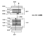
図22において、ガラス基板102とガラス基板208の板厚差の2倍が可干渉距離6μm以下の場合、光の干渉が強くなる。板厚差が可干渉距離を超えると、干渉は徐々に消失する。実際に用いるガラス基板の板厚差は可干渉距離の数倍になり、干渉の発生を防ぐことが可能となる。
式3
式4
以上から有効な副次的な光路のうち選択可能なものは上述の光路のみとなる。
[例3]表示用セルの正面側のガラス基板として、板厚が0.55mmのガラス基板を用い、背面側のガラス基板として、板厚が0.5mmのガラス基板を用いた。また、補償セルのガラス基板として板厚が0.5mmのガラス基板を用いた。そして、例1と同様に液晶表示装置を作成した。表示用セルと補償セルの隣接しあうガラス基板の板厚の差は、0.05mmである。この表示用セルの液晶層に電圧を印加しない場合、筋むらが発生しない良好な黒色表示を得ることができた。
2,8 ガラス基板
3,7 透明電極
4,6 配向膜
5 液晶層
21 補償セル
22,28 ガラス基板
24,26 配向膜
25 液晶層
31 バックライト
32 第一の偏光板
33 第二の偏光板
Claims (2)
- 透明基板の板厚分布を検査する透明基板の検査方法であって、
板厚分布の状況が既知である第一の透明基板と、検査対象となる第二の透明基板とを準備し、第一の透明基板と第二の透明基板の平均板厚の差が50μm以内であるようにし、
第一の基板と第二の基板とを光が透過し得るように、前記第一の透明基板および前記第二の透明基板を配置し、
第一の基板と第二の基板の基板間隙が0.1mm以上であるようにし、
ピーク輝度に対する半値幅が5nm以上である光を照射する光源を準備し、
前記第一の透明基板および前記第二の透明基板を通過する光の干渉強度分布によって、第二の透明基板の板厚分布の程度を判断する
ことを特徴とする透明基板の検査方法。 - 第一の透明基板と第二の透明基板を通過する光の干渉によって確認される干渉縞の本数に応じた板厚分布が第二の透明基板に生じていると判断する請求項1に記載の透明基板の検査方法。
Priority Applications (1)
| Application Number | Priority Date | Filing Date | Title |
|---|---|---|---|
| JP2008262192A JP4795414B2 (ja) | 2002-04-26 | 2008-10-08 | 透明基板の検査方法 |
Applications Claiming Priority (3)
| Application Number | Priority Date | Filing Date | Title |
|---|---|---|---|
| JP2002126916 | 2002-04-26 | ||
| JP2002126916 | 2002-04-26 | ||
| JP2008262192A JP4795414B2 (ja) | 2002-04-26 | 2008-10-08 | 透明基板の検査方法 |
Related Parent Applications (1)
| Application Number | Title | Priority Date | Filing Date |
|---|---|---|---|
| JP2003122530A Division JP4219728B2 (ja) | 2002-04-26 | 2003-04-25 | 液晶表示装置 |
Publications (2)
| Publication Number | Publication Date |
|---|---|
| JP2009080120A true JP2009080120A (ja) | 2009-04-16 |
| JP4795414B2 JP4795414B2 (ja) | 2011-10-19 |
Family
ID=29208166
Family Applications (1)
| Application Number | Title | Priority Date | Filing Date |
|---|---|---|---|
| JP2008262192A Expired - Fee Related JP4795414B2 (ja) | 2002-04-26 | 2008-10-08 | 透明基板の検査方法 |
Country Status (4)
| Country | Link |
|---|---|
| US (2) | US6906763B2 (ja) |
| EP (2) | EP1359460B1 (ja) |
| JP (1) | JP4795414B2 (ja) |
| DE (2) | DE60307522T2 (ja) |
Cited By (1)
| Publication number | Priority date | Publication date | Assignee | Title |
|---|---|---|---|---|
| KR101250126B1 (ko) | 2010-07-14 | 2013-04-03 | (주)쎄미시스코 | 복수의 기판들을 검사하는 방법 및 시스템 |
Families Citing this family (13)
| Publication number | Priority date | Publication date | Assignee | Title |
|---|---|---|---|---|
| TWI241437B (en) * | 2003-05-30 | 2005-10-11 | Toppoly Optoelectronics Corp | Dual liquid crystal display |
| WO2007010728A1 (ja) * | 2005-07-22 | 2007-01-25 | Asahi Glass Company, Limited | 液晶表示素子 |
| US20070151296A1 (en) * | 2005-12-22 | 2007-07-05 | Photon Dynamics, Inc. | Method and apparatus for handling and aligning glass substrates |
| GB0611156D0 (en) * | 2006-06-07 | 2006-07-19 | Qinetiq Ltd | Optical inspection |
| KR101280505B1 (ko) * | 2008-03-03 | 2013-07-05 | 엘지디스플레이 주식회사 | 표준 셀을 이용한 우네리 측정 장비 및 그 측정 방법 |
| WO2010011779A2 (en) * | 2008-07-23 | 2010-01-28 | Flextronics Ap, Llc | Integration design for capacitive touch panels and liquid crystal displays |
| CN102736312B (zh) * | 2012-06-15 | 2014-11-26 | 深圳市华星光电技术有限公司 | 液晶显示装置及其制造方法 |
| KR20140078299A (ko) * | 2012-12-17 | 2014-06-25 | 삼성디스플레이 주식회사 | 표시기판의 검사 장치 |
| CN107331693B (zh) * | 2017-08-31 | 2022-06-07 | 京东方科技集团股份有限公司 | 一种有机电致发光显示面板及其制备方法 |
| JP6847305B2 (ja) * | 2018-12-20 | 2021-03-24 | ベバスト エスエーWebasto SE | 液晶配列を含む複合材を有する車両用窓ガラス |
| KR20220023874A (ko) | 2020-08-20 | 2022-03-03 | 삼성디스플레이 주식회사 | 표시 장치 광학 성능 테스트용 광학 검사 기기 및 이를 이용한 광학 검사 방법 |
| CN115469472B (zh) * | 2021-06-10 | 2024-09-17 | 重庆康佳光电技术研究院有限公司 | 键合检测装置及方法 |
| CN116481431A (zh) * | 2023-04-23 | 2023-07-25 | 齐鲁工业大学(山东省科学院) | 一种微移动预警液晶传感器及其制备方法和应用 |
Citations (12)
| Publication number | Priority date | Publication date | Assignee | Title |
|---|---|---|---|---|
| JPS5265467A (en) * | 1975-11-26 | 1977-05-30 | Canon Inc | Measuring method |
| JPS6171305A (ja) * | 1984-09-14 | 1986-04-12 | Agency Of Ind Science & Technol | 膜厚測定装置 |
| JPH0861938A (ja) * | 1994-08-18 | 1996-03-08 | Dainippon Printing Co Ltd | 肉厚分布検査方法及び検査装置 |
| JPH08219729A (ja) * | 1995-02-14 | 1996-08-30 | Jeol Ltd | 膜厚測定装置 |
| JPH0961125A (ja) * | 1995-08-25 | 1997-03-07 | Fuji Photo Optical Co Ltd | 積層板検査システム |
| JPH09113927A (ja) * | 1995-10-18 | 1997-05-02 | Fujitsu Ltd | 光変調素子、その製造方法、及び、光学装置 |
| JPH11344314A (ja) * | 1998-05-29 | 1999-12-14 | Optrex Corp | 膜厚測定装置 |
| JP2000221008A (ja) * | 1999-02-02 | 2000-08-11 | Nippon Maxis:Kk | 透明基板の検査方法および透明基板の検査装置 |
| JP2001159751A (ja) * | 1999-09-24 | 2001-06-12 | Susumu Sato | 液晶セルパラメータ検出装置 |
| JP2002107119A (ja) * | 2000-07-26 | 2002-04-10 | Nippi:Kk | 被測定物の厚さ測定方法及びその装置 |
| JP2002286409A (ja) * | 2001-03-26 | 2002-10-03 | Fuji Photo Optical Co Ltd | 干渉計装置 |
| JP2004510958A (ja) * | 2000-08-08 | 2004-04-08 | ザイゴ コーポレーション | 周波数変換位相シフト干渉計測法 |
Family Cites Families (8)
| Publication number | Priority date | Publication date | Assignee | Title |
|---|---|---|---|---|
| US4523812A (en) * | 1982-11-23 | 1985-06-18 | Texas Instruments Incorporated | Plastic liquid crystal devices with unequal substrate thicknesses |
| JPS63271423A (ja) * | 1987-04-30 | 1988-11-09 | Seiko Epson Corp | 液晶表示装置 |
| CN1047003C (zh) * | 1993-09-29 | 1999-12-01 | 阿克佐诺贝尔公司 | 制造液晶显示器的方法及由该方法得到的液晶显示器 |
| US5502564A (en) * | 1994-09-13 | 1996-03-26 | Hughes Aircraft Company | Substrate thickness measurement using oblique incidence multispectral interferometry |
| JP3071658B2 (ja) * | 1994-11-02 | 2000-07-31 | シャープ株式会社 | 液晶表示素子 |
| JP3065494B2 (ja) * | 1994-12-02 | 2000-07-17 | 東芝ライテック株式会社 | 蛍光ランプおよびこれを用いたカラー液晶表示装置 |
| US5953090A (en) * | 1995-06-07 | 1999-09-14 | Asahi Glass Company Ltd. | Reflection type color liquid crystal display apparatus |
| JPH11259007A (ja) * | 1998-03-10 | 1999-09-24 | Sony Corp | 反射型表示装置 |
-
2003
- 2003-04-28 US US10/423,940 patent/US6906763B2/en not_active Expired - Lifetime
- 2003-04-28 DE DE60307522T patent/DE60307522T2/de not_active Expired - Fee Related
- 2003-04-28 EP EP03009542A patent/EP1359460B1/en not_active Expired - Lifetime
- 2003-04-28 DE DE60302698T patent/DE60302698T2/de not_active Expired - Lifetime
- 2003-04-28 EP EP05020503A patent/EP1607789B1/en not_active Expired - Lifetime
-
2005
- 2005-03-03 US US11/069,958 patent/US20050140853A1/en not_active Abandoned
-
2008
- 2008-10-08 JP JP2008262192A patent/JP4795414B2/ja not_active Expired - Fee Related
Patent Citations (12)
| Publication number | Priority date | Publication date | Assignee | Title |
|---|---|---|---|---|
| JPS5265467A (en) * | 1975-11-26 | 1977-05-30 | Canon Inc | Measuring method |
| JPS6171305A (ja) * | 1984-09-14 | 1986-04-12 | Agency Of Ind Science & Technol | 膜厚測定装置 |
| JPH0861938A (ja) * | 1994-08-18 | 1996-03-08 | Dainippon Printing Co Ltd | 肉厚分布検査方法及び検査装置 |
| JPH08219729A (ja) * | 1995-02-14 | 1996-08-30 | Jeol Ltd | 膜厚測定装置 |
| JPH0961125A (ja) * | 1995-08-25 | 1997-03-07 | Fuji Photo Optical Co Ltd | 積層板検査システム |
| JPH09113927A (ja) * | 1995-10-18 | 1997-05-02 | Fujitsu Ltd | 光変調素子、その製造方法、及び、光学装置 |
| JPH11344314A (ja) * | 1998-05-29 | 1999-12-14 | Optrex Corp | 膜厚測定装置 |
| JP2000221008A (ja) * | 1999-02-02 | 2000-08-11 | Nippon Maxis:Kk | 透明基板の検査方法および透明基板の検査装置 |
| JP2001159751A (ja) * | 1999-09-24 | 2001-06-12 | Susumu Sato | 液晶セルパラメータ検出装置 |
| JP2002107119A (ja) * | 2000-07-26 | 2002-04-10 | Nippi:Kk | 被測定物の厚さ測定方法及びその装置 |
| JP2004510958A (ja) * | 2000-08-08 | 2004-04-08 | ザイゴ コーポレーション | 周波数変換位相シフト干渉計測法 |
| JP2002286409A (ja) * | 2001-03-26 | 2002-10-03 | Fuji Photo Optical Co Ltd | 干渉計装置 |
Cited By (1)
| Publication number | Priority date | Publication date | Assignee | Title |
|---|---|---|---|---|
| KR101250126B1 (ko) | 2010-07-14 | 2013-04-03 | (주)쎄미시스코 | 복수의 기판들을 검사하는 방법 및 시스템 |
Also Published As
| Publication number | Publication date |
|---|---|
| EP1359460A2 (en) | 2003-11-05 |
| JP4795414B2 (ja) | 2011-10-19 |
| EP1607789A1 (en) | 2005-12-21 |
| US20040008297A1 (en) | 2004-01-15 |
| EP1607789B1 (en) | 2006-08-09 |
| EP1359460A3 (en) | 2004-01-14 |
| DE60307522T2 (de) | 2007-06-06 |
| US20050140853A1 (en) | 2005-06-30 |
| DE60302698D1 (de) | 2006-01-19 |
| DE60307522D1 (de) | 2006-09-21 |
| US6906763B2 (en) | 2005-06-14 |
| DE60302698T2 (de) | 2006-08-24 |
| EP1359460B1 (en) | 2005-12-14 |
Similar Documents
| Publication | Publication Date | Title |
|---|---|---|
| JP4795414B2 (ja) | 透明基板の検査方法 | |
| KR100859301B1 (ko) | 액정 표시 장치 | |
| JP3301219B2 (ja) | 液晶表示装置 | |
| KR100699375B1 (ko) | 액정 표시 장치 | |
| KR19990077709A (ko) | 반사형 표시 장치 | |
| CN107407833A (zh) | 镜面显示器 | |
| KR20010020221A (ko) | 반사형 액정 표시 장치 및 그것으로 구성되는 터치패널 일체형 반사형 액정 표시 장치 | |
| WO2010137376A1 (ja) | 液晶表示装置 | |
| US20210364844A1 (en) | Display apparatus | |
| WO2000034822A1 (fr) | Dispositif d'affichage a cristaux liquides | |
| JPH08292413A (ja) | 液晶表示装置 | |
| TW200717047A (en) | Polarizing plate having optical compensation layer, liquid crystal panel using the polarizing plate having optical compensation layer, liquid crystal display device, and image display device | |
| KR20080067041A (ko) | 반투과형 액정 표시 패널 | |
| JP2009104016A (ja) | 液晶表示装置 | |
| CN105093767A (zh) | 液晶显示设备 | |
| JP4219728B2 (ja) | 液晶表示装置 | |
| JP2019066531A (ja) | 液晶モジュール | |
| JPWO2009101746A1 (ja) | バックライトユニット及び液晶表示装置 | |
| US20160085114A1 (en) | Display device | |
| JP5636201B2 (ja) | 表示パネルまたは表示パネルを用いた表示装置 | |
| JP5274052B2 (ja) | 液晶表示装置 | |
| WO2007132608A1 (ja) | 液晶表示装置 | |
| JPWO2007010728A1 (ja) | 液晶表示素子 | |
| US20240329471A1 (en) | Marks for Angular Optical Filters | |
| US20060250553A1 (en) | Display device having a pixel unit with a transmissive area and transreflective area |
Legal Events
| Date | Code | Title | Description |
|---|---|---|---|
| A131 | Notification of reasons for refusal |
Free format text: JAPANESE INTERMEDIATE CODE: A131 Effective date: 20110517 |
|
| A521 | Written amendment |
Free format text: JAPANESE INTERMEDIATE CODE: A523 Effective date: 20110701 |
|
| TRDD | Decision of grant or rejection written | ||
| A01 | Written decision to grant a patent or to grant a registration (utility model) |
Free format text: JAPANESE INTERMEDIATE CODE: A01 Effective date: 20110726 |
|
| A01 | Written decision to grant a patent or to grant a registration (utility model) |
Free format text: JAPANESE INTERMEDIATE CODE: A01 |
|
| A61 | First payment of annual fees (during grant procedure) |
Free format text: JAPANESE INTERMEDIATE CODE: A61 Effective date: 20110727 |
|
| R150 | Certificate of patent or registration of utility model |
Ref document number: 4795414 Country of ref document: JP Free format text: JAPANESE INTERMEDIATE CODE: R150 Free format text: JAPANESE INTERMEDIATE CODE: R150 |
|
| FPAY | Renewal fee payment (event date is renewal date of database) |
Free format text: PAYMENT UNTIL: 20140805 Year of fee payment: 3 |
|
| FPAY | Renewal fee payment (event date is renewal date of database) |
Free format text: PAYMENT UNTIL: 20140805 Year of fee payment: 3 |
|
| S533 | Written request for registration of change of name |
Free format text: JAPANESE INTERMEDIATE CODE: R313533 |
|
| FPAY | Renewal fee payment (event date is renewal date of database) |
Free format text: PAYMENT UNTIL: 20140805 Year of fee payment: 3 |
|
| R350 | Written notification of registration of transfer |
Free format text: JAPANESE INTERMEDIATE CODE: R350 |
|
| R250 | Receipt of annual fees |
Free format text: JAPANESE INTERMEDIATE CODE: R250 |
|
| R250 | Receipt of annual fees |
Free format text: JAPANESE INTERMEDIATE CODE: R250 |
|
| R250 | Receipt of annual fees |
Free format text: JAPANESE INTERMEDIATE CODE: R250 |
|
| S111 | Request for change of ownership or part of ownership |
Free format text: JAPANESE INTERMEDIATE CODE: R313111 |
|
| R350 | Written notification of registration of transfer |
Free format text: JAPANESE INTERMEDIATE CODE: R350 |
|
| LAPS | Cancellation because of no payment of annual fees |