JP2009152575A - 自動基板処理システム及び方法 - Google Patents
自動基板処理システム及び方法 Download PDFInfo
- Publication number
- JP2009152575A JP2009152575A JP2008299841A JP2008299841A JP2009152575A JP 2009152575 A JP2009152575 A JP 2009152575A JP 2008299841 A JP2008299841 A JP 2008299841A JP 2008299841 A JP2008299841 A JP 2008299841A JP 2009152575 A JP2009152575 A JP 2009152575A
- Authority
- JP
- Japan
- Prior art keywords
- substrate
- chamber
- vibration
- processing
- support
- Prior art date
- Legal status (The legal status is an assumption and is not a legal conclusion. Google has not performed a legal analysis and makes no representation as to the accuracy of the status listed.)
- Pending
Links
Images








Classifications
-
- G—PHYSICS
- G05—CONTROLLING; REGULATING
- G05B—CONTROL OR REGULATING SYSTEMS IN GENERAL; FUNCTIONAL ELEMENTS OF SUCH SYSTEMS; MONITORING OR TESTING ARRANGEMENTS FOR SUCH SYSTEMS OR ELEMENTS
- G05B19/00—Program-control systems
- G05B19/02—Program-control systems electric
- G05B19/418—Total factory control, i.e. centrally controlling a plurality of machines, e.g. direct or distributed numerical control [DNC], flexible manufacturing systems [FMS], integrated manufacturing systems [IMS] or computer integrated manufacturing [CIM]
- G05B19/41815—Total factory control, i.e. centrally controlling a plurality of machines, e.g. direct or distributed numerical control [DNC], flexible manufacturing systems [FMS], integrated manufacturing systems [IMS] or computer integrated manufacturing [CIM] characterised by the cooperation between machine tools, manipulators and conveyor or other workpiece supply system, workcell
-
- G—PHYSICS
- G05—CONTROLLING; REGULATING
- G05B—CONTROL OR REGULATING SYSTEMS IN GENERAL; FUNCTIONAL ELEMENTS OF SUCH SYSTEMS; MONITORING OR TESTING ARRANGEMENTS FOR SUCH SYSTEMS OR ELEMENTS
- G05B11/00—Automatic controllers
- G05B11/01—Automatic controllers electric
-
- G—PHYSICS
- G05—CONTROLLING; REGULATING
- G05B—CONTROL OR REGULATING SYSTEMS IN GENERAL; FUNCTIONAL ELEMENTS OF SUCH SYSTEMS; MONITORING OR TESTING ARRANGEMENTS FOR SUCH SYSTEMS OR ELEMENTS
- G05B19/00—Program-control systems
- G05B19/02—Program-control systems electric
- G05B19/18—Numerical control [NC], i.e. automatically operating machines, in particular machine tools, e.g. in a manufacturing environment, so as to execute positioning, movement or co-ordinated operations by means of program data in numerical form
- G05B19/401—Numerical control [NC], i.e. automatically operating machines, in particular machine tools, e.g. in a manufacturing environment, so as to execute positioning, movement or co-ordinated operations by means of program data in numerical form characterised by control arrangements for measuring, e.g. calibration and initialisation, measuring workpiece for machining purposes
-
- G—PHYSICS
- G05—CONTROLLING; REGULATING
- G05B—CONTROL OR REGULATING SYSTEMS IN GENERAL; FUNCTIONAL ELEMENTS OF SUCH SYSTEMS; MONITORING OR TESTING ARRANGEMENTS FOR SUCH SYSTEMS OR ELEMENTS
- G05B19/00—Program-control systems
- G05B19/02—Program-control systems electric
- G05B19/18—Numerical control [NC], i.e. automatically operating machines, in particular machine tools, e.g. in a manufacturing environment, so as to execute positioning, movement or co-ordinated operations by means of program data in numerical form
- G05B19/402—Numerical control [NC], i.e. automatically operating machines, in particular machine tools, e.g. in a manufacturing environment, so as to execute positioning, movement or co-ordinated operations by means of program data in numerical form characterised by control arrangements for positioning, e.g. centring a tool relative to a hole in the workpiece, additional detection means to correct position
-
- Y—GENERAL TAGGING OF NEW TECHNOLOGICAL DEVELOPMENTS; GENERAL TAGGING OF CROSS-SECTIONAL TECHNOLOGIES SPANNING OVER SEVERAL SECTIONS OF THE IPC; TECHNICAL SUBJECTS COVERED BY FORMER USPC CROSS-REFERENCE ART COLLECTIONS [XRACs] AND DIGESTS
- Y02—TECHNOLOGIES OR APPLICATIONS FOR MITIGATION OR ADAPTATION AGAINST CLIMATE CHANGE
- Y02P—CLIMATE CHANGE MITIGATION TECHNOLOGIES IN THE PRODUCTION OR PROCESSING OF GOODS
- Y02P90/00—Enabling technologies with a potential contribution to greenhouse gas [GHG] emissions mitigation
- Y02P90/02—Total factory control, e.g. smart factories, flexible manufacturing systems [FMS] or integrated manufacturing systems [IMS]
Landscapes
- Engineering & Computer Science (AREA)
- Physics & Mathematics (AREA)
- General Physics & Mathematics (AREA)
- Automation & Control Theory (AREA)
- Manufacturing & Machinery (AREA)
- Human Computer Interaction (AREA)
- General Engineering & Computer Science (AREA)
- Quality & Reliability (AREA)
- Container, Conveyance, Adherence, Positioning, Of Wafer (AREA)
- Physical Vapour Deposition (AREA)
- Drying Of Semiconductors (AREA)
Abstract
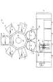
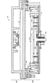
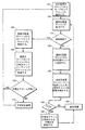
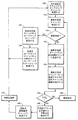
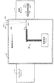
【解決手段】自動処理システムは、基板を処理するようにされた真空チャンバ18と、チャンバ内に置かれ、基板が処理されている間にチャンバ内で移動するようにされ、基板を支持するようにされた基板支持部と、基板支持部に隣接するピンと、基板が処理されている間にチャンバの中での物理的状態の変化を検出するようにされた検出器であって、ピンに結合されると共に前記支持体が移動するときに前記ピンの振動を検出するようにされた振動検出器と、前記ピンの検出された前記振動から背景振動を表すノイズ信号をフィルタするようにされたノイズフィルタとを有する検出器とを含んでいる。
【選択図】図1A
Description
Claims (10)
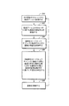
- 処理用の真空チャンバに基板を転送するステップと、
前記基板が前記チャンバ内にある間に前記基板を支持するようにされた支持部を移動させるステップを有する、前記基板を処理するステップと、
前記支持部が移動するときにピンの振動を検出するステップと、前記ピンの検出された前記振動から背景振動を表すノイズ信号をフィルタするステップとを有する、前記基板を処理する間に前記チャンバで物理的状態の変化を検出するステップと、
を含む基板処理方法。 - 前記支持部が移動するときに検出されてフィルタされた前記振動が第1のしきい値を超えた場合、第1の警報が作動するステップをさらに含む請求項1に記載の基板処理方法。
- 前記第1の警報の作動に応じて、前記基板の損傷を避けるために前記基板を処理するステップを終了するステップをさらに含む請求項2に記載の基板処理方法。
- 前記支持部が移動するときに検出されてフィルタされた前記振動が前記第1のしきい値よりも低い第2のしきい値を超えた場合、第2の警報が作動するステップを含み、前記第2の警報の作動に関わらず、前記基板を処理するステップを完了させる請求項2に記載の基板処理方法。
- 前記チャンバで物理的状態の変化を検出するステップが、前記支持部が移動するときに複数のピンの振動を検出するステップと、前記ピンの検出された前記振動からノイズ振動をフィルタするステップを有する請求項1に記載の基板処理方法。
- 基板を処理するようにされた真空チャンバと、
前記チャンバ内に置かれ、基板が処理されている間に前記チャンバ内で移動するようにされ、基板を支持するようにされた基板支持部と、
前記基板支持部に隣接するピンと、
基板が処理されている間に前記チャンバの中での物理的状態の変化を検出するようにされた検出器であって、前記ピンに結合されると共に前記支持体が移動するときに前記ピンの振動を検出するようにされた振動検出器と、前記ピンの検出された前記振動から背景振動を表すノイズ信号をフィルタするようにされたノイズフィルタとを有する検出器と、
を含むシステム。 - 前記検出器に結合され、前記支持部が移動するときに検出されてフィルタされた前記振動が第1のしきい値を超えた場合、第1の警報を作動させる警報装置をさらに含む請求項6に記載のシステム。
- 作動した前記第1の警報に応じて、前記基板の損傷を避けるために前記基板の処理を終了するようにされたコントローラをさらに含む請求項7に記載のシステム。
- 前記警報装置は、前記支持部が移動するときに検出されてフィルタされた前記振動が前記第1のしきい値よりも低い第2のしきい値を超えた場合、第2の警報が作動するようにされると共に、前記システムは、作動した前記第2の警報に関わらず、前記基板の処理を完了させるようにされたコントローラをさらに含む請求項7に記載のシステム。
- 前記基板支持部に隣接する複数のピンをさらに含み、前記振動検出器は前記支持部が移動するときに前記複数のピンの振動を検出するようにされると共に、前記ノイズフィルタは前記ピンの検出された前記振動から背景振動を表すノイズ信号をフィルタするようにされた請求項6に記載のシステム。
Applications Claiming Priority (1)
| Application Number | Priority Date | Filing Date | Title |
|---|---|---|---|
| US08/949,207 US6205870B1 (en) | 1997-10-10 | 1997-10-10 | Automated substrate processing systems and methods |
Related Parent Applications (1)
| Application Number | Title | Priority Date | Filing Date |
|---|---|---|---|
| JP2000516264A Division JP4469492B2 (ja) | 1997-10-10 | 1998-10-06 | 自動基板処理システム及び方法 |
Publications (1)
| Publication Number | Publication Date |
|---|---|
| JP2009152575A true JP2009152575A (ja) | 2009-07-09 |
Family
ID=25488747
Family Applications (2)
| Application Number | Title | Priority Date | Filing Date |
|---|---|---|---|
| JP2000516264A Expired - Fee Related JP4469492B2 (ja) | 1997-10-10 | 1998-10-06 | 自動基板処理システム及び方法 |
| JP2008299841A Pending JP2009152575A (ja) | 1997-10-10 | 2008-11-25 | 自動基板処理システム及び方法 |
Family Applications Before (1)
| Application Number | Title | Priority Date | Filing Date |
|---|---|---|---|
| JP2000516264A Expired - Fee Related JP4469492B2 (ja) | 1997-10-10 | 1998-10-06 | 自動基板処理システム及び方法 |
Country Status (5)
| Country | Link |
|---|---|
| US (2) | US6205870B1 (ja) |
| EP (1) | EP1023645A4 (ja) |
| JP (2) | JP4469492B2 (ja) |
| KR (1) | KR100638407B1 (ja) |
| WO (1) | WO1999019777A1 (ja) |
Cited By (3)
| Publication number | Priority date | Publication date | Assignee | Title |
|---|---|---|---|---|
| JP2016139737A (ja) * | 2015-01-28 | 2016-08-04 | 東京エレクトロン株式会社 | 基板処理装置 |
| JP2020087980A (ja) * | 2018-11-15 | 2020-06-04 | 川崎重工業株式会社 | ロボットシステム及びその運転方法 |
| JP2025095849A (ja) * | 2023-12-15 | 2025-06-26 | 株式会社Screenホールディングス | 減圧乾燥装置 |
Families Citing this family (33)
| Publication number | Priority date | Publication date | Assignee | Title |
|---|---|---|---|---|
| JP2001127136A (ja) * | 1999-10-29 | 2001-05-11 | Applied Materials Inc | 基板搬送ロボットの検査装置 |
| JP4856308B2 (ja) * | 2000-12-27 | 2012-01-18 | キヤノンアネルバ株式会社 | 基板処理装置及び経由チャンバー |
| JP2002203885A (ja) * | 2000-12-27 | 2002-07-19 | Anelva Corp | インターバック型基板処理装置 |
| DE60238752D1 (de) * | 2001-03-29 | 2011-02-10 | Toyota Chuo Kenkyusho Kk | Ein verfahren zum erzeugen einer hohlen struktur aus einer silizium-struktur |
| KR100914199B1 (ko) * | 2002-12-27 | 2009-08-27 | 엘지디스플레이 주식회사 | 액정표시소자를 형성하기 위한 플라즈마 증착장비 |
| US7505832B2 (en) * | 2003-05-12 | 2009-03-17 | Applied Materials, Inc. | Method and apparatus for determining a substrate exchange position in a processing system |
| US7458763B2 (en) | 2003-11-10 | 2008-12-02 | Blueshift Technologies, Inc. | Mid-entry load lock for semiconductor handling system |
| US20070269297A1 (en) | 2003-11-10 | 2007-11-22 | Meulen Peter V D | Semiconductor wafer handling and transport |
| US10086511B2 (en) | 2003-11-10 | 2018-10-02 | Brooks Automation, Inc. | Semiconductor manufacturing systems |
| US20050113976A1 (en) * | 2003-11-10 | 2005-05-26 | Blueshift Technologies, Inc. | Software controller for handling system |
| JP2005262367A (ja) * | 2004-03-18 | 2005-09-29 | Tokyo Electron Ltd | 搬送ロボットの搬送ズレ確認方法及び処理装置 |
| US20050223993A1 (en) * | 2004-04-08 | 2005-10-13 | Blomiley Eric R | Deposition apparatuses; methods for assessing alignments of substrates within deposition apparatuses; and methods for assessing thicknesses of deposited layers within deposition apparatuses |
| EP1790160A4 (en) * | 2004-09-15 | 2009-08-26 | Nokia Corp | PROVIDING CHANNEL JUMPING FLOWS TO PROGRAM RECEIVERS |
| JP4006004B2 (ja) * | 2004-12-28 | 2007-11-14 | 株式会社東芝 | 半導体製造装置及び半導体装置の製造方法 |
| US7522267B2 (en) * | 2005-07-11 | 2009-04-21 | Brooks Automation, Inc. | Substrate transport apparatus with automated alignment |
| US7644637B2 (en) * | 2006-09-25 | 2010-01-12 | Omniprobe, Inc. | Method and apparatus for transfer of samples in a controlled environment |
| US7712370B2 (en) * | 2006-12-22 | 2010-05-11 | Asm Japan K.K. | Method of detecting occurrence of sticking of substrate |
| US8758514B2 (en) | 2007-03-02 | 2014-06-24 | Asm Japan K.K. | Cluster type semiconductor processing apparatus |
| JP5597536B2 (ja) * | 2008-08-01 | 2014-10-01 | 株式会社アルバック | 搬送ロボットのティーチング方法 |
| JP5261085B2 (ja) * | 2008-09-05 | 2013-08-14 | 東京エレクトロン株式会社 | 基板載置機構、基板処理装置、基板載置機構の制御方法及び記憶媒体 |
| US20100129940A1 (en) * | 2008-11-24 | 2010-05-27 | Texas Instruments Incorporated | Vibration monitoring of electronic substrate handling systems |
| US20100151127A1 (en) * | 2008-12-12 | 2010-06-17 | Applied Materials, Inc. | Apparatus and method for preventing process system contamination |
| JP5303254B2 (ja) * | 2008-12-15 | 2013-10-02 | 東京エレクトロン株式会社 | 異物除去方法及び記憶媒体 |
| US9691650B2 (en) * | 2009-09-29 | 2017-06-27 | Applied Materials, Inc. | Substrate transfer robot with chamber and substrate monitoring capability |
| JP5723612B2 (ja) * | 2011-01-28 | 2015-05-27 | リンテック株式会社 | 板状部材の支持装置 |
| US9371584B2 (en) * | 2011-03-09 | 2016-06-21 | Applied Materials, Inc. | Processing chamber and method for centering a substrate therein |
| US20130156530A1 (en) * | 2011-12-14 | 2013-06-20 | Intermolecular, Inc. | Method and apparatus for reducing contamination of substrate |
| JP6114060B2 (ja) * | 2013-02-27 | 2017-04-12 | 東京エレクトロン株式会社 | 基板搬送装置、基板受渡位置確認方法及び基板処理システム |
| US9857780B1 (en) * | 2013-03-15 | 2018-01-02 | Daniel Reed | Positioning work stop |
| US10002781B2 (en) | 2014-11-10 | 2018-06-19 | Brooks Automation, Inc. | Tool auto-teach method and apparatus |
| JP7335647B2 (ja) * | 2018-08-10 | 2023-08-30 | アピックヤマダ株式会社 | ワーク搬送装置及び樹脂モールド装置 |
| DE102018009871A1 (de) * | 2018-12-19 | 2020-06-25 | Vat Holding Ag | Stifthubvorrichtung mit Zustandsüberwachung |
| CN115642107A (zh) * | 2022-10-20 | 2023-01-24 | 拓荆科技股份有限公司 | 一种加热盘对中调节装置及调节方法 |
Citations (4)
| Publication number | Priority date | Publication date | Assignee | Title |
|---|---|---|---|---|
| JPH04193951A (ja) * | 1990-11-28 | 1992-07-14 | Tokyo Electron Ltd | 保持装置 |
| JPH05315433A (ja) * | 1992-05-14 | 1993-11-26 | Nec Corp | ウェハホルダ |
| JPH06340975A (ja) * | 1993-01-28 | 1994-12-13 | Applied Materials Inc | 加熱された支持部上のシャドーフレーム及び大型平面基板の整列 |
| JPH09186226A (ja) * | 1995-11-29 | 1997-07-15 | Applied Materials Inc | 半導体ウェーハ・アライメント部材及びクランプ・リング |
Family Cites Families (50)
| Publication number | Priority date | Publication date | Assignee | Title |
|---|---|---|---|---|
| US4158171A (en) | 1977-09-14 | 1979-06-12 | Ade Corporation | Wafer edge detection system |
| US4344160A (en) | 1980-05-02 | 1982-08-10 | The Perkin-Elmer Corporation | Automatic wafer focusing and flattening system |
| IT1200370B (it) * | 1981-03-25 | 1989-01-18 | Goldstein Pinchas | Apparecchiatura di protezione ottica a traguardo passiva e complesso riflettore stabilizzato impiegato in essa |
| US4457664A (en) | 1982-03-22 | 1984-07-03 | Ade Corporation | Wafer alignment station |
| US4409087A (en) | 1982-05-18 | 1983-10-11 | The Perkin-Elmer Corp. | Wafer detection circuitry for high vacuum use |
| US4513430A (en) | 1982-05-24 | 1985-04-23 | Varian Associates, Inc. | Missing or broken wafer sensor |
| US4603466A (en) | 1984-02-17 | 1986-08-05 | Gca Corporation | Wafer chuck |
| US4657621A (en) | 1984-10-22 | 1987-04-14 | Texas Instruments Incorporated | Low particulate vacuum chamber input/output valve |
| US4873447A (en) * | 1985-01-28 | 1989-10-10 | Tokyo Electron Limited | Wafer transport apparatus for ion implantation apparatus |
| US4836733A (en) | 1986-04-28 | 1989-06-06 | Varian Associates, Inc. | Wafer transfer system |
| US4770590A (en) | 1986-05-16 | 1988-09-13 | Silicon Valley Group, Inc. | Method and apparatus for transferring wafers between cassettes and a boat |
| US4697089A (en) | 1986-06-18 | 1987-09-29 | Tegal Corporation | Dual wavelength sensor which employs object as part of a corner reflector |
| JPH0652758B2 (ja) | 1987-02-09 | 1994-07-06 | 日本電信電話株式会社 | 静電チヤツク |
| US4819167A (en) | 1987-04-20 | 1989-04-04 | Applied Materials, Inc. | System and method for detecting the center of an integrated circuit wafer |
| JP2678381B2 (ja) | 1987-05-06 | 1997-11-17 | ユニサーチ・リミテッド | 交流電界励振を利用した静電チャック |
| KR960010067B1 (ko) | 1987-08-07 | 1996-07-25 | 도오교오 에레구토론 가부시끼가이샤 | 회전 이동 장치 |
| US5102280A (en) | 1989-03-07 | 1992-04-07 | Ade Corporation | Robot prealigner |
| JP2779950B2 (ja) | 1989-04-25 | 1998-07-23 | 東陶機器株式会社 | 静電チャックの電圧印加方法および電圧印加装置 |
| JP2865320B2 (ja) | 1989-08-07 | 1999-03-08 | 株式会社資生堂 | 固型化粧料組成物 |
| JPH0736417B2 (ja) | 1989-10-24 | 1995-04-19 | 株式会社メツクス | ウエハーの位置決め装置 |
| US5194743A (en) | 1990-04-06 | 1993-03-16 | Nikon Corporation | Device for positioning circular semiconductor wafers |
| US5281921A (en) | 1990-04-24 | 1994-01-25 | Novak James L | Non-contact capacitance based image sensing method and system |
| US5208648A (en) | 1991-03-11 | 1993-05-04 | International Business Machines Corporation | Apparatus and a method for high numerical aperture microscopic examination of materials |
| US5325261A (en) | 1991-05-17 | 1994-06-28 | Unisearch Limited | Electrostatic chuck with improved release |
| KR100188454B1 (ko) * | 1991-05-28 | 1999-06-01 | 이노우에 아키라 | 기판 처리 장치 |
| US5319216A (en) | 1991-07-26 | 1994-06-07 | Tokyo Electron Limited | Substrate detector with light emitting and receiving elements arranged in staggered fashion and a polarization filter |
| US5275683A (en) | 1991-10-24 | 1994-01-04 | Tokyo Electron Limited | Mount for supporting substrates and plasma processing apparatus using the same |
| JP3074579B2 (ja) * | 1992-01-31 | 2000-08-07 | キヤノン株式会社 | 位置ずれ補正方法 |
| US5222329A (en) | 1992-03-26 | 1993-06-29 | Micron Technology, Inc. | Acoustical method and system for detecting and controlling chemical-mechanical polishing (CMP) depths into layers of conductors, semiconductors, and dielectric materials |
| EP0597637B1 (en) * | 1992-11-12 | 2000-08-23 | Applied Materials, Inc. | System and method for automated positioning of a substrate in a processing chamber |
| JPH06156624A (ja) | 1992-11-13 | 1994-06-03 | Ebara Corp | 載置物の置き台 |
| KR100238629B1 (ko) | 1992-12-17 | 2000-01-15 | 히가시 데쓰로 | 정전척을 가지는 재치대 및 이것을 이용한 플라즈마 처리장치 |
| US5436790A (en) | 1993-01-15 | 1995-07-25 | Eaton Corporation | Wafer sensing and clamping monitor |
| JP2683208B2 (ja) | 1993-01-28 | 1997-11-26 | アプライド マテリアルズ インコーポレイテッド | ロボット機構を用いた搬入および搬出のためのワークピース位置合わせ方法および装置 |
| US5535306A (en) | 1993-01-28 | 1996-07-09 | Applied Materials Inc. | Self-calibration system for robot mechanisms |
| JPH06244268A (ja) | 1993-02-16 | 1994-09-02 | Tokyo Electron Tohoku Ltd | 移載装置 |
| US5539323A (en) | 1993-05-07 | 1996-07-23 | Brooks Automation, Inc. | Sensor for articles such as wafers on end effector |
| EP0634787B1 (en) | 1993-07-15 | 1997-05-02 | Applied Materials, Inc. | Subsrate tray and ceramic blade for semiconductor processing apparatus |
| JP3297771B2 (ja) | 1993-11-05 | 2002-07-02 | ソニー株式会社 | 半導体製造装置 |
| JPH07249586A (ja) | 1993-12-22 | 1995-09-26 | Tokyo Electron Ltd | 処理装置及びその製造方法並びに被処理体の処理方法 |
| US5441768A (en) | 1994-02-08 | 1995-08-15 | Applied Materials, Inc. | Multi-step chemical vapor deposition method for thin film transistors |
| US5466945A (en) * | 1994-03-23 | 1995-11-14 | Eaton Corporation | Apparatus for detecting proper positioning of objects in a holder |
| US5563798A (en) * | 1994-04-05 | 1996-10-08 | Applied Materials, Inc. | Wafer positioning system |
| US5518593A (en) | 1994-04-29 | 1996-05-21 | Applied Komatsu Technology, Inc. | Shield configuration for vacuum chamber |
| US5606251A (en) | 1994-07-15 | 1997-02-25 | Ontrak Systems, Inc. | Method and apparatus for detecting a substrate in a substrate processing system |
| US5654508A (en) | 1995-02-23 | 1997-08-05 | Gibbs; John Harvey | Method of determining a store's physical inventory |
| JP3973112B2 (ja) * | 1995-06-07 | 2007-09-12 | バリアン・セミコンダクター・エクイップメント・アソシエイツ・インコーポレイテッド | ウェーハの向き整合システム |
| US5607602A (en) | 1995-06-07 | 1997-03-04 | Applied Komatsu Technology, Inc. | High-rate dry-etch of indium and tin oxides by hydrogen and halogen radicals such as derived from HCl gas |
| US5768125A (en) * | 1995-12-08 | 1998-06-16 | Asm International N.V. | Apparatus for transferring a substantially circular article |
| US5948986A (en) | 1997-12-26 | 1999-09-07 | Applied Materials, Inc. | Monitoring of wafer presence and position in semiconductor processing operations |
-
1997
- 1997-10-10 US US08/949,207 patent/US6205870B1/en not_active Expired - Lifetime
-
1998
- 1998-10-06 KR KR1020007003884A patent/KR100638407B1/ko not_active Expired - Fee Related
- 1998-10-06 EP EP98949782A patent/EP1023645A4/en not_active Withdrawn
- 1998-10-06 JP JP2000516264A patent/JP4469492B2/ja not_active Expired - Fee Related
- 1998-10-06 WO PCT/US1998/020999 patent/WO1999019777A1/en not_active Ceased
-
1999
- 1999-09-08 US US09/392,110 patent/US6257045B1/en not_active Expired - Lifetime
-
2008
- 2008-11-25 JP JP2008299841A patent/JP2009152575A/ja active Pending
Patent Citations (4)
| Publication number | Priority date | Publication date | Assignee | Title |
|---|---|---|---|---|
| JPH04193951A (ja) * | 1990-11-28 | 1992-07-14 | Tokyo Electron Ltd | 保持装置 |
| JPH05315433A (ja) * | 1992-05-14 | 1993-11-26 | Nec Corp | ウェハホルダ |
| JPH06340975A (ja) * | 1993-01-28 | 1994-12-13 | Applied Materials Inc | 加熱された支持部上のシャドーフレーム及び大型平面基板の整列 |
| JPH09186226A (ja) * | 1995-11-29 | 1997-07-15 | Applied Materials Inc | 半導体ウェーハ・アライメント部材及びクランプ・リング |
Cited By (5)
| Publication number | Priority date | Publication date | Assignee | Title |
|---|---|---|---|---|
| JP2016139737A (ja) * | 2015-01-28 | 2016-08-04 | 東京エレクトロン株式会社 | 基板処理装置 |
| JP2020087980A (ja) * | 2018-11-15 | 2020-06-04 | 川崎重工業株式会社 | ロボットシステム及びその運転方法 |
| JP7149815B2 (ja) | 2018-11-15 | 2022-10-07 | 川崎重工業株式会社 | ロボットシステム及びその運転方法 |
| JP2025095849A (ja) * | 2023-12-15 | 2025-06-26 | 株式会社Screenホールディングス | 減圧乾燥装置 |
| JP7771155B2 (ja) | 2023-12-15 | 2025-11-17 | 株式会社Screenホールディングス | 減圧乾燥装置 |
Also Published As
| Publication number | Publication date |
|---|---|
| US6257045B1 (en) | 2001-07-10 |
| WO1999019777A1 (en) | 1999-04-22 |
| US6205870B1 (en) | 2001-03-27 |
| KR100638407B1 (ko) | 2006-10-24 |
| WO1999019777A8 (en) | 1999-10-28 |
| KR20010031055A (ko) | 2001-04-16 |
| WO1999019777A9 (en) | 1999-11-25 |
| EP1023645A4 (en) | 2004-12-22 |
| JP2003526894A (ja) | 2003-09-09 |
| EP1023645A1 (en) | 2000-08-02 |
| JP4469492B2 (ja) | 2010-05-26 |
Similar Documents
| Publication | Publication Date | Title |
|---|---|---|
| JP4469492B2 (ja) | 自動基板処理システム及び方法 | |
| US6827825B2 (en) | Method for detecting the position of a shutter disk in a physical vapor deposition chamber | |
| CN110504190A (zh) | 输送方法和输送装置 | |
| JP4222997B2 (ja) | 基板処理装置 | |
| US20040182698A1 (en) | Shutter disk and blade for physical vapor deposition chamber | |
| KR101430505B1 (ko) | 진공 성막 장치 및 진공 성막 장치의 셔터판 위치 검출 방법 | |
| US20100119349A1 (en) | Substrate alignment system | |
| US6944517B2 (en) | Substrate apparatus calibration and synchronization procedure | |
| WO2009135066A2 (en) | End effector to substrate offset detection and correction | |
| JPH0533010Y2 (ja) | ||
| JP2003273190A (ja) | 真空処理装置、ゲ−トバルブ、および欠落被搬送体の検出方法 | |
| US7255524B2 (en) | Substrate cassette mapper | |
| JPH07260455A (ja) | 基板位置決め方法及び装置 | |
| JPH10313037A (ja) | 基板搬送システムの監視装置 | |
| JPH11150078A (ja) | 縦型熱処理炉 | |
| JP3674063B2 (ja) | ウェハ搬送装置 | |
| JP3295915B2 (ja) | 半導体ウエファの位置決め方法とその装置 | |
| KR102777032B1 (ko) | 기판 처리 장치 | |
| TW202314949A (zh) | 處理擋板裝置 | |
| JP2921880B2 (ja) | 微粒子モニタ付き半導体製造装置 | |
| JP2000349134A (ja) | 処理装置 | |
| CN120174323A (zh) | 晶圆出片的纠偏装置、纠偏方法和薄膜沉积设备 | |
| KR100598251B1 (ko) | 웨이퍼 로딩 시스템 | |
| JP2001217303A (ja) | ガラス基板の基板端検出装置 | |
| JP2003031643A (ja) | 基板処理装置 |
Legal Events
| Date | Code | Title | Description |
|---|---|---|---|
| A977 | Report on retrieval |
Free format text: JAPANESE INTERMEDIATE CODE: A971007 Effective date: 20100901 |
|
| A711 | Notification of change in applicant |
Free format text: JAPANESE INTERMEDIATE CODE: A711 Effective date: 20101129 |
|
| RD03 | Notification of appointment of power of attorney |
Free format text: JAPANESE INTERMEDIATE CODE: A7423 Effective date: 20101227 |
|
| A521 | Written amendment |
Free format text: JAPANESE INTERMEDIATE CODE: A523 Effective date: 20110127 |
|
| RD04 | Notification of resignation of power of attorney |
Free format text: JAPANESE INTERMEDIATE CODE: A7424 Effective date: 20110317 |
|
| RD04 | Notification of resignation of power of attorney |
Free format text: JAPANESE INTERMEDIATE CODE: A7424 Effective date: 20110318 |
|
| A131 | Notification of reasons for refusal |
Free format text: JAPANESE INTERMEDIATE CODE: A131 Effective date: 20110705 |
|
| A521 | Written amendment |
Free format text: JAPANESE INTERMEDIATE CODE: A523 Effective date: 20110901 |
|
| A131 | Notification of reasons for refusal |
Free format text: JAPANESE INTERMEDIATE CODE: A131 Effective date: 20120207 |
|
| A02 | Decision of refusal |
Free format text: JAPANESE INTERMEDIATE CODE: A02 Effective date: 20120605 |