JP2009169089A - 光偏向器 - Google Patents
光偏向器 Download PDFInfo
- Publication number
- JP2009169089A JP2009169089A JP2008006950A JP2008006950A JP2009169089A JP 2009169089 A JP2009169089 A JP 2009169089A JP 2008006950 A JP2008006950 A JP 2008006950A JP 2008006950 A JP2008006950 A JP 2008006950A JP 2009169089 A JP2009169089 A JP 2009169089A
- Authority
- JP
- Japan
- Prior art keywords
- optical deflector
- piezoelectric
- mirror
- pair
- movable frame
- Prior art date
- Legal status (The legal status is an assumption and is not a legal conclusion. Google has not performed a legal analysis and makes no representation as to the accuracy of the status listed.)
- Granted
Links
Images


Classifications
-
- G—PHYSICS
- G02—OPTICS
- G02B—OPTICAL ELEMENTS, SYSTEMS OR APPARATUS
- G02B26/00—Optical devices or arrangements for the control of light using movable or deformable optical elements
- G02B26/08—Optical devices or arrangements for the control of light using movable or deformable optical elements for controlling the direction of light
- G02B26/10—Scanning systems
- G02B26/105—Scanning systems with one or more pivoting mirrors or galvano-mirrors
-
- B—PERFORMING OPERATIONS; TRANSPORTING
- B81—MICROSTRUCTURAL TECHNOLOGY
- B81B—MICROSTRUCTURAL DEVICES OR SYSTEMS, e.g. MICROMECHANICAL DEVICES
- B81B3/00—Devices comprising flexible or deformable elements, e.g. comprising elastic tongues or membranes
- B81B3/0035—Constitution or structural means for controlling the movement of the flexible or deformable elements
- B81B3/0051—For defining the movement, i.e. structures that guide or limit the movement of an element
-
- B—PERFORMING OPERATIONS; TRANSPORTING
- B81—MICROSTRUCTURAL TECHNOLOGY
- B81B—MICROSTRUCTURAL DEVICES OR SYSTEMS, e.g. MICROMECHANICAL DEVICES
- B81B7/00—Microstructural systems ; Auxiliary parts of microstructural devices or systems
- B81B7/0009—Structural features, others than packages, for protecting a device against environmental influences
- B81B7/0016—Protection against shocks or vibrations, e.g. vibration damping
-
- G—PHYSICS
- G02—OPTICS
- G02B—OPTICAL ELEMENTS, SYSTEMS OR APPARATUS
- G02B26/00—Optical devices or arrangements for the control of light using movable or deformable optical elements
- G02B26/08—Optical devices or arrangements for the control of light using movable or deformable optical elements for controlling the direction of light
- G02B26/0816—Optical devices or arrangements for the control of light using movable or deformable optical elements for controlling the direction of light by means of one or more reflecting elements
- G02B26/0833—Optical devices or arrangements for the control of light using movable or deformable optical elements for controlling the direction of light by means of one or more reflecting elements the reflecting element being a micromechanical device, e.g. a MEMS mirror, DMD
- G02B26/0858—Optical devices or arrangements for the control of light using movable or deformable optical elements for controlling the direction of light by means of one or more reflecting elements the reflecting element being a micromechanical device, e.g. a MEMS mirror, DMD the reflecting means being moved or deformed by piezoelectric means
Landscapes
- Physics & Mathematics (AREA)
- General Physics & Mathematics (AREA)
- Optics & Photonics (AREA)
- Engineering & Computer Science (AREA)
- Computer Hardware Design (AREA)
- Microelectronics & Electronic Packaging (AREA)
- Health & Medical Sciences (AREA)
- General Health & Medical Sciences (AREA)
- Toxicology (AREA)
- Micromachines (AREA)
- Mechanical Optical Scanning Systems (AREA)
- Mechanical Light Control Or Optical Switches (AREA)
Abstract
【解決手段】光偏向器A1は、反射面を有するミラー部1と、トーションバー2a,2bに一端が連結され他端が支持部10に連結されて支持された圧電アクチュエータ8a〜8dとを備え、圧電アクチュエータ8a〜8dに駆動電圧を印加することで、トーションバー2a,2bを介してミラー部1を回転駆動させる。光偏向器A1は、ミラー部1と支持部10との間に設けられた空隙10’に、支持部1のミラー部1に対向する部分に連結された衝撃緩和部9a,9bを有する。
【選択図】図1
Description
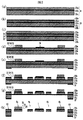
本発明の第1実施形態について、図1〜図2を参照して説明する。図1は、本実施形態における光偏向器A1の外観図、図2は、図1の光偏向器A1の製造工程を示す説明図である。
[製造工程]
図2には、光偏向器A1の製造工程を示す。なお、図2(a)〜(h)は、光偏向器A1の断面を模式的に示している。
[実施例1]
実施例1として、本実施形態の光偏向器A1の駆動特性の試験について説明する。本実施例では、上述の光偏向器A1を、共振周波数が5[kHz]となるように設計し、上述の製造工程で作製した。このとき、SOI基板の各層の厚みは、活性層30[μm]、中間酸化膜層2[μm]、ハンドリング層525[μm]とし、熱酸化シリコン膜の厚みは500[nm]とした。また、下部電極層(Ti/Pt)の厚みはTiを50[μm]、Ptを150[nm]とし、圧電体層の厚みは3[μm]とし、上部電極層(Pt)の厚みは150[nm]とした。
[比較例1]
比較例1として、衝撃緩和部9a,9bを備えない点以外は実施例1と同じ構成の光偏向器を作製した。この光偏向器に、実施例1と同様の加速度1500[G]の衝撃を付加したところ、トーションバー2a,2bが破損した。また、この光偏向器に、実施例1と同様の加速度500[G]の振動を付加したところ、トーションバー2a,2bにクラックが入り、光偏向器の機械的な特性が大幅に劣化した。
[第2実施形態]
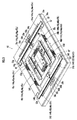
本発明の第2実施形態について、図3を参照して説明する。図3は、本発明の第2実施形態における光偏向器の構成を示す斜視図である。本実施形態の光偏向器A2は、第1実施形態のミラー部、トーションバー、2対の圧電アクチュエータを一体的に回転させるための、さらに2対の圧電アクチュエータを備えたものである。
[実施例2]
実施例2として、本実施形態の光偏向器A2の駆動特性の試験について説明する。本実施例では、上述の光偏向器A2を、ミラー部41の共振周波数が16[kHz]以上、可動枠49の共振周波数が60[Hz]となるように設計し、実施例1と同様の製造工程で作製した。
[比較例2]
比較例2として、衝撃緩和部を備えない点以外は実施例2と同じ構成の光偏向器を作製した。この光偏向器に、実施例2と同様に衝撃を付加したところ、加速度100[G]以下の衝撃に対して第2のトーションバーが破損した。
[第3実施形態]
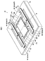
本発明の第3実施形態について、図4を参照して説明する。図4は、本発明の第3実施形態における光偏向器A3の構成を示す斜視図である。本実施形態の光偏向器A3は、衝撃緩和部のみが第1実施形態と相違する。第1実施形態と同じ構成は、同じ符号を付して説明を省略する。
[実施例3]
実施例3として、本実施形態の光偏向器A3の駆動特性の試験について説明する。本実施例では、衝撃緩和部61a,61b以外は実施例1と同様の光偏向器を作製した。衝撃緩和部61a,61bの材料としてはエポキシ樹脂系の圧膜レジストSU−8(化薬マイクロケム(株)製)を使用した。また、キュア温度は250[℃]とした。この光偏向器について、実施例1と同様に駆動信号を印加して、実施例1と同様に光偏向器の最大偏向角として±10°が得られた。
[第4実施形態]
本発明の第4実施形態について、図5を参照して説明する。図5は、本発明の第4実施形態における光偏向器A4の構成を示す斜視図である。本実施形態の光偏向器A4は、ミラー部に突起部を設けたことのみが第3実施形態と相違する。第3実施形態と同じ構成は、同じ符号を付して説明を省略する。
[実施例4]
実施例4として、本実施形態の光偏向器A4の駆動特性の試験について説明する。本実施例では、ミラー部1に突起部62a〜62fを設けた以外は実施例3と同様の光偏向器を作製した。この光偏向器について、実施例1と同様に駆動信号を印加して、実施例1と同様に光偏向器の最大偏向角として±10°が得られた。
31…SOI基板、31a…活性層、31b…中間酸化膜層、31c…ハンドリング層、32a,32b…熱酸化シリコン膜、33…下部電極層、34…圧電体層、35…上部電極層、37…Al薄膜、
41…ミラー部、41a…ミラー部支持体、41b…ミラー面反射膜、42a,42b…第1のトーションバー、44a〜44h…支持体、45a〜45h…下部電極、46a〜46h…圧電体、47a〜47h…上部電極、48a〜48d…第1の圧電アクチュエータ、49…可動枠、50a,50b…第2のトーションバー、51a〜51d…第2の圧電アクチュエータ、52…支持部、53a〜53h…上部電極パッド、54a〜54h…下部電極パッド、
61a,61b…衝撃緩和部、62a〜62f…突起部。
Claims (11)
- 反射面を有するミラー部と、該ミラー部の端部から外側に延びたトーションバーと、該ミラー部を囲むように設けられた支持部と、一端が該トーションバーに連結され他端が該支持部に連結されて支持された圧電アクチュエータとを備え、該圧電アクチュエータは、支持体上に形成された圧電体に駆動電圧を印加することで圧電駆動により屈曲変形を行う1つ以上の圧電カンチレバーを含み、該圧電アクチュエータに駆動電圧を印加することで該トーションバーを介して該ミラー部を回転駆動させる光偏向器において、
前記ミラー部と前記支持部との間に設けた空隙に、前記支持部に連結された衝撃緩和部を備えたことを特徴とする光偏向器。 - 請求項1記載の光偏向器において、前記衝撃緩和部はバネ特性を有する形状で、半導体基板を形状加工して前記支持部と一体的に形成されることを特徴とする光偏向器。
- 請求項1記載の光偏向器において、前記衝撃緩和部は、弾性を有する感光性の高分子材料をフォトリソグラフィ処理によりパターニング加工して形成されることを特徴とする光偏向器。
- 請求項3記載の光偏向器において、前記ミラー部の前記空隙側に、前記衝撃緩和部に対向するように、該ミラー部の回転駆動を妨げない所定サイズの少なくとも1つ以上の突起部が形成されることを特徴とする光偏向器。
- 請求項1〜4のいずれか記載の光偏向器において、前記圧電アクチュエータは、前記ミラー部と該ミラー部の両端から外側に延びた1対のトーションバーとを挟んで対向するように1対又は2対配置され、各圧電アクチュエータの少なくとも一端が該1対のトーションバーに連結され、他端は前記支持部に連結されて支持され、該ミラー部は、該1対又は2対の圧電アクチュエータにより回転駆動されることを特徴とする光偏向器。
- 請求項1〜4のいずれか記載の光偏向器において、前記圧電アクチュエータは、前記ミラー部と該ミラー部の両端から外側に延びた1対の第1のトーションバーとを挟んで対向するように1対又は2対配置され、各圧電アクチュエータの少なくとも一端が該1対の第1のトーションバーに連結され、他端は該ミラー部を囲むように設けられた可動枠の内側に連結されて支持された第1の圧電アクチュエータと、前記1対の第1のトーションバーと異なる方向に、該ミラー部と該可動枠と該可動枠の両端から外側に延びた1対の第2のトーションバーとを挟んで対向するように1対又は2対配置され、各圧電アクチュエータの少なくとも一端が該1対の第2のトーションバーに連結され、他端は該可動枠を囲むように設けられた前記支持部に支持された第2の圧電アクチュエータとから構成され、
前記ミラー部は、前記1対又は2対の第1の圧電アクチュエータにより前記1対の第1のトーションバーを介して第1の軸周りで駆動されると共に、前記1対又は2対の第2の圧電アクチュエータにより前記1対の第2のトーションバー及び前記可動枠を介して該第1の軸周りと異なる第2の軸周りで駆動されるものであり、
前記衝撃緩和部は、前記ミラー部と前記可動枠との間に設けられた第1の空隙に有する、該可動枠に連結された第1の衝撃緩和部と、該可動枠と前記支持部との間に設けられた第2の空隙に有する、該支持部に連結された第2の衝撃緩和部とから構成されることを特徴とする光偏向器。 - 請求項5又は6記載の光偏向器において、前記1対又は2対の圧電アクチュエータへ印加される駆動電圧は交流電圧であることを特徴とする光偏向器。
- 請求項7記載の光偏向器において、前記1対又は2対の圧電アクチュエータのうちの、前記トーションバーの一方の側の圧電アクチュエータへ印加される第1の交流電圧と、該トーションバーの他方の側の圧電アクチュエータへ印加される第2の交流電圧とは、互いに180度位相が異なることを特徴とする光偏向器。
- 請求項1〜8のいずれか記載の光偏向器において、前記ミラー部、前記トーションバー、及び前記圧電カンチレバーの支持体は、半導体基板を形状加工して前記支持部と一体的に形成されることを特徴とする光偏向器。
- 請求項9記載の光偏向器において、前記圧電カンチレバーの圧電体は、前記半導体基板上に直接成膜された単層の圧電膜を形状加工して形成されることを特徴とする光偏向器。
- 請求項10記載の光偏向器において、前記ミラー部の反射面及び前記圧電カンチレバーの電極は、前記半導体基板上に直接成膜された金属薄膜と、前記圧電膜上に直接成膜された金属薄膜とを形状加工して形成されるものであることを特徴とする光偏向器。
Priority Applications (3)
| Application Number | Priority Date | Filing Date | Title |
|---|---|---|---|
| JP2008006950A JP5172364B2 (ja) | 2008-01-16 | 2008-01-16 | 光偏向器 |
| US12/355,044 US7605965B2 (en) | 2008-01-16 | 2009-01-16 | Optical deflector |
| US12/554,636 US7773282B2 (en) | 2008-01-16 | 2009-09-04 | Optical deflector |
Applications Claiming Priority (1)
| Application Number | Priority Date | Filing Date | Title |
|---|---|---|---|
| JP2008006950A JP5172364B2 (ja) | 2008-01-16 | 2008-01-16 | 光偏向器 |
Related Child Applications (1)
| Application Number | Title | Priority Date | Filing Date |
|---|---|---|---|
| JP2012283743A Division JP5611317B2 (ja) | 2012-12-26 | 2012-12-26 | 光偏向器 |
Publications (2)
| Publication Number | Publication Date |
|---|---|
| JP2009169089A true JP2009169089A (ja) | 2009-07-30 |
| JP5172364B2 JP5172364B2 (ja) | 2013-03-27 |
Family
ID=40850398
Family Applications (1)
| Application Number | Title | Priority Date | Filing Date |
|---|---|---|---|
| JP2008006950A Active JP5172364B2 (ja) | 2008-01-16 | 2008-01-16 | 光偏向器 |
Country Status (2)
| Country | Link |
|---|---|
| US (2) | US7605965B2 (ja) |
| JP (1) | JP5172364B2 (ja) |
Cited By (10)
| Publication number | Priority date | Publication date | Assignee | Title |
|---|---|---|---|---|
| JP2011058810A (ja) * | 2009-09-07 | 2011-03-24 | Konica Minolta Holdings Inc | 平行移動機構、平行移動機構の製造方法、干渉計および分光器 |
| JP2012042257A (ja) * | 2010-08-17 | 2012-03-01 | Konica Minolta Holdings Inc | 平行移動機構、干渉計および分光器 |
| JP2012154989A (ja) * | 2011-01-24 | 2012-08-16 | Stanley Electric Co Ltd | 光偏向モジュール |
| JP2014056020A (ja) * | 2012-09-11 | 2014-03-27 | Stanley Electric Co Ltd | 光偏向器 |
| JP2014092630A (ja) * | 2012-11-01 | 2014-05-19 | Denso Corp | 光走査装置および製造方法 |
| US8879132B2 (en) | 2011-09-08 | 2014-11-04 | Fujifilm Corporation | Mirror driving apparatus, method of driving same and method of manufacturing same |
| JP2017009852A (ja) * | 2015-06-24 | 2017-01-12 | 京セラドキュメントソリューションズ株式会社 | 光偏向器及び該光偏向器を備えた画像形成装置 |
| US10222610B2 (en) | 2014-03-25 | 2019-03-05 | Seiko Epson Corporation | Optical scanner, image display device, and head mounted display |
| WO2019065746A1 (ja) * | 2017-09-27 | 2019-04-04 | 日本信号株式会社 | アクチェータ |
| CN115480388A (zh) * | 2021-05-31 | 2022-12-16 | 麦斯卓微电子(南京)有限公司 | 一种致动器元件和致动器系统 |
Families Citing this family (60)
| Publication number | Priority date | Publication date | Assignee | Title |
|---|---|---|---|---|
| NL1036321A1 (nl) * | 2007-12-20 | 2009-06-29 | Asml Netherlands Bv | Device control method and apparatus. |
| JP5158720B2 (ja) * | 2009-03-11 | 2013-03-06 | 富士フイルム株式会社 | 光学モジュールおよびその製造方法、並びに撮像装置 |
| JP5191939B2 (ja) * | 2009-03-31 | 2013-05-08 | スタンレー電気株式会社 | 光偏向器用アクチュエータ装置 |
| JP5569236B2 (ja) * | 2009-10-08 | 2014-08-13 | 株式会社リコー | 光走査装置、画像形成装置および画像投影装置 |
| WO2011061833A1 (ja) * | 2009-11-19 | 2011-05-26 | パイオニア株式会社 | 駆動装置 |
| JP5333286B2 (ja) * | 2010-02-23 | 2013-11-06 | セイコーエプソン株式会社 | 光スキャナーおよび画像形成装置 |
| JP5381801B2 (ja) * | 2010-02-23 | 2014-01-08 | セイコーエプソン株式会社 | 画像形成装置 |
| US8922862B2 (en) * | 2010-03-24 | 2014-12-30 | Nec Corporation | Magnetic force drive device, optical scanning device, and image display device |
| WO2011163058A2 (en) * | 2010-06-21 | 2011-12-29 | The Board Of Trustees Of The University Of Illinois | Cell mass measurement and apparatus |
| US9158108B2 (en) * | 2010-07-29 | 2015-10-13 | Nec Corporation | Optical scanning device and image display device |
| JP5471946B2 (ja) * | 2010-08-02 | 2014-04-16 | 船井電機株式会社 | 振動ミラー素子 |
| TWI438486B (zh) * | 2010-08-17 | 2014-05-21 | Ind Tech Res Inst | 微振鏡裝置 |
| US20140111839A1 (en) * | 2011-06-15 | 2014-04-24 | Pioneer Corporation | Driving apparatus |
| JP5987510B2 (ja) * | 2011-10-03 | 2016-09-07 | ミツミ電機株式会社 | 光走査装置及び光走査制御装置 |
| EP2664842B1 (en) | 2011-10-12 | 2018-12-05 | Stanley Electric Co., Ltd. | Vehicle lighting unit |
| US9105834B2 (en) * | 2012-01-27 | 2015-08-11 | Microvision, Inc. | Piezoelectric actuated device, method and system |
| US9287488B2 (en) * | 2012-01-31 | 2016-03-15 | Panasonic Intellectual Property Management Co., Ltd. | Piezoelectric actuator device and method for manufacturing same |
| JP2013171226A (ja) * | 2012-02-22 | 2013-09-02 | Funai Electric Co Ltd | 画像表示装置及びそのミラー駆動方法 |
| JP2013200337A (ja) * | 2012-03-23 | 2013-10-03 | Stanley Electric Co Ltd | 光偏向器 |
| ITTO20120756A1 (it) * | 2012-08-31 | 2014-03-01 | St Microelectronics Srl | Dispositivo pico-proiettore stabilizzato e relativo metodo di stabilizzazione di immagine |
| CN103018895B (zh) * | 2012-12-03 | 2016-03-16 | 东南大学 | 一种表面微机械加工的模拟微镜 |
| JP6092713B2 (ja) * | 2013-05-28 | 2017-03-08 | スタンレー電気株式会社 | 光偏向器 |
| JP6149516B2 (ja) * | 2013-06-03 | 2017-06-21 | ミツミ電機株式会社 | 光走査装置、光走査制御装置及び光走査ユニット |
| JP2015022206A (ja) | 2013-07-22 | 2015-02-02 | 船井電機株式会社 | 振動ミラー素子および距離計測装置 |
| DE102013217111A1 (de) * | 2013-08-28 | 2015-03-19 | Robert Bosch Gmbh | Mikromechanisches Bauteil und Verfahren zur Herstellung eines mikromechanischen Bauteils |
| JP6284427B2 (ja) * | 2014-05-21 | 2018-02-28 | スタンレー電気株式会社 | 光偏向器及びその製造方法 |
| JP6333079B2 (ja) * | 2014-06-12 | 2018-05-30 | スタンレー電気株式会社 | 光スキャナ |
| CN106646857B (zh) * | 2015-11-02 | 2020-01-21 | 华为技术有限公司 | 一种压电微镜和控制方法 |
| US10196259B2 (en) | 2015-12-30 | 2019-02-05 | Mems Drive, Inc. | MEMS actuator structures resistant to shock |
| US10322925B2 (en) | 2015-12-30 | 2019-06-18 | Mems Drive, Inc. | Shock caging features for MEMS actuator structures |
| EP3214480B1 (en) | 2016-03-01 | 2018-11-28 | Funai Electric Co., Ltd. | Oscillating mirror element |
| JP2019522570A (ja) | 2016-05-26 | 2019-08-15 | メムズ ドライブ インク. | Memsアクチュエータ構造の為の衝撃ケージング機構 |
| CN107539945B (zh) * | 2016-06-28 | 2020-04-21 | 华为技术有限公司 | 微镜单元及制备方法、微镜阵列和光交叉连接模块 |
| WO2018088291A1 (ja) * | 2016-11-09 | 2018-05-17 | 第一精工株式会社 | 可動反射素子 |
| CN106526785B (zh) | 2016-12-27 | 2017-09-12 | 西安交通大学 | 偏转轴相交于反射镜表面的低高度双轴偏转装置及方法 |
| WO2018179589A1 (ja) * | 2017-03-30 | 2018-10-04 | 三菱電機株式会社 | 光走査装置およびその製造方法 |
| JP7089157B2 (ja) * | 2018-03-02 | 2022-06-22 | ミツミ電機株式会社 | アクチュエータ及び光走査装置 |
| JP1625135S (ja) | 2018-05-01 | 2019-03-18 | ||
| USD903614S1 (en) | 2018-05-01 | 2020-12-01 | Hamamatsu Photonics K.K. | Laser beam reflector |
| JP1680388S (ja) | 2018-05-01 | 2021-03-01 | ||
| JP1625495S (ja) | 2018-05-01 | 2019-03-18 | ||
| USD907085S1 (en) | 2018-05-01 | 2021-01-05 | Hamamatsu Photonics K.K. | Laser beam reflector |
| JP1680385S (ja) | 2018-05-01 | 2021-03-01 | ||
| JP1639597S (ja) | 2018-05-01 | 2019-08-19 | ||
| JP1680386S (ja) | 2018-05-01 | 2021-03-01 | ||
| JP1680755S (ja) | 2018-05-01 | 2021-03-08 | ||
| JP1680387S (ja) | 2018-05-01 | 2021-03-01 | ||
| JP1680507S (ja) | 2018-05-01 | 2021-03-08 | ||
| CN109160484B (zh) * | 2018-09-03 | 2020-04-21 | 合肥工业大学 | 一种压电式mems加速度传感器及其制备方法 |
| US11573295B2 (en) | 2019-05-13 | 2023-02-07 | Beijing Voyager Technology Co., Ltd. | MEMS mirror device with reduced static reflection |
| US11156698B2 (en) * | 2019-05-13 | 2021-10-26 | Beijing Voyager Technology Co., Ltd. | MEMS mirror device having a stabilization ring and reduced static reflection |
| US11163151B2 (en) * | 2019-05-17 | 2021-11-02 | Microsoft Technology Licensing, Llc | Anisotropic conductive adhesive bond in a piezoelectric micro-electro-mechanical system scanning mirror system |
| JP7297538B2 (ja) * | 2019-06-06 | 2023-06-26 | スタンレー電気株式会社 | 光偏向器及び製造方法 |
| CN110445415B (zh) * | 2019-08-06 | 2020-07-17 | 合肥工业大学 | 一种旋转压电驱动器 |
| IT202000001411A1 (it) * | 2020-01-24 | 2021-07-24 | St Microelectronics Srl | Metodo di lavorazione di una fetta per la fabbricazione di una struttura oscillante quale un microspecchio |
| US11831255B2 (en) | 2020-04-25 | 2023-11-28 | Ultimems, Inc. | Scanner driven by piezoelectric actuators and method of making the same |
| JPWO2022176587A1 (ja) * | 2021-02-22 | 2022-08-25 | ||
| CN115784144B (zh) * | 2021-09-10 | 2025-09-05 | 华为技术有限公司 | 微镜芯片封装结构、激光设备以及汽车 |
| US20240002216A1 (en) * | 2022-06-30 | 2024-01-04 | Texas Instruments Incorporated | Micro-acoustic resonator springy anchor based on offset acoustic reflector trenches |
| CN119987013A (zh) * | 2025-03-18 | 2025-05-13 | 华中科技大学 | Mems扫描镜 |
Citations (7)
| Publication number | Priority date | Publication date | Assignee | Title |
|---|---|---|---|---|
| JPH09146035A (ja) * | 1995-11-24 | 1997-06-06 | Toshiba Corp | ガルバノミラーおよびこれを用いた光ディスク装置 |
| JP2002040354A (ja) * | 2000-07-27 | 2002-02-06 | Olympus Optical Co Ltd | 光スキャナ |
| JP2004294828A (ja) * | 2003-03-27 | 2004-10-21 | Anritsu Corp | 光スキャナ |
| JP2005148459A (ja) * | 2003-11-17 | 2005-06-09 | Stanley Electric Co Ltd | 2次元光スキャナ及び光学装置 |
| JP2005156684A (ja) * | 2003-11-21 | 2005-06-16 | Nippon Signal Co Ltd:The | アクチュエータ |
| JP2005266074A (ja) * | 2004-03-17 | 2005-09-29 | Anritsu Corp | 光スキャナ |
| JP2007152497A (ja) * | 2005-12-05 | 2007-06-21 | Canon Inc | 揺動体装置 |
Family Cites Families (10)
| Publication number | Priority date | Publication date | Assignee | Title |
|---|---|---|---|---|
| JP3065611B1 (ja) * | 1999-05-28 | 2000-07-17 | 三菱電機株式会社 | マイクロミラ―装置およびその製造方法 |
| JP4138196B2 (ja) | 2000-02-18 | 2008-08-20 | スタンレー電気株式会社 | 強誘電体薄膜の製造方法及びその製造装置 |
| JP4807901B2 (ja) | 2000-12-15 | 2011-11-02 | スタンレー電気株式会社 | 薄膜作製方法 |
| JP4662112B2 (ja) | 2001-09-05 | 2011-03-30 | 独立行政法人産業技術総合研究所 | 強誘電体薄膜及びその製造方法 |
| JP4146127B2 (ja) * | 2002-01-16 | 2008-09-03 | セイコーインスツル株式会社 | 圧電アクチュエータ及びそれを備えた電子機器 |
| JP3919616B2 (ja) | 2002-07-05 | 2007-05-30 | キヤノン株式会社 | マイクロ構造体及びその製造方法 |
| JP2004264702A (ja) | 2003-03-03 | 2004-09-24 | Sun Tec Kk | Mems素子および光デバイス |
| JP2004347713A (ja) | 2003-05-20 | 2004-12-09 | Fujitsu Ltd | マイクロミラーユニットおよび光レベル制御機能付光スイッチング装置 |
| US7864390B2 (en) * | 2007-05-28 | 2011-01-04 | Konica Minolta Opto, Inc. | Image display apparatus |
| US7605966B2 (en) * | 2008-01-21 | 2009-10-20 | Stanley Electric Co., Ltd. | Optical deflector |
-
2008
- 2008-01-16 JP JP2008006950A patent/JP5172364B2/ja active Active
-
2009
- 2009-01-16 US US12/355,044 patent/US7605965B2/en active Active
- 2009-09-04 US US12/554,636 patent/US7773282B2/en active Active
Patent Citations (7)
| Publication number | Priority date | Publication date | Assignee | Title |
|---|---|---|---|---|
| JPH09146035A (ja) * | 1995-11-24 | 1997-06-06 | Toshiba Corp | ガルバノミラーおよびこれを用いた光ディスク装置 |
| JP2002040354A (ja) * | 2000-07-27 | 2002-02-06 | Olympus Optical Co Ltd | 光スキャナ |
| JP2004294828A (ja) * | 2003-03-27 | 2004-10-21 | Anritsu Corp | 光スキャナ |
| JP2005148459A (ja) * | 2003-11-17 | 2005-06-09 | Stanley Electric Co Ltd | 2次元光スキャナ及び光学装置 |
| JP2005156684A (ja) * | 2003-11-21 | 2005-06-16 | Nippon Signal Co Ltd:The | アクチュエータ |
| JP2005266074A (ja) * | 2004-03-17 | 2005-09-29 | Anritsu Corp | 光スキャナ |
| JP2007152497A (ja) * | 2005-12-05 | 2007-06-21 | Canon Inc | 揺動体装置 |
Cited By (13)
| Publication number | Priority date | Publication date | Assignee | Title |
|---|---|---|---|---|
| JP2011058810A (ja) * | 2009-09-07 | 2011-03-24 | Konica Minolta Holdings Inc | 平行移動機構、平行移動機構の製造方法、干渉計および分光器 |
| JP2012042257A (ja) * | 2010-08-17 | 2012-03-01 | Konica Minolta Holdings Inc | 平行移動機構、干渉計および分光器 |
| JP2012154989A (ja) * | 2011-01-24 | 2012-08-16 | Stanley Electric Co Ltd | 光偏向モジュール |
| US8879132B2 (en) | 2011-09-08 | 2014-11-04 | Fujifilm Corporation | Mirror driving apparatus, method of driving same and method of manufacturing same |
| JP2014056020A (ja) * | 2012-09-11 | 2014-03-27 | Stanley Electric Co Ltd | 光偏向器 |
| JP2014092630A (ja) * | 2012-11-01 | 2014-05-19 | Denso Corp | 光走査装置および製造方法 |
| US10222610B2 (en) | 2014-03-25 | 2019-03-05 | Seiko Epson Corporation | Optical scanner, image display device, and head mounted display |
| JP2017009852A (ja) * | 2015-06-24 | 2017-01-12 | 京セラドキュメントソリューションズ株式会社 | 光偏向器及び該光偏向器を備えた画像形成装置 |
| WO2019065746A1 (ja) * | 2017-09-27 | 2019-04-04 | 日本信号株式会社 | アクチェータ |
| JP2019061181A (ja) * | 2017-09-27 | 2019-04-18 | 日本信号株式会社 | アクチェータ |
| US11340446B2 (en) | 2017-09-27 | 2022-05-24 | The Nippon Signal Co., Ltd. | Actuator |
| CN115480388A (zh) * | 2021-05-31 | 2022-12-16 | 麦斯卓微电子(南京)有限公司 | 一种致动器元件和致动器系统 |
| CN115480388B (zh) * | 2021-05-31 | 2024-11-26 | 麦斯卓微电子(南京)有限公司 | 一种致动器元件和致动器系统 |
Also Published As
| Publication number | Publication date |
|---|---|
| JP5172364B2 (ja) | 2013-03-27 |
| US7773282B2 (en) | 2010-08-10 |
| US20090323151A1 (en) | 2009-12-31 |
| US7605965B2 (en) | 2009-10-20 |
| US20090180167A1 (en) | 2009-07-16 |
Similar Documents
| Publication | Publication Date | Title |
|---|---|---|
| JP5172364B2 (ja) | 光偏向器 | |
| JP5252687B2 (ja) | 光偏向器 | |
| JP6447683B2 (ja) | 走査型微小電気機械反射鏡システム、光検出及び測距(lidar)装置、及び走査型微小電気機械反射鏡システムの作動方法 | |
| US7605966B2 (en) | Optical deflector | |
| JP5400636B2 (ja) | 光偏向器及びこれを用いた光学装置 | |
| CN103827725B (zh) | 光学反射元件 | |
| JP5319939B2 (ja) | 光偏向器および光学装置 | |
| JPWO2020085063A1 (ja) | マイクロミラーデバイスおよびマイクロミラーデバイスの駆動方法 | |
| JP5611317B2 (ja) | 光偏向器 | |
| JP5105526B2 (ja) | 光偏向器 | |
| JP5105527B2 (ja) | 光偏向器 | |
| JPWO2008038649A1 (ja) | 光走査装置 | |
| US20140185116A1 (en) | Scanning mirror device | |
| JP5718075B2 (ja) | 光偏向モジュール | |
| JP2011069954A (ja) | 光スキャナ | |
| JP5506976B2 (ja) | 光偏向器 | |
| JP5585478B2 (ja) | 光偏向用mems素子 | |
| JP5846097B2 (ja) | 光走査装置 | |
| JP5506485B2 (ja) | 2次元光スキャナ | |
| JP5353761B2 (ja) | 光偏向器の製造方法 | |
| EP4310573B1 (en) | Mems mirror device with piezoelectric actuation and manufacturing process thereof | |
| JP5045463B2 (ja) | 光学反射素子 | |
| JP5045532B2 (ja) | 光学反射素子 | |
| JP2011053570A (ja) | 光スキャナ | |
| JP2009217207A (ja) | 光学反射素子 |
Legal Events
| Date | Code | Title | Description |
|---|---|---|---|
| A621 | Written request for application examination |
Free format text: JAPANESE INTERMEDIATE CODE: A621 Effective date: 20110111 |
|
| A977 | Report on retrieval |
Free format text: JAPANESE INTERMEDIATE CODE: A971007 Effective date: 20120223 |
|
| A131 | Notification of reasons for refusal |
Free format text: JAPANESE INTERMEDIATE CODE: A131 Effective date: 20120828 |
|
| A521 | Request for written amendment filed |
Free format text: JAPANESE INTERMEDIATE CODE: A523 Effective date: 20121024 |
|
| TRDD | Decision of grant or rejection written | ||
| A01 | Written decision to grant a patent or to grant a registration (utility model) |
Free format text: JAPANESE INTERMEDIATE CODE: A01 Effective date: 20121127 |
|
| A61 | First payment of annual fees (during grant procedure) |
Free format text: JAPANESE INTERMEDIATE CODE: A61 Effective date: 20121226 |
|
| R150 | Certificate of patent or registration of utility model |
Ref document number: 5172364 Country of ref document: JP Free format text: JAPANESE INTERMEDIATE CODE: R150 |
|
| R250 | Receipt of annual fees |
Free format text: JAPANESE INTERMEDIATE CODE: R250 |
|
| R250 | Receipt of annual fees |
Free format text: JAPANESE INTERMEDIATE CODE: R250 |
|
| R250 | Receipt of annual fees |
Free format text: JAPANESE INTERMEDIATE CODE: R250 |
|
| R250 | Receipt of annual fees |
Free format text: JAPANESE INTERMEDIATE CODE: R250 |
|
| R250 | Receipt of annual fees |
Free format text: JAPANESE INTERMEDIATE CODE: R250 |
|
| R250 | Receipt of annual fees |
Free format text: JAPANESE INTERMEDIATE CODE: R250 |
|
| R250 | Receipt of annual fees |
Free format text: JAPANESE INTERMEDIATE CODE: R250 |
|
| R250 | Receipt of annual fees |
Free format text: JAPANESE INTERMEDIATE CODE: R250 |
|
| R250 | Receipt of annual fees |
Free format text: JAPANESE INTERMEDIATE CODE: R250 |
|
| R250 | Receipt of annual fees |
Free format text: JAPANESE INTERMEDIATE CODE: R250 |