JP2009265342A - 光電気混載基板の製造方法 - Google Patents
光電気混載基板の製造方法 Download PDFInfo
- Publication number
- JP2009265342A JP2009265342A JP2008114329A JP2008114329A JP2009265342A JP 2009265342 A JP2009265342 A JP 2009265342A JP 2008114329 A JP2008114329 A JP 2008114329A JP 2008114329 A JP2008114329 A JP 2008114329A JP 2009265342 A JP2009265342 A JP 2009265342A
- Authority
- JP
- Japan
- Prior art keywords
- core
- light
- alignment mark
- forming
- electric circuit
- Prior art date
- Legal status (The legal status is an assumption and is not a legal conclusion. Google has not performed a legal analysis and makes no representation as to the accuracy of the status listed.)
- Granted
Links
Images




Classifications
-
- G—PHYSICS
- G02—OPTICS
- G02B—OPTICAL ELEMENTS, SYSTEMS OR APPARATUS
- G02B6/00—Light guides; Structural details of arrangements comprising light guides and other optical elements, e.g. couplings
- G02B6/24—Coupling light guides
- G02B6/42—Coupling light guides with opto-electronic elements
-
- G—PHYSICS
- G02—OPTICS
- G02B—OPTICAL ELEMENTS, SYSTEMS OR APPARATUS
- G02B6/00—Light guides; Structural details of arrangements comprising light guides and other optical elements, e.g. couplings
- G02B6/10—Light guides; Structural details of arrangements comprising light guides and other optical elements, e.g. couplings of the optical waveguide type
- G02B6/12—Light guides; Structural details of arrangements comprising light guides and other optical elements, e.g. couplings of the optical waveguide type of the integrated circuit kind
- G02B6/13—Integrated optical circuits characterised by the manufacturing method
-
- G—PHYSICS
- G02—OPTICS
- G02B—OPTICAL ELEMENTS, SYSTEMS OR APPARATUS
- G02B6/00—Light guides; Structural details of arrangements comprising light guides and other optical elements, e.g. couplings
- G02B6/10—Light guides; Structural details of arrangements comprising light guides and other optical elements, e.g. couplings of the optical waveguide type
- G02B6/12—Light guides; Structural details of arrangements comprising light guides and other optical elements, e.g. couplings of the optical waveguide type of the integrated circuit kind
-
- G—PHYSICS
- G02—OPTICS
- G02B—OPTICAL ELEMENTS, SYSTEMS OR APPARATUS
- G02B6/00—Light guides; Structural details of arrangements comprising light guides and other optical elements, e.g. couplings
- G02B6/24—Coupling light guides
- G02B6/42—Coupling light guides with opto-electronic elements
- G02B6/4201—Packages, e.g. shape, construction, internal or external details
- G02B6/4219—Mechanical fixtures for holding or positioning the elements relative to each other in the couplings; Alignment methods for the elements, e.g. measuring or observing methods especially used therefor
- G02B6/422—Active alignment, i.e. moving the elements in response to the detected degree of coupling or position of the elements
- G02B6/4221—Active alignment, i.e. moving the elements in response to the detected degree of coupling or position of the elements involving a visual detection of the position of the elements, e.g. by using a microscope or a camera
- G02B6/4224—Active alignment, i.e. moving the elements in response to the detected degree of coupling or position of the elements involving a visual detection of the position of the elements, e.g. by using a microscope or a camera using visual alignment markings, e.g. index methods
-
- G—PHYSICS
- G02—OPTICS
- G02B—OPTICAL ELEMENTS, SYSTEMS OR APPARATUS
- G02B6/00—Light guides; Structural details of arrangements comprising light guides and other optical elements, e.g. couplings
- G02B6/24—Coupling light guides
- G02B6/42—Coupling light guides with opto-electronic elements
- G02B6/43—Arrangements comprising a plurality of opto-electronic elements and associated optical interconnections
-
- H—ELECTRICITY
- H05—ELECTRIC TECHNIQUES NOT OTHERWISE PROVIDED FOR
- H05K—PRINTED CIRCUITS; CASINGS OR CONSTRUCTIONAL DETAILS OF ELECTRIC APPARATUS; MANUFACTURE OF ASSEMBLAGES OF ELECTRICAL COMPONENTS
- H05K1/00—Printed circuits
- H05K1/02—Details
- H05K1/0274—Optical details, e.g. printed circuits comprising integral optical means
-
- G—PHYSICS
- G02—OPTICS
- G02B—OPTICAL ELEMENTS, SYSTEMS OR APPARATUS
- G02B6/00—Light guides; Structural details of arrangements comprising light guides and other optical elements, e.g. couplings
- G02B6/24—Coupling light guides
- G02B6/42—Coupling light guides with opto-electronic elements
- G02B6/4201—Packages, e.g. shape, construction, internal or external details
- G02B6/4204—Packages, e.g. shape, construction, internal or external details the coupling comprising intermediate optical elements, e.g. lenses, holograms
- G02B6/4214—Packages, e.g. shape, construction, internal or external details the coupling comprising intermediate optical elements, e.g. lenses, holograms the intermediate optical element having redirecting reflective means, e.g. mirrors, prisms for deflecting the radiation from horizontal to down- or upward direction toward a device
-
- H—ELECTRICITY
- H05—ELECTRIC TECHNIQUES NOT OTHERWISE PROVIDED FOR
- H05K—PRINTED CIRCUITS; CASINGS OR CONSTRUCTIONAL DETAILS OF ELECTRIC APPARATUS; MANUFACTURE OF ASSEMBLAGES OF ELECTRICAL COMPONENTS
- H05K1/00—Printed circuits
- H05K1/02—Details
- H05K1/0266—Marks, test patterns or identification means
- H05K1/0269—Marks, test patterns or identification means for visual or optical inspection
-
- H—ELECTRICITY
- H05—ELECTRIC TECHNIQUES NOT OTHERWISE PROVIDED FOR
- H05K—PRINTED CIRCUITS; CASINGS OR CONSTRUCTIONAL DETAILS OF ELECTRIC APPARATUS; MANUFACTURE OF ASSEMBLAGES OF ELECTRICAL COMPONENTS
- H05K2201/00—Indexing scheme relating to printed circuits covered by H05K1/00
- H05K2201/09—Shape and layout
- H05K2201/09818—Shape or layout details not covered by a single group of H05K2201/09009 - H05K2201/09809
- H05K2201/09918—Optically detected marks used for aligning tool relative to the PCB, e.g. for mounting of components
-
- H—ELECTRICITY
- H05—ELECTRIC TECHNIQUES NOT OTHERWISE PROVIDED FOR
- H05K—PRINTED CIRCUITS; CASINGS OR CONSTRUCTIONAL DETAILS OF ELECTRIC APPARATUS; MANUFACTURE OF ASSEMBLAGES OF ELECTRICAL COMPONENTS
- H05K3/00—Apparatus or processes for manufacturing printed circuits
- H05K3/0011—Working of insulating substrates or insulating layers
- H05K3/0017—Etching of the substrate by chemical or physical means
- H05K3/0023—Etching of the substrate by chemical or physical means by exposure and development of a photosensitive insulating layer
Landscapes
- Physics & Mathematics (AREA)
- General Physics & Mathematics (AREA)
- Optics & Photonics (AREA)
- Engineering & Computer Science (AREA)
- Microelectronics & Electronic Packaging (AREA)
- Optical Integrated Circuits (AREA)
- Optical Couplings Of Light Guides (AREA)
- Structure Of Printed Boards (AREA)
Abstract
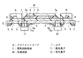
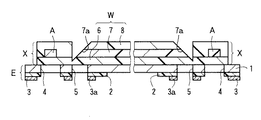
【解決手段】電気回路基板Eの表面に光導波路Wのコア7を形成する際に、コア7形成領域とアライメントマークA形成領域とをもつ感光性樹脂層から、1回のフォトリソグラフィ法により、コア7と同時に、光学素子位置決め用のアライメントマークAを形成する。そして、光学素子実装工程において、上記アライメントマークAを基準として、光導波路Wのコア7に対して適正な位置に、発光素子11および受光素子12を実装する。
【選択図】図1
Description
(1)ステンレス製基板1の裏面に電気回路3を形成して電気回路基板Eを作製する工程〔図2(a)〜(c)参照〕。
(2)上記電気回路基板Eのステンレス製基板1の表面に光導波路Wを作製する工程〔図3(a)〜(d)参照〕。
(3)上記光導波路Wのコア7の両端部を光反射部7aに形成する工程(図4参照)。
(4)上記電気回路3に発光素子11および受光素子12を実装する工程(図1参照)。
ステンレス製基板(厚み20μmのSUS304箔)の片面に、まず、フォトリソグラフィ法により、感光性ポリイミド樹脂からなる絶縁層(厚み10μm)を所定パターンに形成した。ついで、上記絶縁層の表面にスパッタリングにより、銅/ニッケル/クロム合金からなるシード層を形成した。つぎに、上記ステンレス製基板,絶縁層およびシード層からなる積層体の両面に、ドライフィルムレジストを貼着した後、上記シード層が形成されている側の上記ドライフィルムレジストに、フォトリソグラフィ法により、実装用パッドを含む電気回路のパターンの溝部を形成し、その溝部の底に上記シード層の表面部分を露呈させた。つぎに、電解銅めっきにより、上記溝部の底に露呈した上記シード層の表面部分に、電解銅めっき層(厚み20μm)を積層形成した。そして、上記ドライフィルムレジストを水酸化ナトリウム水溶液により剥離した。その後、上記電解銅めっき層が形成されていないシード層部分をソフトエッチングにより除去し、残存した電解銅めっき層とその下のシード層とからなる積層部分を電気回路に形成した。さらに、上記ステンレス製基板,絶縁層および電気回路からなる積層体の両面に、ドライフィルムレジストを貼着した後、片面側の上記ドライフィルムレジストに、フォトリソグラフィ法によりアライメントマーク視認用の貫通孔および光通過用の貫通孔のパターンの孔部を形成し、その孔部の底に上記ステンレス製基板の表面部分を露呈させた。つぎに、塩化第2鉄水溶液を用いたエッチングにより、上記孔部の底に露呈した上記ステンレス製基板部分を穿孔し、上記アライメントマーク視認用の貫通孔および光通過用の貫通孔をそれぞれ2個形成した。その後、上記実装用パッドの表面に、金/ニッケル合金めっき層を形成した。
下記の一般式(1)で示されるビスフェノキシエタノールフルオレングリシジルエーテル(成分A)35重量部、脂環式エポキシである3,4−エポキシシクロヘキセニルメチル−3’,4’−エポキシヘキセンカルボキシレート(ダイセル化学社製、セロキサイド2021P)(成分B)40重量部、シクロヘキセンオキシド骨格を有する脂環式エポキシ樹脂(ダイセル化学社製、セロキサイド2081)(成分C)25重量部、4,4’−ビス〔ジ(βヒドロキシエトキシ)フェニルスルフィニオ〕フェニルスルフィド−ビス−ヘキサフルオロアンチモネートの50%プロピオンカーボネート溶液(成分D)2重量部とを混合することにより、アンダークラッド層およびオーバークラッド層の形成材料を調製した。

上記成分A:70重量部、1,3,3−トリス{4−〔2−(3−オキセタニル)〕ブトキシフェニル}ブタン:30重量部、上記成分D:1重量部を乳酸エチルに溶解することにより、コアの形成材料を調製した。
上記ステンレス製基板のもう一方の片面(上記電気回路が形成された面とは反対側の面)に、上記アンダークラッド層の形成材料を塗布し、塗布層を形成した。その後、その塗布層の全面に、超高圧水銀灯を用いて積算光量1000mJ/cm2 (i線基準)の露光を行い、上記塗布層を硬化させた。つづいて、120℃×15分間のベーキング(加熱処理)を行うことにより、発生した酸を拡散させ、反応を完了させた。このようにしてアンダークラッド層(厚み10μm)を形成した。
上記光通過用の貫通孔に対応する光導波路の両端部を、エキシマレーザ(光源KrF:波長248nm)によるレーザ加工により、上記ステンレス製基板に対して45°傾斜した傾斜面に形成した。その後、エタノール中で超音波洗浄を行った。上記傾斜面のコア部分が光反射部である。
上記光反射部まで形成された生産中間物を、電気回路側の面を上に向けて実装機のステージ上にセットした。そして、その実装機に備えられている画像認識装置により、上記ステンレス製基板に形成されたアライメントマーク視認用の貫通孔を通して上記アライメントマークを視認した状態で、そのアライメントマークを基準として算出される上記コアの光反射部の位置に、発光素子および受光素子の光軸が合わさるよう、上記発光素子および受光素子を、上記光通過用の貫通孔の下方を覆うように実装した。このようにして、光電気混載基板を製造することができた。
E 電気回路基板
W 光導波路
7 コア
11 発光素子
12 受光素子
Claims (4)
- 電気回路基板を準備する工程と、この電気回路基板の回路形成面と反対側の面に光導波路形成用の感光性樹脂層を形成する工程と、上記感光性樹脂層のコア形成領域をフォトリソグラフィ法により所定パターンのコアに形成する工程をもつ光導波路作製工程と、上記光導波路の端部側に対応する上記電気回路基板の回路形成面の部分に光学素子を実装する工程と、上記光導波路の上記端部側に位置するコアの端部を,光を反射して上記コアと上記光学素子との間の光伝播を可能とする反射部に形成する工程と、上記電気回路基板に上記コアと上記光学素子との間の光伝播用の通路を設ける工程とを備え、上記感光性樹脂層としてコア形成領域とともにアライメントマーク形成領域をもつ感光性樹脂層を使用し、上記コアの形成と同時に、上記アライメントマーク形成領域を上記フォトリソグラフィ法により所定パターンのアライメントマークに形成する工程と、上記光学素子の実装を、上記アライメントマークを基準として所定の位置に行う工程とを有することを特徴とする光電気混載基板の製造方法。
- 上記光学素子の実装が、上記電気回路基板に形成されたアライメントマーク視認用の貫通孔から透視できる上記アライメントマークを目印にして行われる請求項1記載の光電気混載基板の製造方法。
- 上記光学素子が、上記コアの端部に対して光を出射する発光素子であり、上記反射部が上記発光素子からの出射光を反射する請求項1または2記載の光電気混載基板の製造方法。
- 上記光学素子が、上記コアの端部からの光を受光する受光素子であり、上記反射部が上記コア内からの光を反射する請求項1または2記載の光電気混載基板の製造方法。
Priority Applications (6)
| Application Number | Priority Date | Filing Date | Title |
|---|---|---|---|
| JP2008114329A JP5055193B2 (ja) | 2008-04-24 | 2008-04-24 | 光電気混載基板の製造方法 |
| KR1020090035369A KR101560404B1 (ko) | 2008-04-24 | 2009-04-23 | 광전기 혼재 기판의 제조 방법 |
| US12/428,669 US8142672B2 (en) | 2008-04-24 | 2009-04-23 | Manufacturing method of opto-electric hybrid board |
| AT09158611T ATE523803T1 (de) | 2008-04-24 | 2009-04-23 | Herstellungsverfahren für eine optoelektrische hybridplatte |
| EP09158611A EP2112534B1 (en) | 2008-04-24 | 2009-04-23 | Manufacturing method of opto-electric hybrid board |
| CN200910135371XA CN101566706B (zh) | 2008-04-24 | 2009-04-24 | 光电混合基板的制造方法 |
Applications Claiming Priority (1)
| Application Number | Priority Date | Filing Date | Title |
|---|---|---|---|
| JP2008114329A JP5055193B2 (ja) | 2008-04-24 | 2008-04-24 | 光電気混載基板の製造方法 |
Publications (2)
| Publication Number | Publication Date |
|---|---|
| JP2009265342A true JP2009265342A (ja) | 2009-11-12 |
| JP5055193B2 JP5055193B2 (ja) | 2012-10-24 |
Family
ID=40901955
Family Applications (1)
| Application Number | Title | Priority Date | Filing Date |
|---|---|---|---|
| JP2008114329A Expired - Fee Related JP5055193B2 (ja) | 2008-04-24 | 2008-04-24 | 光電気混載基板の製造方法 |
Country Status (6)
| Country | Link |
|---|---|
| US (1) | US8142672B2 (ja) |
| EP (1) | EP2112534B1 (ja) |
| JP (1) | JP5055193B2 (ja) |
| KR (1) | KR101560404B1 (ja) |
| CN (1) | CN101566706B (ja) |
| AT (1) | ATE523803T1 (ja) |
Cited By (15)
| Publication number | Priority date | Publication date | Assignee | Title |
|---|---|---|---|---|
| JP2012133171A (ja) * | 2010-12-22 | 2012-07-12 | Nitto Denko Corp | 光導波路の製法 |
| JP2012155215A (ja) * | 2011-01-27 | 2012-08-16 | Nitto Denko Corp | 光導波路の製法およびそれに用いられる光導波路体 |
| JP2012194287A (ja) * | 2011-03-15 | 2012-10-11 | Sumitomo Bakelite Co Ltd | 光電気混載基板の製造方法、光電気混載基板および電子機器 |
| EP2639612A1 (en) | 2012-03-16 | 2013-09-18 | Nitto Denko Corporation | Opto-electric hybrid board and method of manufacturing same |
| EP2639610A1 (en) | 2012-03-16 | 2013-09-18 | Nitto Denko Corporation | Opto-electric hybrid board and method of manufacturing same |
| EP2662716A1 (en) | 2012-05-08 | 2013-11-13 | Nitto Denko Corporation | Opto-electric hybrid board and method of manufacturing same |
| EP2685794A1 (en) * | 2012-07-13 | 2014-01-15 | Nitto Denko Corporation | Opto-electric hybrid board |
| EP2736309A1 (en) | 2012-11-27 | 2014-05-28 | Nitto Denko Corporation | Opto-electric hybrid board and method of manufacturing same |
| JP2014182208A (ja) * | 2013-03-18 | 2014-09-29 | Fujitsu Ltd | 光伝送装置の製造方法及び製造装置、並びに光伝送装置 |
| WO2014196252A1 (ja) * | 2013-06-06 | 2014-12-11 | 日東電工株式会社 | 光電気混載基板 |
| JP2015087475A (ja) * | 2013-10-29 | 2015-05-07 | 日東電工株式会社 | 光電気混載基板およびその製法 |
| KR20170076655A (ko) | 2014-10-24 | 2017-07-04 | 닛토덴코 가부시키가이샤 | 광전기 혼재 기판 및 그 제법 |
| KR20170076685A (ko) | 2014-10-28 | 2017-07-04 | 닛토덴코 가부시키가이샤 | 광전기 혼재 기판 |
| KR20170087871A (ko) | 2014-11-25 | 2017-07-31 | 닛토덴코 가부시키가이샤 | 광전기 혼재 기판 및 그 제법 |
| JPWO2021161915A1 (ja) * | 2020-02-12 | 2021-08-19 |
Families Citing this family (27)
| Publication number | Priority date | Publication date | Assignee | Title |
|---|---|---|---|---|
| JP5049145B2 (ja) * | 2008-01-22 | 2012-10-17 | 日東電工株式会社 | 光導波路デバイスの製法 |
| JP5138459B2 (ja) * | 2008-05-15 | 2013-02-06 | 新光電気工業株式会社 | 配線基板の製造方法 |
| JP5106348B2 (ja) | 2008-10-28 | 2012-12-26 | 日東電工株式会社 | 光電気混載モジュールの製造方法およびそれによって得られた光電気混載モジュール |
| JP4796615B2 (ja) * | 2008-11-26 | 2011-10-19 | 日東電工株式会社 | 光電気混載基板およびその製造方法 |
| JP2012208306A (ja) * | 2011-03-29 | 2012-10-25 | Nitto Denko Corp | 光電気混載基板およびその製法 |
| US9182544B2 (en) | 2011-12-21 | 2015-11-10 | Intel Corporation | Fabrication of planar light-wave circuits (PLCS) for optical I/O |
| US9377594B2 (en) | 2011-12-29 | 2016-06-28 | Intel Corporation | Two-dimensional, high-density optical connector |
| US9507086B2 (en) | 2011-12-30 | 2016-11-29 | Intel Corporation | Optical I/O system using planar light-wave integrated circuit |
| JP5877749B2 (ja) * | 2012-03-29 | 2016-03-08 | 日東電工株式会社 | 光電気混載基板の製法 |
| CN103389546B (zh) * | 2012-05-08 | 2016-12-07 | 鸿富锦精密工业(深圳)有限公司 | 光纤模组 |
| JP6081086B2 (ja) * | 2012-06-14 | 2017-02-15 | Tdk株式会社 | 光電素子用実装装置及び実装方法 |
| AT513747B1 (de) | 2013-02-28 | 2014-07-15 | Mikroelektronik Ges Mit Beschränkter Haftung Ab | Bestückungsverfahren für Schaltungsträger und Schaltungsträger |
| CN104101958B (zh) * | 2013-04-03 | 2017-10-03 | 赛恩倍吉科技顾问(深圳)有限公司 | 光通讯装置 |
| JP2014216377A (ja) * | 2013-04-23 | 2014-11-17 | イビデン株式会社 | 電子部品とその製造方法及び多層プリント配線板の製造方法 |
| TWI572933B (zh) * | 2013-05-20 | 2017-03-01 | 鴻海精密工業股份有限公司 | 光通訊裝置 |
| CN106537615B (zh) | 2014-08-04 | 2019-08-20 | 株式会社富士 | 安装装置 |
| JP6525240B2 (ja) * | 2014-10-24 | 2019-06-05 | 日東電工株式会社 | 光電気混載基板およびその製法 |
| CN104698552B (zh) * | 2015-03-16 | 2016-05-11 | 中国航天科技集团公司第九研究院第七七一研究所 | 一种用于航天器和军用计算机上的光互连基板及其制造方法 |
| DE102015207709A1 (de) * | 2015-04-27 | 2016-10-27 | Automotive Lighting Reutlingen Gmbh | Verfahren und Vorrichtung zur Anordnung eines Schaltungsträgers mit einer Halbleiterlichtquelle in einer bestimmten Lage relativ zu einem optischen System einer Beleuchtungseinrichtung |
| JP6649076B2 (ja) * | 2015-10-26 | 2020-02-19 | 京セラ株式会社 | 光回路基板の製造方法 |
| US9739942B2 (en) * | 2015-10-26 | 2017-08-22 | Kyocera Corporation | Method for manufacturing optical circuit board |
| JP7002886B2 (ja) * | 2017-08-22 | 2022-01-20 | 日東電工株式会社 | 光導波路、光電気混載基板、および光電気混載モジュール |
| JP6677232B2 (ja) * | 2017-09-29 | 2020-04-08 | 日亜化学工業株式会社 | 発光装置の製造方法 |
| JP7489756B2 (ja) | 2018-07-25 | 2024-05-24 | 日東電工株式会社 | 光学素子装置およびその製造方法 |
| US10775573B1 (en) * | 2019-04-03 | 2020-09-15 | International Business Machines Corporation | Embedding mirror with metal particle coating |
| US12366715B2 (en) * | 2020-07-29 | 2025-07-22 | Nitto Denko Corporation | Opto-electric hybrid board |
| CN115407450B (zh) * | 2021-05-28 | 2025-09-02 | 华为技术有限公司 | 光波导和光束辅助对准的方法 |
Citations (4)
| Publication number | Priority date | Publication date | Assignee | Title |
|---|---|---|---|---|
| JP2000298217A (ja) * | 1999-04-13 | 2000-10-24 | Toppan Printing Co Ltd | 光・電気配線基板及び製造方法並びに実装基板 |
| JP2004361858A (ja) * | 2003-06-06 | 2004-12-24 | Sharp Corp | マイクロレンズ付き光導波路およびその製造方法 |
| JP2006030798A (ja) * | 2004-07-20 | 2006-02-02 | Shinko Electric Ind Co Ltd | 光モジュールの製造方法および光伝搬部材の製造方法 |
| JP2006140233A (ja) * | 2004-11-10 | 2006-06-01 | Ibiden Co Ltd | 光電気配線板、および、光通信用デバイス |
Family Cites Families (5)
| Publication number | Priority date | Publication date | Assignee | Title |
|---|---|---|---|---|
| JP2000199827A (ja) | 1998-10-27 | 2000-07-18 | Sony Corp | 光導波装置およびその製造方法 |
| TW451084B (en) | 1999-06-25 | 2001-08-21 | Toppan Printing Co Ltd | Optical-electro wiring board, mounted board, and manufacturing method of optical-electro wiring board |
| EP1122561A1 (en) * | 2000-02-03 | 2001-08-08 | Corning Incorporated | High precision alignment of optical devices over a high thickness transparent layer |
| JP2006120956A (ja) | 2004-10-22 | 2006-05-11 | Ibiden Co Ltd | 多層プリント配線板 |
| JP2007173375A (ja) | 2005-12-20 | 2007-07-05 | Nec Corp | 複合実装デバイス及びその製造方法 |
-
2008
- 2008-04-24 JP JP2008114329A patent/JP5055193B2/ja not_active Expired - Fee Related
-
2009
- 2009-04-23 AT AT09158611T patent/ATE523803T1/de not_active IP Right Cessation
- 2009-04-23 KR KR1020090035369A patent/KR101560404B1/ko not_active Expired - Fee Related
- 2009-04-23 US US12/428,669 patent/US8142672B2/en not_active Expired - Fee Related
- 2009-04-23 EP EP09158611A patent/EP2112534B1/en not_active Not-in-force
- 2009-04-24 CN CN200910135371XA patent/CN101566706B/zh not_active Expired - Fee Related
Patent Citations (4)
| Publication number | Priority date | Publication date | Assignee | Title |
|---|---|---|---|---|
| JP2000298217A (ja) * | 1999-04-13 | 2000-10-24 | Toppan Printing Co Ltd | 光・電気配線基板及び製造方法並びに実装基板 |
| JP2004361858A (ja) * | 2003-06-06 | 2004-12-24 | Sharp Corp | マイクロレンズ付き光導波路およびその製造方法 |
| JP2006030798A (ja) * | 2004-07-20 | 2006-02-02 | Shinko Electric Ind Co Ltd | 光モジュールの製造方法および光伝搬部材の製造方法 |
| JP2006140233A (ja) * | 2004-11-10 | 2006-06-01 | Ibiden Co Ltd | 光電気配線板、および、光通信用デバイス |
Cited By (37)
| Publication number | Priority date | Publication date | Assignee | Title |
|---|---|---|---|---|
| US9110237B2 (en) | 2010-12-22 | 2015-08-18 | Nitto Denko Corporation | Method of manufacturing optical waveguide |
| JP2012133171A (ja) * | 2010-12-22 | 2012-07-12 | Nitto Denko Corp | 光導波路の製法 |
| JP2012155215A (ja) * | 2011-01-27 | 2012-08-16 | Nitto Denko Corp | 光導波路の製法およびそれに用いられる光導波路体 |
| JP2012194287A (ja) * | 2011-03-15 | 2012-10-11 | Sumitomo Bakelite Co Ltd | 光電気混載基板の製造方法、光電気混載基板および電子機器 |
| US8768114B2 (en) | 2012-03-16 | 2014-07-01 | Nitto Denko Corporation | Opto-electric hybrid board and method of manufacturing same |
| EP2639612A1 (en) | 2012-03-16 | 2013-09-18 | Nitto Denko Corporation | Opto-electric hybrid board and method of manufacturing same |
| EP2639610A1 (en) | 2012-03-16 | 2013-09-18 | Nitto Denko Corporation | Opto-electric hybrid board and method of manufacturing same |
| KR20130105360A (ko) | 2012-03-16 | 2013-09-25 | 닛토덴코 가부시키가이샤 | 광전기 혼재 기판 및 그 제조 방법 |
| KR20130105359A (ko) | 2012-03-16 | 2013-09-25 | 닛토덴코 가부시키가이샤 | 광전기 혼재 기판 및 그 제조 방법 |
| US9046646B2 (en) | 2012-03-16 | 2015-06-02 | Nitto Denko Corporation | Opto-electric hybrid board and method of manufacturing same |
| US8837874B2 (en) | 2012-05-08 | 2014-09-16 | Nitto Denko Corporation | Opto-electric hybrid board and method of manufacturing same |
| EP2662716A1 (en) | 2012-05-08 | 2013-11-13 | Nitto Denko Corporation | Opto-electric hybrid board and method of manufacturing same |
| JP2014021203A (ja) * | 2012-07-13 | 2014-02-03 | Nitto Denko Corp | 光電気混載基板 |
| KR20140009022A (ko) | 2012-07-13 | 2014-01-22 | 닛토덴코 가부시키가이샤 | 광전기 혼재 기판 |
| US9366815B2 (en) | 2012-07-13 | 2016-06-14 | Nitto Denko Corporation | Opto-electric hybrid board |
| EP2685794A1 (en) * | 2012-07-13 | 2014-01-15 | Nitto Denko Corporation | Opto-electric hybrid board |
| EP2736309A1 (en) | 2012-11-27 | 2014-05-28 | Nitto Denko Corporation | Opto-electric hybrid board and method of manufacturing same |
| KR20140068756A (ko) | 2012-11-27 | 2014-06-09 | 닛토덴코 가부시키가이샤 | 광 전기 혼재 기판 및 그 제조 방법 |
| JP2014106355A (ja) * | 2012-11-27 | 2014-06-09 | Nitto Denko Corp | 光電気混載基板およびその製法 |
| US9297958B2 (en) | 2012-11-27 | 2016-03-29 | Nitto Denko Corporation | Opto-electric hybrid board and method of manufacturing same |
| JP2014182208A (ja) * | 2013-03-18 | 2014-09-29 | Fujitsu Ltd | 光伝送装置の製造方法及び製造装置、並びに光伝送装置 |
| JP2014238455A (ja) * | 2013-06-06 | 2014-12-18 | 日東電工株式会社 | 光電気混載基板 |
| KR102189206B1 (ko) | 2013-06-06 | 2020-12-09 | 닛토덴코 가부시키가이샤 | 광전기 혼재 기판 |
| KR20160019058A (ko) * | 2013-06-06 | 2016-02-18 | 닛토덴코 가부시키가이샤 | 광전기 혼재 기판 |
| WO2014196252A1 (ja) * | 2013-06-06 | 2014-12-11 | 日東電工株式会社 | 光電気混載基板 |
| US9632246B2 (en) | 2013-06-06 | 2017-04-25 | Nitto Denko Corporation | Opto-electric hybrid board |
| JP2015087475A (ja) * | 2013-10-29 | 2015-05-07 | 日東電工株式会社 | 光電気混載基板およびその製法 |
| US9618710B2 (en) | 2013-10-29 | 2017-04-11 | Nitto Denko Corporation | Opto-electric hybrid board and production method therefor |
| WO2015064355A1 (ja) * | 2013-10-29 | 2015-05-07 | 日東電工株式会社 | 光電気混載基板およびその製法 |
| KR20170076655A (ko) | 2014-10-24 | 2017-07-04 | 닛토덴코 가부시키가이샤 | 광전기 혼재 기판 및 그 제법 |
| US10353161B2 (en) | 2014-10-24 | 2019-07-16 | Nitto Denko Corporation | Opto-electric hybrid board and method of manufacturing same |
| US9989720B2 (en) | 2014-10-28 | 2018-06-05 | Nitto Denko Corporation | Opto-electric hybrid board |
| KR20170076685A (ko) | 2014-10-28 | 2017-07-04 | 닛토덴코 가부시키가이샤 | 광전기 혼재 기판 |
| KR20170087871A (ko) | 2014-11-25 | 2017-07-31 | 닛토덴코 가부시키가이샤 | 광전기 혼재 기판 및 그 제법 |
| US10295769B2 (en) | 2014-11-25 | 2019-05-21 | Nitto Denko Corporation | Opto-electric hybrid board and method of manufacturing same |
| JPWO2021161915A1 (ja) * | 2020-02-12 | 2021-08-19 | ||
| WO2021161915A1 (ja) * | 2020-02-12 | 2021-08-19 | 日東電工株式会社 | 光電気混載基板および光電気複合伝送モジュール |
Also Published As
| Publication number | Publication date |
|---|---|
| CN101566706B (zh) | 2012-10-10 |
| JP5055193B2 (ja) | 2012-10-24 |
| KR101560404B1 (ko) | 2015-10-14 |
| US20090269704A1 (en) | 2009-10-29 |
| EP2112534A1 (en) | 2009-10-28 |
| KR20090112585A (ko) | 2009-10-28 |
| EP2112534B1 (en) | 2011-09-07 |
| CN101566706A (zh) | 2009-10-28 |
| ATE523803T1 (de) | 2011-09-15 |
| US8142672B2 (en) | 2012-03-27 |
Similar Documents
| Publication | Publication Date | Title |
|---|---|---|
| JP5055193B2 (ja) | 光電気混載基板の製造方法 | |
| JP4971248B2 (ja) | 光電気混載モジュールの製造方法 | |
| JP4754613B2 (ja) | 光電気混載基板およびその製造方法 | |
| JP5877749B2 (ja) | 光電気混載基板の製法 | |
| JP4796615B2 (ja) | 光電気混載基板およびその製造方法 | |
| JP5160941B2 (ja) | 光導波路モジュールの製造方法 | |
| JP5106348B2 (ja) | 光電気混載モジュールの製造方法およびそれによって得られた光電気混載モジュール | |
| JP5271141B2 (ja) | 光電気混載モジュールの製造方法およびそれによって得られた光電気混載モジュール | |
| JP5608125B2 (ja) | 光電気混載基板およびその製法 | |
| CN107003476B (zh) | 光电混合基板 | |
| JP2015087475A (ja) | 光電気混載基板およびその製法 | |
| JP5608122B2 (ja) | 光電気混載基板およびその製法 | |
| JP2005134577A (ja) | 自己形成光導波路構造体、光電気複合配線構造体 | |
| JP2005134576A (ja) | 自己形成光導波路構造体、光電気複合配線構造体 |
Legal Events
| Date | Code | Title | Description |
|---|---|---|---|
| A621 | Written request for application examination |
Free format text: JAPANESE INTERMEDIATE CODE: A621 Effective date: 20101122 |
|
| A131 | Notification of reasons for refusal |
Free format text: JAPANESE INTERMEDIATE CODE: A131 Effective date: 20120131 |
|
| A977 | Report on retrieval |
Free format text: JAPANESE INTERMEDIATE CODE: A971007 Effective date: 20120201 |
|
| A521 | Request for written amendment filed |
Free format text: JAPANESE INTERMEDIATE CODE: A821 Effective date: 20120315 Free format text: JAPANESE INTERMEDIATE CODE: A523 Effective date: 20120315 |
|
| TRDD | Decision of grant or rejection written | ||
| A01 | Written decision to grant a patent or to grant a registration (utility model) |
Free format text: JAPANESE INTERMEDIATE CODE: A01 Effective date: 20120724 |
|
| A01 | Written decision to grant a patent or to grant a registration (utility model) |
Free format text: JAPANESE INTERMEDIATE CODE: A01 |
|
| A61 | First payment of annual fees (during grant procedure) |
Free format text: JAPANESE INTERMEDIATE CODE: A61 Effective date: 20120730 |
|
| R150 | Certificate of patent or registration of utility model |
Ref document number: 5055193 Country of ref document: JP Free format text: JAPANESE INTERMEDIATE CODE: R150 Free format text: JAPANESE INTERMEDIATE CODE: R150 |
|
| FPAY | Renewal fee payment (event date is renewal date of database) |
Free format text: PAYMENT UNTIL: 20150803 Year of fee payment: 3 |
|
| R250 | Receipt of annual fees |
Free format text: JAPANESE INTERMEDIATE CODE: R250 |
|
| R250 | Receipt of annual fees |
Free format text: JAPANESE INTERMEDIATE CODE: R250 |
|
| R250 | Receipt of annual fees |
Free format text: JAPANESE INTERMEDIATE CODE: R250 |
|
| R250 | Receipt of annual fees |
Free format text: JAPANESE INTERMEDIATE CODE: R250 |
|
| R250 | Receipt of annual fees |
Free format text: JAPANESE INTERMEDIATE CODE: R250 |
|
| R250 | Receipt of annual fees |
Free format text: JAPANESE INTERMEDIATE CODE: R250 |
|
| R250 | Receipt of annual fees |
Free format text: JAPANESE INTERMEDIATE CODE: R250 |
|
| R250 | Receipt of annual fees |
Free format text: JAPANESE INTERMEDIATE CODE: R250 |
|
| LAPS | Cancellation because of no payment of annual fees |